
Abstract
The bonding forces and atomic sizes determine the arrangement of the atoms in equilibrium in crystals. The crystal structure is determined by the tendency to fill a given space with the maximum number of atoms under the constraint of bonding forces and atomic radii. Crystal bonding and crystal structure are thus intimately related to each other and determine the intrinsic properties of semiconductors. Nonequilibrium states can be frozen-in and determine the structure of amorphous semiconductors. In an amorphous structure the short-range order is much like that in a crystal, while long-range periodicity does not exist. Quasicrystals are solids with an order between crystalline and amorphous. These quasiperiodic crystals have no three-dimensional translational periodicity, but exhibit long-range order in a diffraction experiment. A quasicrystalline pattern continuously fills all available space; unlike regular crystals space filling requires an aperiodic repetition of (at least) two different unit cells.
Superlattices and low-dimensional structures like quantum wires and quantum dots, created by alternating thin depositions of different semiconductors, show material properties which can be engineered by designing size and chemical composition. This opens the feasibility for fabricating new and improved devices.
Access provided by CONRICYT-eBooks. Download reference work entry PDF
Keywords
- Bonding forces
- Bravais lattice
- Brillouin zone
- Crystal structure
- Atomic radii
- Crystal bonding
- Miller indices
- Organic semiconductors
- Structure of amorphous semiconductors
- Short-range order
- Quasicrystals
- Superlattices
- Quantum wells
- Quantum wires
- Quantum dots
- Reciprocal lattice
- Unit cell
1 Structure and Symmetry in Crystalline Solids
Many physical properties of crystals depend on the periodicity and symmetry of the lattice that determines its crystal structure . A short summary of the basic elements of the crystal structure is presented in this chapter. For an extensive review, see DiBenedetto (1967), Newnham (1975), and Barrett and Massalski (1980).
The easiest way to define the structure of a crystalline semiconductor (Fig. 1) is by its smallest three-dimensional building block, the unit cell . From these unit cells, the ideal crystal is constructed by three-dimensional repetition. The unit cell usually contains a small number of atoms, from one for a primitive unit cell to a few atoms for nonprimitive cells and compound crystals. In molecular crystals, this number can be much larger and is usually a small multiple of the number of molecules forming the crystal. The three-dimensional periodic array of atoms is called the crystal lattice.

Diamond structure viewed along a 〈110〉 direction (Goncharova 2012)
To define a unit cell, one introduces a three-dimensional point lattice and adds to this imaginary lattice an atomic basis , i.e., one, two, or more atoms in a specific arrangement for each point, in order to arrive at the crystal lattice (Klug and Alexander 1974; Buerger 1956). Figure 2 shows in two dimensions a crystal with a basis containing two atoms.

The crystal lattice: point lattice plus basis with two atoms
1.1 Crystal Systems and Bravais Lattices
A coordinate system is introduced so that its origin lies at the center of an arbitrary atom (or basis) and its axes point through the centers of preferably adjacent atoms (or basis) while best representing the symmetry of the latticeFootnote 1 – see Fig. 5. A lattice vector points from the origin along each axis to the center of the next equivalent atomFootnote 2 or from the center of one basis to the center of the next. The value of this vector is called the lattice constant .
1.1.1 Crystal Systems
All possible crystals can be ordered into seven crystal systems (i.e., different coordinate systems) according to the relative length of their lattice vectors and the angle between these vectors – see Fig. 3. These crystal systems are listed in Table 1, together with other properties identified in the following sections.

Coordinate system and angles between lattice vectors within a crystal
1.1.2 Bravais Lattices
There are several symmetry operations that transfer a crystal into itself. The simplest one is a linear transformation, which transfers the lattice point t 0 into an equivalent lattice point t:
with a, b, and c as the lattice vectors in x-, y-, and z-directions, respectively, and integers n l, n 2, and n 3. This linear transformation shifts the entire lattice by an integer number of lattice constants and thereby reproduces the lattice. All lattices show linear transformation symmetry. A unit cell can now be defined as the smallest parallelepiped that forms the entire crystal when sequentially shifted by a linear transformation according (1). There are only 14 different unit cells possible; they form 14 different lattices, called Bravais lattices (or translation lattices).
In each of the crystal systems, there is one lattice with a unit cell that contains only one lattice atom,Footnote 3 the primitive unit cell (P in Table 1). In some crystal systems, there exist lattices with unit cells containing more than one atom per cell. For example, in the orthorhombic system the extra atom(s) may sit in the center of the unit cell (body centered, I), in the center of the base [(a + b)/2, base centered, C], or in the center of all facesFootnote 4 (face centered, F), as shown in Fig. 4. All Bravais lattices are listed in the last column of Table 1.

Unit cells of the orthorhombic Bravais lattice. (a) Primitive P, (b) body-centered I, (c) base-centered C, and (d) face-centered F. Upper row: fractional atoms shown within each unit cell, lower row: number of atoms per unit cell indicated
1.1.3 The Primitive Unit Cell
Occasionally one needs to describe the lattice as subdivided into primitive cells, while filling the entire space without voids. This can always be done; an example is presented in Fig. 5. The figure shows a face-centered cubic lattice with four lattice atoms in its unit cell. If the orthogonal system of crystal axes is replaced with one connecting the corner atom to the nearest face-centered atom, the crystal structure becomes trigonal with

Face-centered cubic unit cell with inscribed trigonal primitive cell (blue lines)
The cubic system is usually preferred because of a simpler mathematical description, but the trigonal representation is totally equivalent to it. This example shows that for a given crystal, the choice of a certain crystal system is not unique.
1.2 Point Groups (Crystal Classes) and Space Groups
1.2.1 Point Groups
The other symmetry operations, excluding any translation, are rotation, reflection (composed from rotation and inversion on a plane), and inversion, i.e., “reflection” at a point. Crystals that are distinguished by one or a combination of these can be divided into 32 different crystal classes. These symmetry operations are applied to the basis about a point of the Bravais lattice and therefore are also called point groups. The symmetry operations are usually identified by their Schönflies or Hermann–Mauguin symbol.
The Schönflies symbol identifies with capital letters C, D, T, and O the basic symmetry: cyclic, dihedral, tetrahedral, and octahedral. A subscript is used to identify the rotational symmetry, e.g., D3 has threefold symmetry. Another index, v, h, d is used for further distinction – see, e.g., Brown and Forsyth (1973).
The Hermann–Mauguin nomenclature indicates the type of symmetry directly from the symbol. It is a combination of numbers (n) and the letter m: n indicates rotational symmetry (for n = 2, 3, 4, or 6, an n-fold symmetry) and \( \overline{n} \) denotes either an inversion (\( \overline{\mathrm{l}} \)) or a roto-inversion (with a \( \overline{3} \)-, \( \overline{4} \)-, or \( \overline{6} \)-fold symmetry); m indicates a mirror plane parallel to, and \( \frac{n}{m} \) perpendicular to, the rotational axis with n-fold symmetry. Repetition of m or other symbols indicates the symmetry about the other orthogonal planes or axes – see, e.g., Hahn (1983).
All possible combinations of rotation, reflection, and inversion are listed in Table 1, with both symbols to identify each of the 32 point groups.
1.2.2 Space Groups
Combining the symmetry operations leading to the point groups with nonprimitive translation yields a total of 230 space groups. Alternatively, there are 1421 space groups when the ordering of spins is also considered (Birss 1964). They include screw axis and glide plane operations; the former combines translation (shifting) with rotation; the latter combines translation with reflection.
The Schönflies symbol for space groups designates the different possibilities of combining the symmetry operations by a superscript referring to the point group symbol (e.g., O 7h for Si).
In the Hermann–Mauguin symbol, the Bravais lattice identifier is added: A, B, and C (identifying the specific base for face-centered symmetry)Footnote 5; P (primitive); I, F, and R (rhombohedric); and H (hexagonal). In addition, small letters, a, b, c, d, or n, are appended to identify specific glide planes – namely, at a/2, b/2, and c/2, \( \frac{r+s}{4} \), and \( \frac{r+s}{2} \), for a, b, c, d, and n, respectively, with r and s standing for any a, b, or c. Footnote 6
Typical element semiconductors have Oh symmetry, e.g., diamond O 7h (or Fd3m) for Ge and Si. Other binary semiconductors have zincblende T 2d (or F43m) for GaAs, wurtzite C 46v (P63 mc) for GaN, or rock salt O 5h (or Fm3m) for NaCl.
In summary, crystals are classified according to their lattice symmetry in four different ways, depending on the type of symmetry operation employed. This is shown in Table 2.
1.2.3 Crystallographic Notations
A lattice point is identified by the coefficients of the lattice vector pointing to it:
A lattice point is conventionally given by the three coefficients without brackets:
A lattice direction is identified by a line pointing in this direction. When this line is shifted parallel so that it passes through the origin, the position of the nearest lattice point on this line, identified by the coefficients of Eq. 2 and enclosed in square brackets, defines this direction:
Conveniently, one may reduce this notation by permitting simple fractions; for example, [221] may also be written as [1 1 1/2]. Negative coefficients are identified by a bar: [\( 00\overline{1} \)] = -[001] is a vector pointing downward.
Equivalent directions are directions which are crystallographically equivalent; for example, in a cube these are the directions [100], [010], [001], [\( \overline{1}00 \)], [\( 0\overline{1}0 \)] and [\( 00\overline{1} \)]. All of these are meant when one writes 〈100〉; in general
A lattice plane is described by Miller indices . These are obtained by taking the three coefficients of the intercepts of this plane with the three axes n 1, n 2, and n 3; forming the reciprocals of these coefficients 1/n 1 1/n 2 1/n 3; and clearing the fractions. For example, for a plane parallel to c and intersecting the x-axis at 2a (see Fig. 6) and the y-axis at 4b, the fractions are ½ ¼ \( \frac{1}{\infty } \). Thus, the Miller indices are (210) and are enclosed in parentheses. The general form is

Example of a (210) plane
A family of planes which are crystallographically equivalent [such as (111), (\( \overline{1}11 \)), (\( 1\overline{1}1 \)), (\( 11\overline{1} \)), (\( \overline{1} \overline{1} 1 \)), etc.] is identified by the Miller indices in curly parentheses. For this example the triple is {111}; in general, it is
The Miller indices notation is a reciprocal lattice representation (see Sect. 1.3). It is quite useful for the discussion of interference phenomena, which requires the knowledge of distances between equivalent planes. The distance between the {hkl} planes is easily found; in a cubic system, it is simply
with a the lattice constant. In other crystal systems the expressions are slightly more complicatedFootnote 7 (see Warren 1990; Zachariasen 2004; and James 1954 for more details).
The reciprocal lattice is a lattice in which each point relates to a corresponding point of the actual lattice by a reciprocity relation given below (Eqs. 6–10).
1.2.4 Morphology of Similar Crystals
When a specific chemical compound crystallizes in different crystal classes, it is called a polymorph . When crystals with the same structure are formed by compounds in which only one element is exchanged with a homologous element, they are referred to as morphotrop . When similar compounds crystallize in a similar crystal form, they are called isomorph when they also have other physical properties in common, such as similar cation to anion radii ratio and similar polarizability.
1.3 The Reciprocal Lattice
As indicated above, the introduction of a reciprocal lattice is advantageous when one needs to identify the distance between equivalent lattice planes. This is of help for all kinds of interference phenomena, such as x-ray diffraction, the behavior of electrons when taken as waves, or lattice oscillations themselves. In a quantitative description, the relevant waves are described by wave functions of the typeFootnote 8
where A is the amplitude factor, r is a vector in real space, and k is a vector in reciprocal space. Here, k is referred to as the wave vector , or wave number, if only one relevant dimension is discussed; the wavevector is normal to the wave front and has the magnitude
with λ the wavelength. Since k · r is dimensionless, k has the dimension of reciprocal length. Multiplied by ħ, (=h/2π, where h is the Planck constant) ħ k has the physical meaning of a momentum as will be shown in Sect. 2.1 in chapter “The Origin of Band Structure.”
When R n is a lattice vector [for ease of mathematical description, we now change from (a, b, c) to (a 1, a 2, a 3)]
one obtains the corresponding vector K m in reciprocal space with the three fundamental vectors b l, b 2, and b 3:
where both sets of unit vectors are related by the orthogonal relation
where δ ij is the Kronecker delta symbol
The orthogonal relation can also be expressed by
that is, every vector in the reciprocal lattice is normal to the corresponding plane of the crystal lattice and its length is equal to the reciprocal distance between two neighboring corresponding lattice planes (see Kittel 2007). This definition is distinguished by a factor 2π from the definition of a reciprocal lattice found by crystallographers. This factor is included here to make the units of the reciprocal space identical to the wavevector units.
1.3.1 Wigner–Seitz Cells and Brillouin Zones
As knowledge about an entire crystal can be derived from the periodic repetition of its smallest unit, the unit cell , one can derive knowledge about the wave behavior from an equivalent cell in the reciprocal lattice. A convenient way to introduce this discussion is by examining the Wigner–Seitz cell rather than the unit cell itself.
A Wigner–Seitz cell is formed when a lattice point is connected with all equivalent neighbors, and planes are erected normal to and in the center of each of these interconnecting lines. An example is shown in Fig. 7, where for the face-centered unit cell (a 1, a 2, a 3), the Wigner–Seitz cell is constructed; the plane orthogonal to and intersecting the lattice vector a 2 is visible.

Face-centered cubic lattice (blue atoms on the black cube) with primitive parallelepiped (red lines) and from it the derived Wigner–Seitz cell in real space (blue polyhedron), which is equivalent to the Brillouin zone in reciprocal space
When such a Wigner–Seitz cell is constructed from the unit cell of the reciprocal lattice, the resulting cell is called the first Brillouin zone . It is the basic unit for describing lattice oscillations and electronic phenomena.
Most semiconductors crystallize with cubic or hexagonal lattices; by contrast, organic semiconductors have low-symmetry – often monoclinic – unit cells. The first Brillouin zones of these lattices are given in Fig. 8 and will be referred to frequently later in the book.

Brillouin zones for the three cubic, hexagonal, and monoclinic lattices with important symmetry points and axes. (a) Primitive, (b) face-centered, and (c) body-centered cubic lattice, (d) primitive hexagonal, and (e) simple monoclinic lattice
In these discussions, lattice symmetry is of great importance, and points about which certain symmetry operations can reproduce the lattice are often cited. These symmetry points can also be transformed into the reciprocal lattice and are identified here by specific letters. The most important symmetry points with their conventional notations are identified in the different Brillouin zones of Fig. 8. Γ is always the center of the zone (k x = k y = k z = 0), and in any of the cubic lattices, X is the intersection of the Brillouin zone surface with any of the main axes (k x , k y , or k z ); the points Δ, Λ, and Σ in face-centered cubic lattices lie halfway between Γ and X, Γ and L, and Γ and K, as shown in Fig. 8b. The positions of the other symmetry points (H, K, L, etc.) can be obtained directly from Fig. 8. In the hexagonal and monoclinic lattices other letters are used by convention as shown in Fig. 8.
The extent of the first Brillouin zone can easily be identified. For instance, in a primitive orthorhombic lattice with its unit cell extending to a, b, and c in the x-, y-, and z-directions, respectively, the first Brillouin zone extends from \( -\frac{\pi }{a} \) to \( \frac{\pi }{a} \) in k x -, from \( -\frac{\pi }{b} \) to \( \frac{\pi }{b} \) in k y -, and from \( -\frac{\pi }{c} \) to \( \frac{\pi }{c} \) in k z -direction. Since the wave equation is periodic in r and k, all relevant information is contained within the first Brillouin zone.
1.4 Relevance of Symmetry to Semiconductors
Lattice periodicity is one of the major factors in determining the band structure of semiconductors – see chapter “The Origin of Band Structure.” The symmetry elements of the lattice are reflected in the corresponding symmetry elements of the bands, from which important qualitative information about the electronic structure of a semiconductor is obtained. Therefore, the main features of the symmetry of some of the typical semiconductors are summarized below. A comprehensive review of element and compound structures is given by Wells (2012).
1.4.1 Elemental Semiconductors and Binary Semiconducting Compounds
1.4.1.1 Elemental Semiconductors
Most of the important crystalline semiconductors are elements (Ge, Si) or binary compounds (III–V or II–VI). They form crystals in which each atom is surrounded by four nearest neighbors,Footnote 9 i.e., they have a coordination number of 4. The connecting four atoms (ligands) surround each atom in the equidistant corners of a tetrahedron. The lattice is formed so that each of the surrounding atoms is again the center atom of an adjacent tetrahedron, as shown for two such tetrahedra in Fig. 9. Of the two principal possibilities for arranging two tetrahedra, only one is realized in nature for elemental crystals: the diamond lattice , wherein the base triangles of the intertwined tetrahedra are rotated by 60°. Ge and Si are examples. In amorphous elemental semiconductors, however, both possibilities of arranging the tetrahedra are realized – see Sect. 3.1.

Side and top view of two intertwined tetrahedra with (a) base triangles parallel (dihedral angle 0°) and (b) base triangles rotated by 60°
1.4.1.2 Binary Semiconducting Compounds
Binary III–V and II–VI compounds are formed by both tetrahedral arrangements which are dependent on relative atomic radii and preferred valence angles (see Sect. 1 in chapter “Crystal Bonding”), although with alternating atoms as nearest neighbors. These compounds can be thought of as an element (IV) semiconductor after replacing alternating atoms with an atom of the adjacent rows of elements (III and V). Similarly, II–VI compounds can be created by using elements from the next-to-adjacent rows – see Fig. 10 and Fig. 3 in chapter “Properties and Growth of Semiconductors”.

Binary compounds with semiconducting properties
Aside from these classical AB compounds, there are others that have interesting semiconducting (specifically thermoelectrical) properties. Examples include the II–V compounds (such as ZnSb, ZnAs, CdSb, or CdAs), which have orthorhombic structures. For a review, see Arushanov (1986).
The diamond lattice for AB compounds results in a zincblende lattice shown in Fig. 11a. Most III–V compounds, as, for instance, GaAs, are examples.

(a) Zincblende lattice (GaAs) constructed from two interpenetrating face-centered cubic sublattices of Ga and As, with a displaced origin at a/4, a/4, a/4, with a the edge length of the elementary cube. (b) Wurtzite lattice (CdS, GaN) constructed from two intertwined hexagonal sublattices of Cd and S (or, Ga and N)
Unrotated interpenetrating tetrahedra, as shown in Fig. 9a, produce the wurtzite lattice (Fig. 11b) which can also be obtained for a number of AB compounds. Examples include ZnS, CdS, and GaN. The aforementioned semiconductors can also crystallize in a zincblende modification. Under certain conditions, alternating layers of wurtzite and zincblende, each several atomic layers thick, are observed. This is called a polytype . Often, the zincblende structure is more stable at lower temperatures and the wurtzite structure appears above a transition temperature (1053 °C in CdS). With rapid cooling the wurtzite structure can be frozen-in.
Other structures of binary semiconductors include:
-
NaCl-type semiconductors, with PbTe as an example
-
Cinnabar (deformed NaCl) structures, with HgS as an example
-
Antifluorite silicide structures, with Mg2Si as an example. These structures can be regarded as derived from the fcc lattice (Fig. 11a) with one of the two interstitial positions filled by the second metal atom, similar to the Nowotny–Juza compounds in Sect. 1.4.2 below, and
-
A 3 I B IV structures, with Cs3Si as an example. For a review, see Parthé (1964), Sommer (1968), and Abrikosov et al. (1969).
1.4.2 Ternary and Quaternary Semiconducting Compounds
There are several classes of ternary and quaternary compounds with known attractive semiconducting properties. All have tetrahedral structures: each atom is surrounded by four neighbors. Some examples are discussed in the following sections. For a review, see Zunger (1985).
One can conceptually form a wide variety of ternary, quaternary, or higher compounds which have desirable semiconducting properties by replacing within a tetrahedral lattice, subsequent to the original replacement shown in Fig. 10, certain atoms with those from adjacent rows, as given in Fig. 12. These examples represent a large number (~140) of such compounds and indicate the rules for this type of compound formation. For instance, a II–III2–VI4 compound can be formed by replacing 8 atoms of column IV first with 4 atoms each of columns II and VI and consequently the 4 atoms of column II with one vacancy (0), one atom of column II, and two atoms of column III.

Construction of pseudobinaries (b), ternaries (a, c, d, e) pseudoternaries (g, h), and quaternaries (f) from element (IV) semiconductors (0 represents a vacancy, i.e., a missing atom at a lattice position)
1.4.2.1 Ternary Chalcopyrites
Best researched are the ternary chalcopyrites I–III–VI2; they are constructed from two zincblende lattices in which the metal atoms are replaced by an atom from each of the adjacent columns. In a simple example one may think of the two Zn atoms from ZnS as transmuted into Cu and Ga:
with some deformation of the zincblende lattice, since the Cu–S and Ga–S bonds have different strengths, and with a unit cell twice the size of that in the ZnS lattice (Fig. 13). For a review, see Miller et al. (1981).

(a) ZnS (or GaP) double unit cell; (b) CuGaS2 (or ZnGeP2) unit cell
1.4.2.2 Ternary Pnictides and ABC2 Compounds
Other ternaries with good semiconducting properties are the ternary pnictides II–IV–V2 (such as ZnSiP2) which have the same chalcopyrite structure and, in a similar example, can be constructed from GaP by the transmutation
Still another class with chalcopyrite structure is composed of the I–III–VI2 compounds, of which CuFeS2 is representative. (These structures are reviewed by Jaffe and Zunger 1984).
1.4.2.3 Nowotny–Juza Compounds
Interesting variations of this tetrahedral structure (see Parthé 1972) are the Nowotny–Juza compounds, which are partially filled tetrahedral interstitial I–II–V compounds (e.g., LiZnN). Here the Li atom is inserted into exactly one half of the available interstitial sites of the zincblende lattice (e.g., on V a or on V c as shown in Fig. 14). A substantial preference for the Li atom to occur at the site closer to the N atom (rather than the site next to the Zn – the lattice energy of this structure is lower by about 1 eV) makes this compound an ordered crystal with good electronic properties (Carlson et al. 1985; Kuriyama and Nakamura 1987; Bacewicz and Ciszek 1988; Yu et al. 2004; Kalarasse and Bennecer 2006). It should be noted, however, that the Zn atom is fourfold coordinated with N atoms, while the N atom is fourfold coordinated with Zn and fourfold coordinated with Li; therefore, it has eight nearest neighbors.

Unit cell of the Nowotny–Juza compound
1.4.2.4 The Adamantine AnB4-nC4 and Derived Vacancy Structures
Examples of this class of A n B 4-n C 4 structures with n = 1 or 3, such as A 3 BC 4 or AB 3 C 4, are the famatinites (e.g., Cu3SbS4 or InGa3As4) or lazarevicites (e.g., Cu3AsS4). With n = 2 this class reduces to ABC 2 (e.g., CuGaAs2 or GaAlAs2), and with n = 4 it reduces to the zincblende (ZnS) lattice. The layered sublattices can be ordered (e.g., in CuGaAs2) or disordered (alloyed) as in GaAlAs2 and are discussed in the following section. All of these compounds follow the octet (8 – N) rule (see Sect. 3.1.1); they are fourfold coordinated (each cation is surrounded by four anions and vice versa).
The 8 − N rule determines how many shared electrons are needed to satisfy perfect covalent bonding (Sect. 1 in chapter “Crystal Bonding”) for any atom with N valency electrons, e.g., 1 for Cl with N = 7, 2 for S with N = 6, or 4 for Si with N = 4, requiring single, chain-like, or tetrahedral bondings, respectively.
Deviations from the A n B 4-n C 4 composition may occur when including ordered vacancy compounds into this group, such as II–III2VI4 compounds (e.g., CuIn2Se4) in which one of the II or III atoms is removed in an ordered fashion, resulting in defect famatinites or defect stannites.
An instructive generic overview of the different structures of tetragonal ternaries or pseudotemaries is given by Bernard and Zunger (1988) (Fig. 15). See also Shay and Wernick (1974); Miller et al. (1981) and conference proceedings on ternary and multinary compounds.

Structure of A n B4-n C4 (adamantine) compounds (a–d) and their derived, ordered vacancy structures (e–g). Also included are cation-disordered structures including ordered vacancies (h) and (i) and the parent zincblende (with ordered or disordered sublattice). Vacancies are shown as open rectangles (After Bernard and Zunger 1988)
1.4.2.5 Pseudoternary Compounds
Finally, one may consider pseudoternary compounds in which one of the components is replaced by an alloy of two homologous elements. For example, Ga replaced by a mixture of Al and Ga in GaAs yields Al x Gal-x As; replacement of As by P and As yields GaP x Asl-x . These pseudoternary compounds contain alloys of isovalent atoms in one of the sublattices.
When the two alloying elements are sufficiently different in size, preference for ordering exists for stoichiometric composition in the sublattice of this alloy. Substantial bandgap bowing (see Sect. 2.1 in chapter “Bands and Bandgaps in Solids”) gives a helpful indication of predicting candidates for this ordering of stoichiometric compounds. Examples include GaInP2, which shows strong bowing, where the Ga and In atoms are periodically ordered (Srivastava et al. 1985), Ga3InP4, or GaIn3P4 with similar chalcopyrite-type structures (see also Sect. 2.1 in chapter “Bands and Bandgaps in Solids”). Here again, the coordination number is four; each atom is surrounded by four nearest neighbors, although they are not necessarily of the same element.
A different class of such compounds is obtained when alloying with nonisovalent atoms, such as Si+GaAs.
The desire to obtain semiconductors with specific properties that are better suited for designing new and improved devices has focused major interest on synthesizing new semiconducting materials as discussed above, or using sophisticated growth methods to be discussed below, aided by theoretical analyses to predict potentially interesting target materials (see Ehrenreich 1987).
1.5 Structure of Organic Semiconductors
The growth units in organic semiconductors are bulky molecules with a lower symmetry than single atoms, the growth units of inorganic semiconductors. Organic semiconductors therefore crystallize generally in low-symmetry unit cells. Consequently all physical properties have tensor character with often large anisotropies. The versatile ability for synthesizing organic molecules leads to a huge and steadily increasing number of organic crystals. Most of them are insulating, but quite a few show conductive or semiconducting properties; we focus on some important examples.
The structure of organic crystals is determined by their intermolecular forces. In nonpolar molecules these are van der Waals attractive and Born repulsive forces, combined described by the Buckingham potential Eq. 10 in chapter “Crystal Bonding”. Nonpolar molecules comprise aliphaticFootnote 10 hydrocarbons like the alkanes CH3(CH2) n CH3 and aromates like the oligoacenes C4n+2H2n+4 listed in Table 3. Due to the weak attractive interaction, the molecules tend to crystallize in lattices with closest packing for maximizing the number of intermolecular contacts. The packing density is described by a coefficient (Kitaigorodskii 1973)
where V uc is the volume of the unit cell and V 0 the volume of one of the Z molecules of the unit cell; V 0 can be computed from the molecule structure and the atomic radii. Stable crystals have packing coefficients between 0.65 and 0.80.
The mutual arrangement of the molecules follows the trend of close spacing: planar molecules prefer a parallel alignment. Furthermore, atoms tend to locate at interstices between atoms of the adjacent molecule. This favors a crystallization in a herringbone packing with an angle between adjacent columns of the planar molecules, observed, e.g., for oligoacenes and oligothiophenes 11. The rule of thumb for interstitial alignment does not apply if the molecules have a permanent dipole moment or polar substituents; even small dipolar or ionic contributions to the intermolecular bonding have a respective long-ranging 1/r 3 or 1/r dependence and thus a significant effect on the crystal structure.
Organic crystals often suffer for their limited perfection. Crystal growth is hampered by various factors: the orientational degree of freedom of their building blocks favors disorder-induced defects, crystal properties vary sensitively with the introduction of contaminants, and the rigid molecule structure combined with a weak intermolecular bonding make organic crystals fragile. Structural imperfections imply the frequently observed formation of polymorphs, which differ, e.g., in the herringbone angle or even in the number Z of molecules per unit cell.
Prominent organic semiconductors are listed in Table 3; small molecules (usually oligomers Footnote 11) and polymers, both with conjugated π bonds , are used.Footnote 12 Crystals are generally formed from molecules; the structure of such molecules is shown in Fig. 16. The family of acenes is formed from polycyclic aromatic hydrocarbons fused in a linear chain of conjugated benzene rings (Fig. 16a). The polycyclic aromate rubrene (5,6,11,12-tetraphenylnaphthacene, the numbers indicate where four phenyl groups are attached to tetracene) is built on a tetracene backbone with four phenyl rings on the side that lie in a plane that is perpendicular to the plane of the backbone (Fig. 16d). The perylene molecule shown in Fig. 16c consists of two naphthalene molecules (similar to anthracene Fig. 16a with only two benzole rings, i.e., n = 0), connected by a carbon–carbon bond; all of the carbon atoms in perylene are sp 2 hybridized. The heterocyclic thiophenes Fig. 16b include a sulfur atom in their ring structure. Examples for more complex compounds used in organic devices are copper phthalocyanine (CuPc) shown in Fig. 16e and tris(8-hydroxyquinolinato)aluminum (Alq3, Fig. 16f). There are numerous derivatives of all these compounds obtained from substituting one or several hydrogen atoms (which are not drawn in Fig. 16) for organic groups like methyl (CH3), or a halogen like Cl, or a cyclic phenyl ring (C6H5) as those shown in rubrene Fig. 16d.

Molecules of prominent organic semiconductors: (a) oligoacenes anthracene (n = 1), tetracene (n = 2), pentacene (n = 3); (b) oligothiophenes quaterthiophene (n = 1), hexathiophene (n = 2); (c) perylene, (d) rubrene, (e) copper phthalocyanine (CuPc), and (f) tris(8-hydroxyquinolinato)aluminum (Alq3). The small width of the side rings in (d) indicates a twist by 85° out of the plane of projection. (g) The repetition unit of the polymer poly(p-phenylene vinylene). For the representation of chemical structures, see Fig. 15 in chapter “Crystal Bonding”
There are also polymers with conjugated π electrons used for semiconductor applications, in addition to organic crystals made of small molecules like those introduced above. A simple example is poly(p-phenylene vinylene), PPV, shown in Fig. 16g. Since this polymer does not dissolve in common solvents, more conveniently prepared derivatives of PPV are widely applied. Thin films of polymers are often formed by solution processing such as spin casting, resulting in polycrystalline or amorphous solids with entangled long polymer chains. These films are more robust than the crystalline films prepared from small molecules; their electrical properties are, however, inferior to crystalline solids.
Using such molecules as building blocks , organic crystals are formed with one or several molecules per unit cell. The frequently observed herringbone alignment of neighboring molecules is illustrated in Fig. 17a for a pentacene crystal. The nonpolar acene molecules are planar, and a similar crystalline arrangement of the molecules is found for the other family members, all with herringbone angles around 50°; the respective shapes of monoclinic and triclinic unit cells do not differ so much (except for the different molecule lengths and respective c values), as indicated by comparable angles α and γ near 90° listed in Table 3. The unit cell of an anthracene crystal is shown in Fig. 17b. The plane of the molecule does not coincide with a face of the unit cell. In pentacene the long axes of the two differently aligned molecules form respective angles of 22° and 20° to the c-axis, their short axes angles of 31° and 39° to the b-axis, and their normal axes angles of 27° and 32° to the a-axis of the unit cell; comparable values are found for the other acene crystals. It should be noted that the prevailing bulk structure differs from the structure predominately found in thin film growth.Footnote 13

Crystal structure of organic semiconductors; orange circles represent C atoms; H atoms are not shown. (a) The frequently observed herringbone packing of organic crystals, demonstrated for a top view on the a–b plane of a pentacene crystal. (b) Anthracene crystal with two anthracene molecules per unit cell. (c) Unit cell of the α phase of a perylene crystal comprising two pairs of perylene molecules
The herringbone packing is also realized in a variety of crystal structures of rubrene and perylene crystals. In the α phase of perylene shown in Fig. 17c, the pattern is built by molecule pairs, while it is formed by single molecules in the β phase (not shown). The pairing leads to a roughly doubled b value of the α − phase unit cell, while the other parameters are similar.
2 Superlattices and Quantum Structures
2.1 Superlattice Structures
Periodic alternation of one or a few monolayers of semiconductor A and B produces a composite semiconductor called a superlattice. Material A could stand for Ge or GaAs and B for Si or AlAs. A wide variety of other materials including alloys of such semiconductors and organic layers can also be used.
The width of each layer could be a few Angstroms in ultrathin superlattices to a few hundred Angstroms. In the first case, one may regard the resulting material as a new artificial compound (Isu et al. 1987); in the second case, the properties of the superlattice approach those of layers of the bulk material. Superlattices in the range between these extremes show interesting new properties. With epitaxial deposition techniques outlined in Sect. 3.3 in chapter “Properties and Growth of Semiconductors,” one is able to deposit onto a planar substrate monolayer after monolayer of the same or a different material.
2.1.1 Mini-Brillouin Zone
The introduction of a new superlattice periodicity has a profound influence on the structure of the Brillouin zones. In addition to the periodicity within each of the layers with lattice constant a, there is superlattice periodicity with lattice constant l. Consequently, within the first Brillouin zone of dimension π/a, a mini-Brillouin zone of dimension π/l will appear. Since l is usually much larger than a, e.g., l = 10a for a periodic deposition of 10 monolayers of each material, the dimensions of the mini-Brillouin zone is only a small fraction (a/l) of the Brillouin zone and is located at its center with Γ coinciding. Such a mini-zone is of more than academic interest, since the superlattice is composed of alternating layers of different materials. Therefore, reflections of waves, e.g., excitons or electrons, can occur at the boundary between these materials. The related dispersion spectrum (discussed in Sect. 3.2 in chapter “Elasticity and Phonons” and Sect. 3.1.2 in chapter “Bands and Bandgaps in Solids”) will become substantially modified, with important boundaries at the surface of such mini-zones. It is this mini-Brillouin zone structure that makes such superlattices especially interesting; this will become clearer in later discussions throughout the book. A more detailed discussion of the mini-zones is inherently coupled with corresponding new properties and is therefore postponed to the appropriate sections in this book.
2.1.2 Ultrathin Superlattices
Single or up to a few atomic layer sequential depositions can be accomplished (Gossard 1986; Petroff et al. 1979) even between materials with substantial lattice mismatch, e.g., Si and Ge, GaAs, and InAs (Fig. 18). The thickness of each layer must be thinner than the critical length beyond which dislocations (see Sect. 4 in chapter “Crystal Defects”) can be created. This critical length decreases (inverse) with increasing lattice mismatch and is on the order of 25 Å for a mismatch of 4%.

Transmission-electron micrograph of an ultrathin superlattice of (GaAs)4–(AlAs)4 bilayers. The inset shows an electron-diffraction pattern (After Petroff et al. 1978)
In ultrathin superlattices, the transition range between a true superlattice and an artificial new compound is reached. This opens an interesting field for synthesizing a large variety of compounds that may not otherwise grow by ordinary chemical reaction followed by conventional crystallization techniques.
Estimates as to whether or not such a spontaneous growth is possible have been carried out by estimating the enthalpy of formation of the ordered compound from the segregated phases. For instance, for a single-layer (GaAs)1–(AlAs)1 ultrathin superlattice, the formation enthalpy from the components GaAs and AlAs is given by
The formation enthalpy depends on the lattice mismatch. It is on the order of 10 meV for ultrathin superlattices with low mismatch (GaAs–AlAs) and about one order of magnitude larger for superlattices with large mismatch (such as GaAs–GaSb or GaP–InP), as shown in Table 4. The diatomic system Si–Ge, while having a large lattice mismatch, nevertheless shows a lower formation enthalpy, for reasons of lower constraint of the lattice.
The formation enthalpy also decreases with increasing thickness of each of the layers (Wood et al. 1988). Therefore, the ultrathin superlattices of isovalent semiconductors are chemically unstable with respect to the segregated compounds. These always have a lower formation enthalpy. Alloy formation does not require nucleation necessary for crystal growth of the segregated phases. Therefore, alloy formation of GaAs–AlAs is the dominant degradation mechanism. Recrystallization is usually frozen-in at room temperature.
Superlattices with low lattice mismatch, however, are also unstable with respect to alloy formation, e.g., to Ga1-x Al x As, which has a formation enthalpy between that of the superlattice and the segregated phases. In contrast, the alloy formation energy of semiconductors with large mismatch lies above that for ultrathin superlattices. They are therefore more stable (Wood and Zunger 1988).
Several of these ultrathin superlattices can be grown under certain growth conditions spontaneously as an ordered compound, without artificially imposing layer-by-layer deposition, for instance, (GaAs)1 (AlAs)1 grown near 840 K by Petroff et al. (1978) and Kuan et al. (1985), (InAs)1 (GaAs)1 grown by Kuan et al. (1987), (GaAs)1 (GaSb)1 grown by Jen et al. (1986), (InP) n (GaP) n grown by Gomyo et al. (1987), and (InAs)1 (GaAs)3 + (InAs)3 (GaAs)1 grown by Nakayama and Fujita (1985). All of these lattices grow as ordered compounds of the A n B 4-n C 4 adamantine type (see Sect. 1.4.2).
2.1.3 Intercalated Compounds and Organic Superlattices
2.1.3.1 Intercalated Compounds
In crystals, such as graphite, which show a two-dimensional lattice structure, layers of other materials can be inserted between each single or multiple layer to form new compounds with unusual properties. This insertion of layers can be achieved easily by simply dipping graphite into molten metals, such as Li at 200–400 °C. After immersion, the intercalation starts at the edges and proceeds into the bulk by rapid diffusion. In graphite intercalation compounds may either occupy every graphite layer (stage 1 compounds) or every second layer (stage 2), such that two graphite layers alternate with a layer of intercalated material. Stage 1 binary graphite–metal intercalation has stoichiometry XC8 for large metals (X = K, Rb, Cs) and XC6 for small metals (X = Li, Sr, Ba, Eu, Yb, Ca). Intercalation changes the charge distribution and bonding in graphite; the compounds KC8 or LiC6, e.g., are transparent (yellow) and show anisotropic conductivity and low-temperature superconductivity. In the process of intercalation, the metal atom is ionized while the graphite layer becomes negatively charged. When immersed in an oxidizing liquid, the driving force to oxidize Li can be strong enough to reverse the reaction. This reversible process is attractive in the design of high-density rechargeable batteries when providing electrochemical driving forces.
Other layer-like lattices can also be intercalated easily. An example is TaS2. Many of these compounds have extremely high diffusivity of the intercalating atoms. Some of them show a very large electrical anisotropy.
For a review, see Whittingham and Jacobson (1982) or Emery et al. (2008).
2.1.3.2 Organic Superlattices
Well known are the Langmuir–Blodgett films (Langmuir 1920; Blodgett 1935), which are monomolecular films of highly anisotropic organic molecules, such as alkanoic acids and their salts which form long hydrophobic chains. One end of the chain terminates in a hydrophobic acid group. Densely packed monomolecular layers can be obtained while floating on a water surface; by proper manipulation, these layers can be picked up, layer by layer (Fig. 19), onto an appropriate substrate, thereby producing a highly ordered superlattice structure; up to 103 such layers on top of each other have been produced. The ease in composing superlattices with a large variety of compositions makes these layers attractive for exploring a number of technical applications including electro-optical and microelectronic devices. For reviews, see Roberts (1985), Agarwal (1988), and Richardson (2000). More recent work also applied the Langmuir–Blodgett technique for fabricating well-ordered mesoscopic structural surfaces; see Chen et al. (2007).

Langmuir–Blodgett technique to produce multilayer films of amphiphilic, i.e., either hydrophilic or hydrophobic molecules from a water surface in a head-to-head and tail-to-tail mode. (a) Monolayer on top of water surface, (b) monolayer compressed and ordered, (c) monolayer picked up by glass slide moving upward, (d) second monolayer deposited by dipping of glass slide, and (e) third monolayer picked up by glass slide moving upward
2.2 Quantum Wells, Quantum Wires, and Quantum Dots
The reduction of the dimensions of a solid from three (3D) to 2D, 1D, or 0D leads to a modification of the electronic density-of-states (discussed in chapter “Bands and Bandgaps in Solids” Sect. 3.2). The effect of size quantization gets distinguishable if the motion of a quasi-free charge carrier with effective mass m* (introduced in chapter “The Origin of Band Structure”, Sect. 2.2) is confined to a length scale in the range of or below the de Broglie wavelength λ = h/p = h /\( \sqrt{2{m}^{\ast }E} \). For a thermal energy E = (3/2) kT = 26 meV at room temperature and an effective mass of one tenth of the free electron mass, a typical length is in the 10 nm range. For excitons, i.e., correlated electron–hole pairs introduced in chapter “Excitons,” the relevant length scale is the exciton Bohr radius given by
where ε, ε 0 , μ, and e 0 are the relative permittivity of the solid, the permittivity of vacuum, the reduced mass of the exciton, and the electron charge, respectively. A typical length to observe size quantization for excitons is also in the 10 nm range. The Bohr radius of confined excitons is somewhat affected by a spatial localization (Bastard and Brum 1986).
Fabrication of such small semiconductor nanostructures usually employs self-organization phenomena during epitaxial growth, because patterning by etching or implantation techniques inevitably introduce defects which deteriorate the electronic properties. Most approaches are based on an anisotropy of surface migration of supplied atoms originating from a nonuniform driving force like strain. Thereby structurally or compositionally nonuniform crystals with dimensions in the nanometer range may be coherently formed without structural defects.
2.2.1 Quantum Wells
A quantum well (QW) is made from a thin semiconductor layer with a smaller bandgap energy clad by semiconductors with a larger bandgap forming barriers. Usually the same material is used for lower and upper barrier, leading to a symmetrical square potential in one direction with a confinement given by the band offsets in the valence and conduction bands (Sect. 3.1 in chapter “Bands and Bandgaps in Solids”). Semiconductors with a small bandgap tend to have a large lattice constant; since coherent growth (without detrimental misfit dislocations, Sect. 1 in chapter “Crystal Interfaces”) requires a low mismatch of lattice constants (typically below 1%), QWs or cladding barriers are usually alloyed by applying Vegard’s rule (Eq. 11 in chapter “Crystal Bonding”) to achieve matching. Still QWs are often coherently strained with an in-plane lattice parameter determined by the substrate material and a vertical lattice parameter resulting from Poisson’s ratio of the QW material.Footnote 14 Even lattice matching at growth temperature may result in significant mismatch at room (or cryogenic) temperature due to differences in thermal expansion of QW and barriers or substrate materials (Sect. 2 in chapter “Phonon-Induced Thermal Properties”).
Strain in a QW effects a splitting of confined carrier states. In addition, piezoelectric polarization is induced; the effect is particularly pronounced in semiconductors with wurtzite structure like column III nitrides or ZnO. The effect of strain on the bandgap is discussed in Sect. 2.2 in chapter “Bands and Bandgaps in Solids.”
2.2.2 Quantum Wires
Fabrication of a one-dimensional quantum wire requires some patterning to define a lateral confinement in addition to the vertical cladding. The interface-to-volume ratio of 1D structures is larger than that of 2D quantum wells, so that interface fluctuations of thickness or composition on a length scale of the exciton Bohr radius easily lead to carrier localization referred to as zero-dimensional regime. Fabrication techniques of 1D wires with high optical quality imply epitaxial techniques like growth on V-groove substrates or corrugated substrates (for a review, see Wang and Voliotis 2006) and the approach of nanowire growth (see, e.g., Choi 2012).
2.2.2.1 Epitaxial Quantum Wires
Most epitaxial techniques for fabricating 1D structures lead to complicate confinement potentials, and often an additional quantum well is coupled to the quantum wire. Successful approaches for epitaxial 1D quantum wires are V-shaped wires and T-shaped wires as illustrated in Fig. 20. The T-shaped wire depicted in Fig. 20 is formed from an overgrowth of the cleaved edge of a quantum-well structure (Wegscheider et al. 1993).

Cross-section schemes of epitaxial quantum wires (encircled). B and S signify barrier and substrate materials, respectively
V-shaped ridge and sidewall wires are fabricated by employing the dependence of the growth rate on crystallographic orientation (Bhat et al. 1988). Column III controlled MBE of GaAs/AlGaAs superlattices yields a diffusion length of Ga adatoms according λ Ga ∝ exp(-E eff/(kT)), with E eff depending on the surface orientation. At 620 °C λ Ga decreases in the order of GaAs surfaces related to (110), (111)A, (\( \overline{1} \overline{1} \overline{1} \))B, and (001) orientations. On a nonplanar GaAs surface, Ga adatoms migrate towards facets with minimum λ Ga and are incorporated there. The growth rate of facets with a larger diffusion length is therefore decreased. Quantum wires were fabricated on (001)-oriented GaAs substrate with V-shaped grooves oriented along the [\( \overline{1}10 \)] direction and composed of two {111}A sidewalls (obtained by wet etching). During growth of a lower AlGaAs barrier layer, the adatom diffusion-length is quite short and does not show a pronounced facet dependence; the V-groove bottom therefore remains quite sharp. In the subsequent GaAs growth, Ga adatoms impinging on the {111}A sidewalls tend to migrate with a long diffusion length to facets with a short diffusion length. Thereby the growth rate is enhanced at the bottom of the V-groove, and a (001) facet is generated. Eventually the GaAs layer is capped by an upper AlGaAs barrier, leaving buried regions of an enhanced thickness which act as a quantum wire.
During growth of the upper AlGaAs layer, the diffusion length of Ga adatoms is again quite short. This leads to a sharpening of the V-groove bottom and allows for creating a vertical stack of quantum wires as shown in Fig. 21. The dark regions in the AlGaAs layers labeled VQW (vertical QW) represent Ga-rich material with a lower bandgap.

Cross-section transmission-electron micrograph of a vertically stacked GaAs/Al0.42Ga0.58As quantum wires. AlGaAs appears bright; the white circle marks the radius of curvature at the bottom interface of the wire (After Gustafsson et al. 1995)
2.2.2.2 Nanowires
A different approach for creating a 1D nanowire is the vapor–liquid–solid (VLS) mechanism (Wagner and Ellis 1964). A metal catalyst (such as gold) forms at a high temperature liquid alloy droplets by adsorbing gaseous components of the material to be grown as illustrated in Fig. 22. At supersaturation the soluted components precipitate at the liquid–solid interface (when growth commences precipitation starts at the interface to the substrate), leading to 1D whisker growth with typ. 0.1 μm diameter; the liquid droplet remains at the top of the growing nanowire. Axial heterostructures with a change of composition or doping along the wire axis are formed by changing the composition of the gas phase. Also radial heterostructures with interfaces along the wire axis can be formed; after completing the growth of a nanowire core, the growth conditions are altered to deposit a shell material. Multiple shell structures are produced by subsequent introduction of different materials.

(a) Successive steps in the VLS mechanism applied to create a nanowire. (b) Scanning electron micrographs of Si nanowires grown at 700 °C by the VLS mechanism on Si(111) (MPI Halle 2007)
2.2.3 Quantum Dots
A quantum dot (QD) is a zero-dimensional nanostructure providing fully quantized electron and hole states similar to discrete states in an atom. Interface perfection is crucial for 0D nanostructures due to a very high interface-to-volume ratio. Fabrication techniques comprise epitaxial QDs and colloidal QDs.
2.2.3.1 Epitaxial Quantum Dots
Epitaxial QDs are mostly fabricated self-organized by applying the Stranski–Krastanow growth mode introduced in Sect. 3.1.4 of chapter “Properties and Growth of Semiconductors.” This growth mode may be induced by epitaxy of a highly strained layer, which initially grows two-dimensionally and subsequently transforms to three-dimensional islands due to elastic strain relaxation (Bimberg et al. 1999), cf. Fig. 23. Some part of the material remains as a two-dimensional wetting layer , due to a low surface free energy compared to the covered (barrier) material. The size of the three-dimensional islands lies for many semiconductors in the range required for quantum dots; the QDs are formed by capping such islands with an upper barrier material. The minimum diameter for a QD required to confine at least one bound state of a carrier is in the nanometer range section (Sect. 3.4 in chapter “Bands and Bandgaps in Solids”).

Scheme illustrating elastic strain relaxation by forming three-dimensional islands
The total energy gain for the formation of three-dimensional islands with respect to a two-dimensional layer is given by strain and surface-energy contributions of both the reorganized part of the material forming the islands and the part remaining in the wetting layer after the Stranski–Krastanow transition. The contributions sensitively depend on the shape of the islands; their sum is given in Fig. 24 for pyramidal InAs islands with {110} side facets and a (001) surface of the wetting layer, grown on (001)-oriented GaAs (Wang et al. 1999). The total energy density has an energy minimum for a particular island size (see arrows), creating a driving force towards a uniform size for an ensemble of islands.

Total energy gain calculated for the island formation of a 1.8 monolayers thick InAs layer on GaAs (black lines); an areal density of 1010 islands/cm2 is assumed. The curves represent various contributions as indicated; WL signifies the wetting layer. The gray line refers to the total energy gain for 1.5 monolayers InAs. Arrows mark the minima of the total energy curves (After Wang et al. 1999)
Stranski–Krastanow growth induced by strain is found for both compressively and tensely strained layers in various materials systems and crystal structures. Table 5 and Fig. 25 give some examples. Usually substrate material is also employed for covering the islands after formation. The barrier material is then generally termed matrix. Often the island material is alloyed with matrix material to reduce the strain, yielding a parameter for controlling the transition energy of confined carriers. The shape of the islands is generally strongly modified during the capping process: the islands tend to become flat during cap layer deposition; often quantum dots with a shape of truncated pyramids are formed (Costantini et al. 2006).

Free-standing self-organized islands formed by Stranski–Krastanow growth in various strained heteroepitaxial materials: (a) Ge/Si(001) (After Rastelli et al. 2001), (b) InAs/GaAs(001) (After Márquez et al. 2001), (c) GaN/AlN(0001) (After Xu et al. 2007), (d) PbTe/PbSe(111) (After Pinczolits et al. 1998). The AFM images (a), (b), and (d) are vertically not to scale with respect to the lateral scale
2.2.3.2 Colloidal Quantum Dots
Colloidal quantum dots, also termed nanocrystals or nanocrystal QDs, are synthesized from precursor compounds dissolved in solutions (for a review see Murray et al. 2000). At high temperature the precursors chemically transform into monomers. Nanocrystal nucleation starts at sufficient supersaturation of dissolved monomers. At high monomer concentration, the critical size where growth balances shrinkage is small; smaller nanocrystals grow faster than large ones (they need less atoms to grow), leading to a narrow size distribution of the ensemble.Footnote 15 Core/shell structures can be produced similar to nanowires; see Fig. 26.

High-resolution transmission-electron micrograph of nanocrystals with 3.5 nm CdSe core and 5 monolayers of CdS shell, elongated along the wurtzite c-axis (vertical in the figure); after Li et al. 2003
Colloidal QDs can be embedded in glass matrices or in organic and related matrices; respective properties are described by Woggon 1997. Close-packed ordering of nanocrystals can be prepared by solvent evaporation, yielding nanocrystal solids with long-range order. Nanocrystals were also arranged in superlattices; reviews are given in Murray et al. (2000) and Hanrath (2012).
3 Amorphous Structures
Although there is no macroscopic structureFootnote 16 discernible in amorphous semiconductors (glasses for brevity), there is a well-determined microscopic order in atomic dimensions, which for nearest and next-nearest neighbors is usually nearly identical to the order in the crystalline state of the same material. The long-range order, however, is absent (see Phillips 1980 and Singh and Shimakawa 2003).
In many respects, the glass can be regarded as a supercooled liquid. When cooling down from a melt, glass-forming materials undergo two transition temperatures: T f where it becomes possible to pull filaments (honey-like consistency) and T g, where form elasticity is established, i.e., the glass can be formed into any arbitrary shape – its viscosity has reached 1015 p, and its atomic rearrangement time is ~105 s. Only T g is now used as the transition temperature and is identified in Fig. 27 (for a review see Jäckle 1986). When plotting certain properties of a semiconductor – such as its specific density (Fig. 27), the electrical conductivity, and many others as a function of the temperature – a jump and break in slopes are observed at the melting temperature T m when crystallization occurs. Such a jump is absent when cooling proceeds sufficiently fast and an amorphous structure is frozen-in.

Schematics of the dependence of the reciprocal density as a function of the temperature
Fast cooling (quenching) for typical glasses is already achieved with a rate <1 deg/s, while many solids, including metals, become frozen-in liquids and remain amorphous at room temperature when this rate is ~107 deg/s, which can be achieved by splat cooling on fast rotating disks.
Near a transition temperature T g < T m, the slope gradually changes and, for T < T g, the curves in Fig. 27 for a glass and a crystal of the same material run essentially parallel to each other.
Materials that have a large fraction of covalent bonding (see Sect. 1 in chapter “Crystal Bonding”) show a tendency for glass formation . The liquid becomes significantly more viscous before crystallization takes place. The composition range for glass formation is shown for some ternary compounds in Fig. 28. In this range, while still liquid, cross-linking of many atoms has already taken place, and the principal building blocks (see below) of the glass are established; however, they cannot adjust with sufficient rigor to produce long-range periodicity. Nevertheless, all bonds tend to be satisfied by attachment to an appropriate neighbor.

Approximate glass-forming (shaded) regions in a few ternary semiconductor alloy systems – a point within this triangle represents an alloy of the three components of a composition given by the normal to each side of the triangle (After Mott and Davis 1979)
The resulting structure is composed of principal building blocks that join each other with slight deviation from the preferred interatomic angle and distance (frustration) and consequent relaxation of these relations within the building blocks. In contrast, during crystallization, such building blocks easily break up so that a larger crystallite can grow by sequentially adding atoms rather than entire building blocks. During glass formation, there is usually little tendency to form dangling bonds, i.e., bonds not extending between two atoms – see matrix glasses in Sect. 3.2.2.
The structural analysis of an amorphous semiconductor can therefore be divided into two parts: the principal atomic building blocks and the arrangement of these blocks to form the glass.
3.1 Building Blocks and Short-Range Order
3.1.1 Building Blocks
Atomic semiconductors can be dealt with most easily since all of the neighbors are equivalent. Perfect crystalline order with tetrahedral binding (fourfold coordination) requires the formation of six-member rings – see Fig. 2. in chapter “Properties and Growth of Semiconductors.” Polk (1971) introduced odd-numbered rings (5 or 7) and thereby formed glasses with an otherwise tetrahedrally coordinated arrangement of atoms around these building blocks. Such odd-numbered rings were later confirmed in α-Si (Pantelides 1987) and in α-C (Galli et al. 1988).
Comparing crystalline (c) and amorphous (α) structures of the same element (e.g., Ge), one sees that first- and second-neighbor distances (2.45 vs. 2.46 and 4.02 vs. 4.00 Å for c-Ge vs. α-Ge, respectively) are surprisingly similar, as is the average bond angle (109.5 vs. 108.5°). There is, however, a spread of ±10° in the bond angle for the amorphous structure, resulting in an average coordination number of 3.7 rather than 4 for c-Ge (Etherington et al. 1982). The lower effective coordination number indicates a principal building-block structure that is slightly less filled but without vacancies, which are ill-defined in amorphous structures (see Sect. 2 in chapter “Defects in Amorphous and Organic Semiconductors”). Hard-sphere models, which would assist in defining sufficient space between the spheres as vacancies, must be used with caution since covalent structures can relax interatomic lattice spacing when relaxing bond angles (Waire et al. 1971).
Binary compounds are more difficult to arrange in such a fashion, since odd-member rings cannot be formed in an AB sequence without requiring at least one AA or BB sequence. Random network models, however, can also be made with larger even-numbered rings. Zachariasen (1932) suggested the first one for SiO2-type glasses, which was shown for a two-dimensional representation in Fig. 2 in chapter “Properties and Growth of Semiconductors.”
Many covalent polyatomic binary compounds containing chalcogens easily form semiconducting glasses such as As2S3, As2Se3, or Ge x Tey. The principal building blocks obey the 8 − N rule. For example, As with N = 5 is bonded to three Se atoms, while the Se with N = 6 in turn is surrounded by two As atoms in an As–Se–As configuration. Similarly, the Ge with N = 4 is surrounded by four Te atoms, while each Te atom with N = 6 has two Ge atoms as nearest neighbors in GeTe2, similar to the SiO2 configuration.
In some of these amorphous chalcogen compounds, however, the interatomic nearest-neighbor distance is shorter and the coordination number is significantly lower than in the corresponding crystalline compounds (Bienenstock 1985). A chalcogen–chalcogen pairing [e.g., by including Ge–Te–Te–Ge or an ethane-like Ge2(Tel/2)6 formationFootnote 17] can distort the building blocks. The large variety of possible Ge x Te y building blocks, still fulfilling the 8 − N rule, created by replacing Ge–Ge with Ge–Te or Te–Te bonds, is the reason that glasses of a continuous composition from pure Ge to pure Te can be formed (Boolchand 1985).
3.1.2 Short-Range Order
In crystalline covalent semiconductors, the coordination number is given by the 8 − N rule, which is 4 for Si. For compounds one can define an average coordination number, drawing a shell in the atomic distribution function around an arbitrary atom and averaging (Fig. 29). These shells contain at nearest-neighbor distance a maximum of m = 4 atoms for GaAs, m = 3 for GeTe (also for As), and m = 2 for a linear lattice such as Se. The average coordination number is \( \overline{m} \) = 2.7 for GeTe2 and \( \overline{m} \) = 2.4 for As2Se3. In a crystal there are m/2 constraints per atom with respect to bond length, since two atoms share a bond. This can easily be fulfilled if m/2 ≤ 3, since each atom can shift with respect to its neighbor in three dimensions. There are also m(m−1)/2 constraints with respect to the bond angle, since it is defined by three atoms. Therefore, bond length and bond angle are constrained only if

Distance distribution (radial distribution function) of atoms in amorphous (red) and crystalline (blue curve) Si layers of 100 Å thickness (After Moss and Graczyk 1970)
Si- and GaAs-type semiconductors are overconstrained: a large internal strain prevents any significant deviation from its ordered, crystalline state. Not so Se or As2Se3. The former, with \( \overline{m} \) = 2, is underconstrained: it provides a large amount of freedom for deviation from uniformity in bond length and angle; therefore, it easily forms amorphous structures. The latter, As2Se3, needs only minor alloying to cause \( \overline{m} \) to drop below 2.4 and therefore also forms a glass easily. Since Eq. 14 shows a quadratic dependence on \( \overline{m} \), a glass-forming tendency is rather sensitive to a lowering \( \overline{m} \) (Ovshinsky 1976; Adler 1985; Phillips 1980).
The above-described principal building blocks are also described as intermediate-range order. These blocks are composed of subunits, identified by the short-range order of a few atoms, and characterized by bond lengths, bond angles (next-nearest-neighbor distances), and site geometry. Intermediate-range order describes third-neighbor distances, dihedral angles, atomic ring structures, and local topology. It distinguishes for tetra-, tri-, and divalent bonding truly three-dimensional (tetrahedral), two-dimensional (layer-like), and one-dimensional (chain-like) structures, respectively.
Intermediate-range order shows some interesting features that distinguish amorphous from crystalline states. For instance, monatomic column IV semiconductors crystallize only in the diamond lattice with a dihedral angle of 60°. Amorphous Ge, however, shows a dihedral angle of 0° (see Fig. 9a). The interesting feature of this structure is the disappearance of the third-neighbor peak in diffraction analysis, which is observed at 4.7 Å for c-Ge. With a dihedral angle of 0° for α-Ge, this third-neighbor distance is 4.02 Å; thus it is very close to, and nearly indistinguishable from, the second nearest neighbor at 4.0 Å (see Fig. 29).
3.1.2.1 EXAFS and NEXAFS
Information about the structure that surrounds specific types of atoms can be obtained from the extended x-ray absorption fine structure (EXAFS) . With synchrotron radiation a continuous spectrum of x-rays is available for investigating absorption or luminescence spectra which show characteristic edges when an electron of a specific atom is excited from an inner shell into the continuum. Interference of such electrons with backscattered electrons from the surrounding atoms (Fig. 30a) results in a fine structure of the absorption beyond the edge (Fig. 30b). This results from interference between outgoing and reflected parts of the electron de Broglie wave, as indicated by red and blue rings in Fig. 30a. This fine structure, therefore, yields information about the distance to the surrounding atoms, as well as their number, and provides species identification of the neighbor atoms (Hayes and Boyce 1985; Bertrand et al. 2012).

(a) EXAFS representation with electron wave emitted from one atom (red) and scattered waves from adjacent atoms (blue). (b) EXAFS for crystalline Ge (a) and for amorphous Ge (b) (After Stern 1985)
EXAFS measurements do not require long-range periodicity and therefore are useful in analyzing amorphous short-range structures.
When measuring x-ray fluorescence rather than absorption, the surrounding of specific impurities of low density can also be analyzed, since such fluorescence has a much lower probability of overlapping with other emission in the same spectral range. In addition, near-edge x-ray fine structure (NEXAFS), within 30 eV of the edge, gives information from low-energy photoelectrons which undergo multiple scattering and provides information on the average coordination number, mass of neighbor atoms, average distance, and their variations with temperature. For special cases, it also yields information on the angular distribution of the surrounding atoms. For a review, see Bienenstock (1985), Stern (1978, 1985).
3.2 Network Structures and Matrix Glasses
3.2.1 Network Structures
The entire glass can be composed of a network-like structure from elements of intermediate-range order, or as a matrix-like structure, which is preferable for elemental semiconductors and will be explained below (see matrix glasses).
Network glasses are constructed from principal building blocks with long-range disorder added. Such disorder can be introduced in several ways by statistical variation of interatomic distances and bond angles.
The results of a calculation of the radial density-distribution function of such random network structures are in satisfactory agreement with the experimental observation obtained from x-ray diffraction data and from EXAFS or NEXAFS, as shown for amorphous Ge and GaAs in Fig. 31.

Requirements for creating such a network were given by Bell and Dean (1972) and applied to α-SiO2, α-GeO2, and α-BeF2. When starting from a Si(O1/2)4 unit, one proceeds with a covalent random network, connecting to it other Si(O1/2)4 units with twofold oxygen coordination, while requiring that:
-
The bond angle of Si atoms must not deviate more than ±10° from the ideal value of 109.47°.
-
All tetrahedra are corner-connected.
-
The bond angles of O atoms may spread by ±25° from the ideal value of 150°.
-
There is equal probability for all dihedral angles.
-
There is no correlation between bond angles at O atoms and dihedral angle.
-
There is complete space filling.
Modifications of these instructions yield slightly different networks. The relation to the dihedral angle (e.g., assuming some correlation) is an example of such modification.
A relatively simple infinite aperiodic network structure is called a Bethe lattice (Bethe 1935; see also Runnels 1967; Allan et al. 1982). Another kind of network structure is the fractal structure, in which void spaces between more densely filled regions can be identified (see Mandelbrot 1981).
3.2.2 Matrix Glasses , α-Si:H
Constructing an atomic amorphous semiconductor but relaxing the requirements for a fourfold coordination creates dangling bonds. These bonds could attract monovalent elements such as H or F. Alternatively, the tetravalent host atom could be replaced with an element of lower valency such as N or O.
When foreign atoms are introduced in a density that is large enough so that their interaction can no longer be neglected, we call this process an alloy formation; as such, we may include homologous elements (e.g., C in α-Si). In all such cases, we then satisfy the 8 − N rule but achieve a greater degree of flexibility in constructing the amorphous host matrix, a reason why such alloys are easily formed.
In addition, we may include into such a host matrix more than one kind of atom and thereby create more complex alloys, e.g., forming α-Si:O:H or α-Si:N:H by also incorporating oxygen or nitrogen into α-Si:H. Examples of such clusters are shown in Fig. 32.

Atomic clusters occurring in an α-Si:O:H alloy
For a theoretical analysis of the various possibilities of incorporating foreign atoms (e.g., in Si–H, SiH2, or SiH3 configurations as shown in Fig. 33), it is useful to consider larger atomic clusters from this network. Such clusters contain nearest, next-nearest, and higher-order neighbors from the alloyed atom, as shown in Fig. 34.

Local bonding variation in an α-Si:H alloy with higher densities of hydrogen

(a and b) Different atomic clusters to which an H atom is attached. (c) Local order in α-Si:H with typical interatomic distances shown (After Menelle and Bellissent 1986)
Hydrogenated amorphous silicon (α-Si:H) is the most commonly used material for large-area optoelectronic devices because it absorbs light much more efficiently than crystalline silicon, in which crystal momentum conservation restricts optical transitions. Experimental analyses using a variety of techniques (neutron scattering, small-angle neutron scattering, EXAFS, etc.) indicate that α-Si:H contains hydrogen (about 10%) without substantially changing the bond length and the dihedral angle; see Fig. 35. It has a coordination number of 3.7 to 3.9 and may be described as a mixture of fourfold and threefold coordinated atoms. The hydrogenation is essential for eliminating the native dangling-bond defect concentration (to ~1015 cm−3), which produce a metastable light-induced degradation of the optoelectronic properties (Staebler–Wronski effect, Pantelides 1987, Fritzsche 2001). The defects are mostly dangling bonds on threefold coordinated Si atoms (SiH units; see Figs. 32, 34, Menelle and Bellissent 1986, and Freysoldt et al. 2012); they give rise to amphoteric electronic states in the bandgap which may be occupied by up to two electrons and act as efficient recombination centers (Street 1991).

(a) Si–Si radial distribution function and (b) Si–Si–Si bond-angle distribution of α-Si:H prepared by a fast (solid red line) or slow cooling rate (blue dots). The peaks of the distribution functions center near the values 2.35 Å, 3.84 Å, and 109.5° of crystalline Si and narrow with slower cooling; after Jarolimek et al. 2009
4 Quasicrystals
Quasicrystals are solids with an order between crystalline and amorphous. While a crystal is formed by a periodic repetition of one unit cell, quasicrystals can be assembled by an aperiodic repetition of (at least) two different unit cells. Such unit cells also may have fivefold symmetry as first shown by Shechtman et al. (1984), and Levine and Steinhardt (1984); this symmetry is forbidden for crystals since it cannot fill space without overlap or voids as illustrated in Fig. 36. A quasicrystal has no three-dimensional translational periodicity but still exhibits long-range order in a diffraction experiment. Furthermore, orientational order exists: bond angles between neighboring atoms have long-range correlations. There are two types of quasicrystals: icosahedral quasicrystals , which are aperiodic in all directions, and axial quasicrystals , which have an axis of 5-, 8-, 10-, or 12-fold symmetry (pentagonal, octagonal, decagonal, or dodecagonal quasicrystals, respectively); axial quasicrystals are periodic along their axis and quasiperiodic in planes normal to it (Steinhardt 1987; Cahn et al. 1986; Bendersky 1985; Janot 1994; Suck et al. 2002; Dubois 2005).

Space filling in two dimensions using regular polygon tiles. For triangles, squares and hexagons (a–c) a single type of tile fills a surface; pentagons (d) leave gaps which can be filled with diamond-shaped tiles (Penrose 1974)
4.1 Quasiperiodicity and Properties of Quasicrystals
4.1.1 Quasiperiodicity
To illustrate the origin of a quasiperiodic structure, we consider the density of lattice points ρ(x) on a one-dimensional lattice. A periodic structure of equally spaced lattice points with lattice parameter a is described by
Superimposing a second periodic structure with a different lattice parameter α × a yields the sum
This density of lattice points still has long-range order. It is, however, not periodic, if the ratio α of the two lattice parameters is not a rational number; a periodic spatial coincidence can only occur for rational numbers α. A prominent quasiperiodic chain is the one-dimensional Fibonacci sequence consisting of two spacings L (long) and S (short) with a surd ratio\( L/S=\uptau =\left(1,+,\sqrt{5}\right)/2=1.618034\dots \) (the golden ratio). The ratio τ appears in icosahedral symmetries, e.g., in the ratio of the diagonal and the edge length of a pentagonal plane, and τ is found in diffraction patterns of icosahedral quasicrystals; see Fig. 37a. The diffraction diagram also shows the self-similarity by scaling observed in quasicrystals. An experimental challenge of such measurements is the large variation of the intensity distribution over many orders of magnitude.

(a) Electron diffraction pattern from an Al-14%Mn quasicrystal with icosahedral symmetry reported by Shechtman et al. 1984. Yellow and blue circles mark two pentagons scaled by the golden ratio τ. (b) Icosahedron viewed on one of the 20 triangular faces. (c) Icosahedral Zn–Mg–Ho quasicrystal (Ames Laboratory 2010)
4.1.2 Quasicrystal Compounds
Quasicrystals exist in many metallic alloys, particularly in aluminum alloyed with transition metals like Mn, Co, or Cu, or with normal metals like Mg. Structures may be very complex with up to some 103 atoms per unit cell.Footnote 18 Both stable and metastable forms exist for quasiperiodic crystals. Stable quasicrystals synthesized using conventional metallurgy resist thermal treatment. Metastable quasicrystals are prepared by rapid cooling using melt spinning or by crystallization of the amorphous phase.Footnote 19 A few alloys forming quasicrystals are listed in Table 6.
Intermetallic quasicrystals are hard and brittle materials.Footnote 20 They have typically unusual transport properties and low surface energies. The electrical conductivity σ is low; a steady increase according σ = σ 4K + Δσ(Τ) was found as the temperature is raised with some general function Δσ as reported by Mayou et al. 1993. The thermoelectric power at room temperature is large compared to Seebeck coefficients of crystalline and disordered metallic alloys; small deviations in the chemical composition give rise to large changes and even sign reversal, indicating a strong effect of the local order (Häussler et al. 2000). The thermal conductivity is very low, with a particularly small contribution of electrons. The unusual transport properties are related to the small number of free carriers, associated with a pronounced pseudogap (Belin-Ferré 2004) around the Fermi level. Furthermore, extended electronic states like those found in periodic crystals cannot develop due to the lack of translational symmetry.
The unusual properties of quasicrystals are interesting for various applications like thermal insolation, reduced adhesion combined with hardness, reduced solid friction, resistance against corrosion, and catalysis (Maciá 2006; Dubois 2012).
4.2 Modeling Quasicrystals
Two methods are generally used for describing quasicrystals.
4.2.1 The Superspace Approach
Symmetries that are non-crystallographic in three dimensions (3D) may become crystallographic in higher-dimensional space (Hermann 1949). Icosahedral symmetry complies with translational symmetry in a 6-dimensional (6D) space, where each coordinate is perpendicular to a hyperplane spanned by the other 5 coordinates; the 6D space is composed of the physical 3D space (called parallel space) and a complementary 3D space (perpendicular space). A 3D icosahedron is then obtained as a projection of a 6D hypercube to three dimensions. The effect of such transformation is illustrated in Fig. 38. The 2D square lattice can be projected to a 1D subspace as a straight line R ∥. If the slope Δy/Δx of R ∥ is a rational number in units of a, a discrete periodic 1D set of sites is projected on R ∥. If the slope is irrational as depicted in the lower strip of the figure, the 1D sequence is aperiodic (in the figure the projection on R ∥ is restricted to the indicated strip). A rational slope close to an irrational slope creates an approximant with a periodic structure, labeled by the axial relations of the generating cut.Footnote 21 The 3/2 approximant depicted in Fig. 38 yields a periodic sequence SLSLL. The local atomic arrangement of approximant phases generated by rational cuts in superspace are expected to be similar to those of corresponding quasicrystals.Footnote 22

Periodic (upper strip) and quasiperiodic sequence (lower strip) of one-dimensional tiles L and S, created by projecting points of a square lattice on a straight line R ∥. Using an irrational slope obeying cosα/sinα = τ (the golden mean) yields a Fibonacci sequence of L and S (lower strip). The upper strip is the 3/2 approximant of the golden mean with a rational slope
The strength of the superspace formalism is its straightforward mathematical concept and the ability to apply the mature diffraction theory developed for periodic 3D crystals also to quasiperiodic crystals. The description of axial quasicrystals requires a 5-dimensional space, which decomposes into the 2 orthogonal subspaces of the physical 3D space and a complementary 2D space.
4.2.2 Three-Dimensional Direct-Space Approach
This complementary method applies rules of tiling models like those depicted in Fig. 36d for a 2D Penrose tiling to atomic clusters of approximant phases. To create a quasiperiodic structure directly, the operations must transform the structure into itself within rescaling effects (Janot 1994) to ensure self-similarity. Thus, a 2D Penrose tiling can be created by iteratively applied deflation rules for two different rhombic unit cells (tiles).Footnote 23 An instructive example is the 1D quasiperiodic Fibonacci sequence of L and S segments shown in Fig. 39. Starting with a finite LS sequence and applying the substitution rules L → LS and S → L, strings with increasing length are formed successively. The self-similarity of the chain is illustrated in the figure.

Fibonacci sequence of L and S segments (solid disks) deflated to another Fibonacci sequence (solid and open disks) (After Janot 1994)
The advantage of the direct-space approach is its intuitive clearness and the ability for quantitative evaluation using microscopy and diffraction methods.
5 Summary
Crystal bonding and crystal structure are intimately related to each other. The crystal structure is determined by the tendency to fill a given space with the maximum number of atoms under the constraint of bonding forces and atomic radii. This tendency originates from the strong driving force of lowering the internal energy of a solid in thermal equilibrium and causes the number of atoms per unit volume to be maximized, leading to an ordered structure.
An amorphous structure results with no long-range order, when sufficient viscosity restricts atomic motion during fast enough cooling so that atomic building blocks cannot find their crystalline ordered position before further motion becomes more restricted by their rigidified surrounding. In an amorphous structure, the short-range order is much like that in a crystal, while long-range periodicity does not exist. This lack of periodicity has major consequences for the lack of interference effects, modifying substantially the theoretical analysis of photon, phonon, and electronic band-structure effects.
Quasicrystals are assembled by an aperiodic repetition of (at least) two unit cells and still exhibit long-range order in a diffraction experiment. A unit cell may have a symmetry not existing in crystals. There exist icosahedral quasicrystals with aperiodicity in all spatial directions and axial quasicrystals with a periodicity along one direction.
Superlattices and low-dimensional structures like quantum wells, quantum wires, and quantum dots enrich the variety of semiconducting materials. Their very attractive material properties can be engineered by designing size and chemical composition for creating new and improved devices.
Notes
- 1.
However, there is not always a unique way to define this coordinate system - see Sect. 1.1.3 below. For mathematical reasons, an orthogonal system is preferred when possible.
- 2.
For example, from Na to Na in a NaCl crystal, and not from Na to the next Cl ion. “Equivalent” refers to the neighborhood of this atom, which must be identical to the atom at the origin.
- 3.
Since each corner is shared by eight adjacent cells, only 1/8 of each corner atom belongs to each cell. Therefore, with eight corners one has 8 × 1/8 = 1 atom per primitive cell.
- 4.
Each surface is shared by two neighbor cells; for example, with six surfaces, there are 6 × 1/2 = 3 surface atoms per unit cell.
- 5.
A is the face spun between b and c, B between a and c, and C between a and b.
- 6.
Thus, (r + s)/4 is a quarter of a face diagonal.
- 7.
The general expression for the distance between two planes is given by
$$ {d}_{hkl}^2=\frac{\left|\begin{array}{ccc}1& \cos \gamma & \cos \beta \\ {}\cos \gamma & 1& \cos \alpha \\ {}\cos \beta & \cos \alpha & 1\end{array}\right|}{\frac{h}{a}\left|\begin{array}{ccc}h/a& \cos \gamma & \cos \beta \\ {}k/b& 1& \cos \alpha \\ {}l/c& \cos \alpha & 1\end{array}\right|+\frac{k}{b}\left|\begin{array}{ccc}1& h/a& \cos \beta \\ {}\cos \gamma & k/b& \cos \alpha \\ {}\cos \beta & l/c& 1\end{array}\right|+\frac{l}{c}\left|\begin{array}{ccc}1& \cos \gamma & h/a\\ {}\cos \gamma & 1& k/b\\ {}\cos \beta & \cos \alpha & l/c\end{array}\right|} $$ - 8.
This description is more convenient than an equivalent description, which in one direction reads ϕ(x) = A exp{2πi(x/λ − νt)}.
- 9.
There are other modifications possible. For example, seven for Si, of which four are stable at room temperature and ambient pressure (see Landoldt-Börnstein 1982, 1987). Only Si I and α-Si are included in this book. Si III is face-centered cubic and a semimetal; Si IV is hexagonal diamond and is a medium-gap semiconductor (see Besson et al. 1987).
- 10.
Aliphatic (from Greek aleiphar, “oil”) designates organic compounds in which the carbon atoms are linked in open chains.
- 11.
An oligomer (from Greek oligos, “a few,” and meros “part”) is a molecule consisting of a small number of the repeat units of a polymer; a polymer (from Greek poly “many” and meros “part”) is a large molecule composed of many repeated subunits.
- 12.
The organic semiconductors listed in Table 3 are widely used particularly due to their high carrier mobility and stability. Highest hole mobilities at room temperature were reported for pentacene (35 cm2/Vs; Jurchescu et al. 2004) and rubrene crystals (40 cm2/Vs; Takeya et al. 2007); CuPc, known as blue dye in artificial organic pigments, is used in organic FETs, and Alq3 is commonly applied in organic LEDs.
- 13.
In thin films the tilt of the long molecule axis with respect to the a–b plane is much smaller (3° instead of 22° for pentacene); see Ambrosch-Draxl et al. 2009.
- 14.
Poisson’s ratio denotes the negative quotient of transverse strain/longitudinal strain for uniaxial stress, generally yielding a positive quantity (typically 0.25 … 0.3): transverse tensile strain leads to longitudinal compressive strain and vice versa; see also Sect. 1.1 in chapter “Elasticity and Phonons.”
- 15.
Nanocrystals of 2–10 nm diameter (corresponding to 10–50 atom diameters) contain some 102–105 atoms.
- 16.
The surface of glasses, even at very high magnification, does not show any characteristic structure; after fracture, glasses show no preferred cleavage planes whatsoever.
- 17.
The “chemical formula” using Tel/2 shows the symmetry of the Te binding and indicates that on the other side of each of the Te atoms another Ge atom is bound.
- 18.
The largest unit cell experimentally found so far corresponds to the Al60.3Cu30.9Fe9.7 compound comprising nearly 5,000 atoms.
- 19.
A natural quasicrystal, an Al63Cu24Fe13 alloy termed icosahedrite, has been found in a meteorite (Bindi et al. 2011).
- 20.
For many quasicrystals a transition from brittle to ductile behavior was found at ~3/4 of the melting temperature (Dubois et al. 2000).
- 21.
The relation is τ:1, τ:1, τ:1 for an icosahedral quasicrystal and, e.g., 2:1, 2:1, 2:1 for a cubic approximant (Pay Gómez and Lidin 2001).
- 22.
Since the theoretical treatment of quasicrystals is challenging, often large approximants which are found to have similar properties are modeled instead.
- 23.
To obtain a quasiperiodic instead of a just random tiling, matching rules for the arrangement of the two different tiles must be obeyed.
References
Abrikosov NK, Bankina VF, Poretskaya LV, Shelimova LE, Skudnova EV (1969) Semiconducting II-VI, IV-VI, and V-VI compounds. Plenum Press, New York
Adler D (1985) Chemistry and physics of covalent amorphous semiconductors. In: Adler D, Schwartz BB, Steele MC (eds) Physical properties of amorphous materials. Plenum Press, New York, p 5–103.
Agarwal VK (1988) Langmuir-Blodgett films. Phys Today 41:40
Allan DC, Joannopoulos JD, Pollard WB (1982) Electronic states and total energies in hydrogenated amorphous silicon. Phys Rev B 25:1065
Ambrosch-Draxl C, Nabok D, Puschnig P, Meisenbichler C (2009) The role of polymorphism in organic thin films: oligoacenes investigated from first principles. New J Phys 11:125010
Ames Laboratory and Department of Physics and Astronomy, Iowa State University, Ames (2010) Image accessible at http://cmp.physics.iastate.edu/canfield/img/cbquasi1.jpg
Arushanov EK (1986) Crystal growth, characterization and application of II V compounds. Prog Cryst Growth Charact 13:1
Bacewicz R, Ciszek TF (1988) Preparation and characterization of some A I B II C V type semiconductors. Appl Phys Lett 52:1150
Barrett CS, Massalski TB (1980) Structure of metals, 3rd revised edn. Pergamon Press, Oxford/New York
Bastard G, Brum JA (1986) Electronic states in semiconductor heterostructures. IEEE J Quantum Electron QE 22:1625
Belin-Ferré E (2004) Electronic structure of quasicrystalline compounds. J Non-Cryst Sol 334&335:323
Bell RJ, Dean P (1972) The structure of vitreous silica: validity of the random network theory. Philos Mag 25:1381
Bendersky L (1985) Quasicrystal with one-dimensional translational symmetry and a tenfold rotation axis. Phys Rev Lett 55:1461
Bernard JE, Zunger A (1988) Ordered-vacancy-compound semiconductors: pseudocubic CdIn2Se4. Phys Rev B 37:6835
Bertrand L, Cotte M, Stampanoni M, Thoury M, Marone F, Schöder S (2012) Development and trends in synchrotron studies of ancient and historical materials. Phys Rep 512:51
Besson JM, Mokhtari EH, Gonzalez J, Weill G (1987) Electrical properties of semimetallic silicon III and semiconductive silicon IV at ambient pressure. Phys Rev Lett 59:473
Bethe HA (1935) Statistical theory of superlattices. Proc Roy Soc A 150:552
Bhat R, Kapon E, Hwang DM, Koza MA, Yun CP (1988) Patterned quantum well heterostructures grown by OMCVD on non-planar substrates: applications to extremely narrow SQW lasers. J Cryst Growth 93:850
Bienenstock A (1985) Structural studies of amorphous materials. In: Adler D, Schwartz BB, Steele MC (eds) Physical properties of amorphous materials. Plenum Press, New York, p 171–200.
Bimberg D, Grundmann M, Ledentsov NN (1999) Quantum dot heterostructures. Wiley, Chichester
Bindi L, Steinhardt PJ, Yao N, Lu PJ (2011) Icosahedrite, Al63Cu24Fe13, the first natural quasicrystal. Am Mineral 96:928
Birss RR (1964) Symmetry and magnetism. North Holland, Amsterdam
Blodgett KB (1935) Films built by depositing successive monomolecular layers on a solid surface. J Am Chem Soc 57:1007
Boolchand P (1985) Mössbauer spectroscopy—a rewarding probe of morphological structure of semiconducting glasses. In: Adler D, Schwartz BB, Steele MC (eds) Physical properties of amorphous materials. Plenum Press, New York, p 221–260.
Brown PJ, Forsyth JB (1973) The crystal structure of solids. Edwald Arnold, London
Buerger MJ (1956) Elementary crystallography: an introduction to the fundamental geometrical features of crystals. Wiley, New York
Cahn JW, Shechtman D, Gratias D (1986) Indexing of icosahedral quasiperiodic crystals. J Mater Res 1:13
Carlson AE, Zunger A, Wood DM (1985) Electronic structure of LiZnN: interstitial insertion rule. Phys Rev B 32:1386
Chen X, Lenhert S, Hirtz M, Nan L, Fuchs H, Lifeng C (2007) Langmuir–Blodgett patterning: a bottom–up way to build mesostructures over large areas. Acc Chem Res 40:393
Choi HJ (2012) Vapor–liquid–solid growth of semiconductor nanowires. In: Yi G-C (ed) Semiconductor nanostructures for optoelectronic devices. Springer, Berlin
Costantini G, Rastelli A, Manzano C, Acosta-Diaz P, Songmuang R, Katsaros G, Schmidt OG, Kern K (2006) Interplay between thermodynamics and kinetics in the capping of InAs/GaAs(001) quantum dots. Phys Rev Lett 96:226106
Dandrea RG, Zunger A (1991) First-principles study of intervalley mixing: Ultrathin GaAs/GaP superlattices. Phys Rev B 43:8962
DiBenedetto AT (1967) The structure and properties of materials. McGraw-Hill, New York
Dubois JM, Brunet P, Belin-Ferré E (2000) Potential applications of quasicrystalline materials. In: Belin-Ferré E et al. (eds) Quasicrystals: current topics. World Scientific, Singapore, p 498.
Dubois J-M (2005) Useful quasicrystals. World Scientific, Singapore
Dubois J-M (2012) Properties and applications of quasicrystals and complex metallic alloys. Chem Soc Rev 41:6760
Ehrenreich H (1987) Electronic theory for materials science. Science 235:1029
Emery N, Hérold C, Marêché J-F, Lagrange P (2008) Synthesis and superconducting properties of CaC6. Sci Technol Adv Mater 9:044102
Etherington G, Wright AC, Wenzel JT, Dore JC, Clarke JH, Sinclair RN (1982) A neutron diffraction study of the structure of evaporated amorphous germanium. J Non-Cryst Sol 48:265
Freysoldt C, Pfanner G, Neugebauer J (2012) The dangling-bond defect in amorphous silicon: statistical random versus kinetically driven defect geometries. J Non-Cryst Sol 358:2063
Fritzsche H (2001) Development in understanding and controlling the Staebler-Wronski effect in a-Si:H. Annu Rev Mater Res 31:47
Galli G, Martin RM, Car R, Parrinello M (1988) Structural and electronic properties of amorphous carbon. Phys Rev Lett 62:555
Gomyo A, Suzuki T, Kobayashi K, Kawata S, Hino I, Yuasa T (1987) Evidence for the existence of an ordered state in Ga0.5In0.5P grown by metalorganic vapor phase epitaxy and its relation to band-gap energy. Appl Phys Lett 50:673
Goncharova I (2012) University of Western Ontario. http://www.physics.uwo.ca/~lgonchar/artwork/photos/IonChanneling.jpg
Gossard AC (1986) Growth of microstructures by molecular beam epitaxy. IEEE J Quantum Electron QE 22:1649
Gustafsson A, Reinhardt F, Biasiol G, Kapon E (1995) Low-pressure organometallic chemical vapor deposition of quantum wires on V-grooved substrates. Appl Phys Lett 67:3673
Hahn T (ed) (1983) International tables for crystallography vol. A. D. Reidel Publication, Dordrecht
Hanrath T (2012) Colloidal nanocrystal quantum dot assemblies as artificial solids. J Vac Sci Technol A 30:030802
Häussler P, Nowak H, Haberkern R (2000) From the disordered via the quasicrystalline to the crystalline state. Mater Sci Eng 294–296:283
Hayes TM, Boyce JC (1985) Extended X-ray absorption fine structure spectroscopy. Solid State Phys 37:173
Hermann C (1949) Kristallographie in Räumen beliebiger Dimensionszahl. 1. Die Symmetrieoperationen. Acta Crystallogr 2:139 (Crystallography in spaces of arbitrary dimension. 1. The symmetry operation, in German)
Isu T, Jiang D-S, Ploog K (1987) Ultrathin-layer (AlAs)m (GaAs)m superlattices with m = 1,2,3 grown by molecular beam epitaxy. Appl Phys A 43:75
Jäckle J (1986) Models of the glass transition. Rep Prog Phys 49:171
Jaffe JE, Zunger A (1984) Electronic structure of the ternary pnictide semiconductors ZnSiP2, ZnGeP2, ZnSnP2, ZnSiAs2, and MgSiP2. Phys Rev B 30:741
James RW (1954) The optical principles of the diffraction of X-Rays. G. Bell & Sons, London
Janot C (1994) Quasicrystals: a primer, 2nd edn. Oxford University Press, Oxford, UK, Reissued 2012
Jarolimek K, de Groot RA, de Wijs GA, Zeman M (2009) First-principles study of hydrogenated amorphous silicon. Phys Rev B 79:155206
Jen HR, Cherng MJ, Stringfellow GB (1986) Ordered structures in GaAs0.5Sb0.5 alloys grown by organometallic vapor phase epitaxy. Appl Phys Lett 48:1603
Jurchescu OD, Baas J, Palstra TTM (2004) Effect of impurities on the mobility of single crystal pentacene. Appl Phys Lett 84:3061
Kalarasse F, Bennecer B (2006) Optical properties of the filled tetrahedral semiconductors LiZnX (X = N, P, and As). J Phys Chem Sol 67:1850
Kitaigorodskii AI (1973) Molecular crystals and molecules. Academic Press, New York
Kittel C (2007) Introduction to solid state physics, 7th edn. Wiley, New York
Klug HP, Alexander LE (1974) X-ray diffraction procedures for polycrystalline and amorphous materials, 2nd edn. Wiley, New York
Kuan TS, Kuech TF, Wang WI, Wilkie EL (1985) Long-range order in Al x Ga1-x As. Phys Rev Lett 54:201
Kuan TS, Wang WI, Wilkie EL (1987) Long-range order in Al x Ga1-x As. Appl Phys Lett 51:51
Kuriyama K, Nakamura F (1987) Electrical transport properties and crystal structure of LiZnAs. Phys Rev B 36:4439
Landoldt-Börnstein (1982) New series, III. 17a and b. Madelung O, Schulz M, Weiss H (eds) Springer, Berlin
Landoldt-Börnstein (1987) New series, III, 22. Madelung O, Schulz M (eds) Springer, Berlin
Langmuir I (1920) The mechanism of the surface phenomena of flotation. Trans Faraday Soc 15:62
Levine D, Steinhardt PJ (1984) Quasicrystals: a new class of ordered structures. Phys Rev Lett 53:2477
Li JJ, Wang A, Ghuo W, Keay JC, Mishima TD, Johnson MB, Peng X (2003) Large-scale synthesis of nearly monodisperse CdSe/CdS core/shell nanocrystals using air-stable reagents via successive ion layer adsorption and reaction. J Am Chem Soc 125:12567
Maciá E (2006) The role of aperiodic order in science and technology. Rep Prog Phys 69:397
Mandelbrot BB (1981) The fractal geometry of nature. Freeman, San Francisco
Márquez J, Geelhaar L, Jacobi K (2001) Atomically resolved structure of InAs quantum dots. Appl Phys Lett 78:2309
Mayou D, Berger C, Cyrot-Lackmann F, Klein T, Lanco P (1993) Evidence for unconventional electronic transport in quasicrystals. Phys Rev Lett 70:3915
Menelle A, Bellissent R (1986) EXAFS and neutron scattering determination of local order in a-Si:H. In: Engström O (ed) Proceedings of international conference on the physics of semiconductors. World Scientific, Stockholm, p 1049–1052
Miller A, MacKinnon A, Weaire D (1981) Beyond the binaries – the chalcopyrite and related semiconducting compounds. In: Ehrenreich H, Seitz F, Turnbull D (eds) Solid state physics, vol 36. Academic Press, New York
Moss SC, Graczyk JF (1970) In: Proceedings of 10th international conference on semiconductors, Washington DC, p 658
Mott NF, Davis EA (1979) Electronic processes in non-crystalline materials, 2nd edn. Oxford University Press, Oxford
MPI Halle (2007): Max Planck Institute of Microstructure Physics, Halle, Germany. The image is accessible at http://www.mpi-halle.mpg.de/department2/research-areas/nanowires-nanoobjects/semiconductor-nanowires/abstract/si-nanowires-by-cvd-and-ebe/
Murray C, Kagan C, Bawendi M (2000) Synthesis and characterization of monodisperse nanocrystals and closed-packed nanocrystal assemblies. Ann Rev Mater Sci 30:545
Nakayama H, Fujita H (1985) Direct observation of an ordered phase in a disordered In1-xGaxAs alloy. In: Fujimoto M (ed) Gallium arsenide and related compounds 1985. Institute of physics conference series, vol 79. IOP, Adam Hilger, Boston, p 289–294
Newnham RE (1975) Structure–property relations. Springer, Berlin
Ovshinsky SR (1976) Lone-pair relationships and the origin of excited states in amorphous chalcogenides. AIP Conf Proc 31:31
Pantelides ST (1987) Defect dynamics and the Staebler-Wronski effect in hydrogenated amorphous silicon. Phys Rev B 36:3479
Parthé E (1964) Crystal chemistry of tetrahedral structures. Gordon & Breach, New York
Parthé E (1972) Cristallochimie des structures tétraédriques. Gordon & Breach, New York
Pay Gómez C, Lidin S (2001) Structure of Ca13Cd76: A novel approximant to the MCd5.7 quasicrystals (M = Ca, Yb). Angewandte Chemie 40:4037
Penrose R (1974) Role of aesthetics in pure and applied research. Bull Inst Math Appl 10:266
Petroff PM, Gossard AC, Wiegmann W, Savage A (1978) Crystal growth kinetics in (GaAs)n − (AlAs)m superlattices deposited by molecular beam epitaxy: I. Growth on singular (100)GaAs substrates. J Cryst Growth 44:5
Petroff PM, Gossard AC, Savage A, Wiegmann W (1979) Molecular beam epitaxy of Ge and Ga1−xAlxAs ultra thin film superlattices. J Cryst Growth 46:172
Phillips JC (1980) Comments Solid State Phys 9:191
Pinczolits M, Springholz G, Bauer G (1998) Direct formation of self-assembled quantum dots under tensile strain by heteroepitaxy of PbSe on PbTe (111). Appl Phys Lett 73:250
Polk DE (1971) Structural model for amorphous silicon and germanium. J Non-Cryst Sol 5:365
Rastelli A, Kummer M, von Känel H (2001) Reversible shape evolution of Ge islands on Si(001). Phys Rev Lett 87:256101
Richardson TH (ed) (2000) Functional organic and polymeric materials. Wiley, New York
Roberts GG (1985) An applied science perspective of Langmuir-Blodgett films. Adv Phys 34:475
Runnels LK (1967) Phase transition of a Bethe lattice gas of hard molecules. J Math Phys 8:2081
Shay L, Wernick JH (1974) Ternary chalcopyrite semiconductors: growth, electronic properties, and applications. Pergamon Press, Oxford
Shechtman D, Blech I, Gratias D, Cahn JW (1984) Metallic phase with long-range orientational order and no translational symmetry. Phys Rev Lett 53:1951
Singh J, Shimakawa K (2003) Advances in amorphous semiconductors. Taylor and Francis, London
Sommer AH (1968) Photoemissive materials: preparation, properties, and uses. Wiley, New York
Srivastava GP, Martins JL, Zunger A (1985) Atomic structure and ordering in semiconductor alloys. Phys Rev B 31:2561
Steinhardt P, Alben R, Weaire D (1974) Relaxed continuous random network models: (I). Structural characteristics. J Non-Cryst Sol 15:199
Steinhardt PJ (1987) Icosahedral solids: a new phase of matter? Science 238:1242
Stern EA (1978) Structure determination by X-ray absorption. Contemp Phys 19:289
Stern EA (1985) EXAFS of disordered systems. In: Adler D, Schwartz BB, Steele MC (eds) Physical properties of amorphous materials. Plenum Press, New York p 201–219
Street RA (1991) Hydrogenated amorphous silicon. Cambridge University Press, Cambridge, UK
Suck J-B, Schreiber M, Häussler P (eds) (2002) Quasicrystals: an introduction to structure, physical properties and applications. Springer, Berlin
Takeya J, Yamagishi M, Tominari Y, Hirahara R, Nakazawa Y, Nishikawa T, Kawase T, Shimoda T, Ogawa S (2007) Very high-mobility organic single-crystal transistors with in-crystal conduction channels. Appl Phys Lett 90:102120
Temkin RJ, Paul W, Connell GAN (1973) Amorphous germanium II. Structural properties. Adv Phys 22:581
Temkin RJ (1974) Comparison of the structure of amorphous Ge and GaAs. Sol State Commun 15:1325
Wagner RS, Ellis WC (1964) Vapor–liquid-solid mechanism of single crystal growth. Appl Phys Lett 4:89
Waire D, Ashby MF, Logan J, Weins MJ (1971) On the use of pair potentials to calculate the properties of amorphous metals. Acta Metall 19:779
Wang LG, Kratzer P, Scheffler M, Moll N (1999) Formation and stability of self-assembled coherent islands in highly mismatched heteroepitaxy. Phys Rev Lett 82:4042
Wang X-L, Voliotis V (2006) Epitaxial growth and optical properties of semiconductor quantum wires. J Appl Phys 99:121301
Warren BE (1990) X-ray diffraction. Dover, New York
Wegscheider W, Pfeiffer LN, Dignam MM, Pinczuk A, West KW, McCall SL, Hull R (1993) Appl Phys Lett 71:4071
Wells AF (2012) Structural inorganic chemistry, 5th edn. Oxford University Press, Oxford
Whittingham MS, Jacobson AJ (eds) (1982) Intercalation chemistry. Academic Press, New York
Woggon U (1997) Optical properties of semiconductor quantum dots. Springer, Berlin
Wood DM, Zunger A (1988) Epitaxial effects on coherent phase diagrams of alloys. Phys Rev Lett 61:1501
Wood DM, Wie S-H, Zunger A (1988) Stability and electronic structure of ultrathin [001] (GaAs)m(AlAs)m superlattices. Phys Rev B 37:1342
Xu T, Zhou L, Wang Y, Özcan AS, Ludwig KF (2007) GaN quantum dot superlattices grown by molecular beam epitaxy at high temperature. J Appl Phys 102:073517
Yu LH, Yao KL, Liu ZL (2004) Electronic structures of filled tetrahedral semiconductors LiMgN and LiZnN: conduction band distortion. Phys B 353:278
Zachariasen WH (1932) The atomic arrangement in glass. J Am Chem Soc 54:3841
Zachariasen WH (2004) Theory of X-ray diffraction in crystals. Dover, New York
Zunger A (1985) Ternary semiconductors and ordered pseudobinary alloys: electronic structure and predictions of new materials. Int J Quant Chem 28:629
Author information
Authors and Affiliations
Rights and permissions
Copyright information
© 2018 Springer International Publishing AG
About this entry

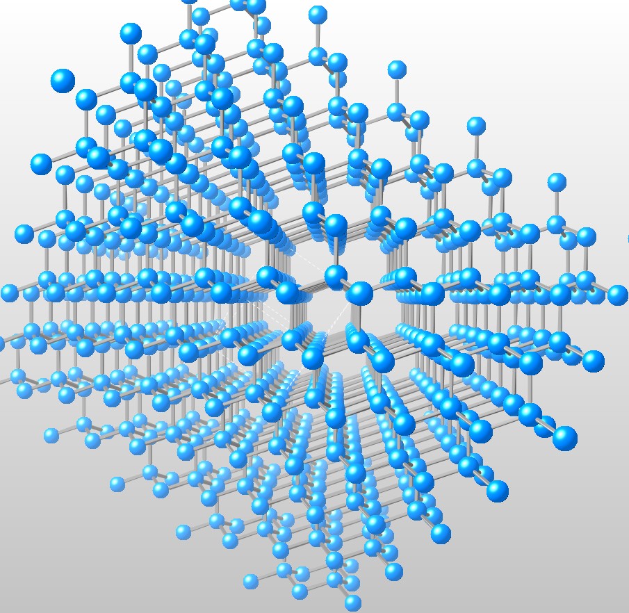
Cite this entry
Böer, K.W., Pohl, U.W. (2018). The Structure of Semiconductors. In: Semiconductor Physics. Springer, Cham. https://doi.org/10.1007/978-3-319-69150-3_3
Download citation
DOI: https://doi.org/10.1007/978-3-319-69150-3_3
Published:
Publisher Name: Springer, Cham
Print ISBN: 978-3-319-69148-0
Online ISBN: 978-3-319-69150-3
eBook Packages: Physics and AstronomyReference Module Physical and Materials ScienceReference Module Chemistry, Materials and Physics