
Abstract
The emphasis of materials analysis using ion beams is directed towards the composition and structure of surfaces and near-surface layers on the depth scale from nm up to μm. Ion beam-based analytical techniques concern with ion sources, ion beams, the kind and cross section of ion interaction with matter, the emerging radiation (e.g., sputtered secondary ions, scattered ions, ion-induced photon, and electron emission), and appropriate radiation detection systems.
Access provided by Autonomous University of Puebla. Download chapter PDF
Keywords
- Target Atom
- Depth Resolution
- Nuclear Reaction Analysis
- Concentration Depth Profile
- Elastic Recoil Detection Analysis
These keywords were added by machine and not by the authors. This process is experimental and the keywords may be updated as the learning algorithm improves.
6.1 Introduction
The emphasis of materials analysis using ion beams is directed towards the composition and structure of surfaces and near-surface layers on the depth scale from nm up to μm. Ion beam-based analytical techniques concern with ion sources, ion beams, the kind and cross section of ion interaction with matter, the emerging radiation (e.g., sputtered secondary ions, scattered ions, ion-induced photon, and electron emission), and appropriate radiation detection systems.
For materials analysis with ion beams there exist a variety of experimental techniques, which are summarized in Fig. 6.1 as an ion mass–ion energy map. As shown in Fig. 6.1, one can divide all methods into three ion energy ranges (1) low-energy range of some keV, (2) medium-energy range of 30–300 keV, and (3) high-energy range of ~0.5–100 MeV. In relation to the primary ion mass, light ions (M < 10, mostly H+, He+) in a wide energy range are used for scattering techniques (LEIS, MEIS, RBS) and particle-induced photon emission techniques (PIXE, PIGE). Heavier ions (e.g., N, O, Cl, etc.) are necessary mainly for the techniques of NRA and ERDA. Low-energy (some keV) heavy ions (M i ≥ M Oxygen) with a certain sputter yield of target atoms are necessary in the widely used analytical technique of secondary ion mass spectrometry (SIMS).

Ion beam-based analytical techniques in relation to primary ion mass and ion energy: SIMS secondary ion mass spectrometry, LEIS low energy ion scattering, MEIS medium-energy ion scattering, RBS Rutherford backscattering, ERDA elastic recoil detection analysis, PIXE particle-induced X-ray emission, PIGE particle-induced gamma-ray emission, and NRA nuclear reaction analysis
Characteristic differences between photon, electron, and ion interactions with matter are illustrated in Fig. 6.2, which compares the radiation range or penetration depth as well as the electron and ion trajectories in silicon obtained by Monte Carlo calculations. Typical X-rays of some 10 keV photon energy exhibit a very deep penetration depth in the mm range with exponential intensity decay by photon absorption. Typical electron energies are some 10 keV, and the interaction range is restricted to some 10 μm. The electron penetration into the solid is characterized by a large longitudinal and transversal straggling (pear-shape profile) and a low-beam damage because of small electron mass. In contrast, medium- and low-energy heavy ion irradiation, for example with 60 keV Ga+ ions, interacts with the solid only in a very shallow depth region of <100 nm with high-target damage and target material removal by sputtering. These interaction processes are of special importance for SIMS. On the other hand, high-energy light ions, for example, 2 MeV He+ used for RBS, cause a deep probe beam of some μm with well-defined depth and collimation (small lateral ion straggling due to weak interactions) and with a small low-damage region of about ~0.5–1.0 μm size located in the Bragg-peak at end of ion range.

Comparison of penetration depth and particle trajectories of radiation in silicon
Compared to many other analytical techniques, including SIMS, ion beam analytical methods with high-energy ions (usually in the literature called IBA) have the advantage that they are nondestructive, easy to use, and provide quantitative interpretation of measurements. The high accuracy of these ion beam techniques is mainly due to the precise knowledge of cross sections of the involved atomic and nuclear processes.
As described in Chap. 2 and schematically shown in Fig. 6.2, ions impinging the target undergo a series of elastic [with nuclear energy loss S n = (dE/dx)nuclear] and inelastic [with electronic energy loss S e = (dE/dx)electronic] collisions with the host atoms until they stop at some depth.
Depending on ion mass M and ion energy E, both ion-stopping processes S n and S e can appear together or one of them dominates [1, 2]. For example, in the low-energy range of 10–200 keV, typical for ion implantation of heavy ions, usually S n is the dominating stopping process. High-energy light ions in the MeV region loss their energy predominantly by electronic stopping S e [3]. As an example, Fig. 6.3 shows the distributions of the nuclear and the electronic stopping over a wide energy range for He+ ions in silicon.

Nuclear stopping and electronic stopping as a function of ion energy for He+ ion irradiation of silicon
At ion beam analysis (IBA) using light ions (H, He) in the 1–3 MeV range, the dominating energy loss is given by the electronic stopping S e = (dE/dx)e as can be seen in Fig. 6.3. Therefore, in the near-surface layer, which is analyzed, no defects are created. From the figure it can be also concluded that only at the end of the ion trajectories in the solid, where the ion energy is slowed down below some keV, nuclear stopping becomes comparable or higher compared to electronic energy loss. Thus, only in these depth regions ion-induced damage occurs, and therefore, RBS is assumed as a nondestructive analysis technique.
Ions accelerated to different energies and entering the target cause different interaction phenomena at both the atomic and the nuclear level leading to the emission of particles or photons with energies characteristic for elements in the target (see Fig. 6.4) [4]. In some analytical techniques, the same incident and emerging ions are employed, as in ion-scattering techniques (e.g., RBS, but also MEIS, LEIS). In other cases, the primary incident ion, the emerging ion, and photon radiation from the target differ, which is indicated as:

Schematic representation of ion–target interaction. MeV ion induced elastic and inelastic interaction processes are related to common ion beam analysis (IBA), whereas primary heavy ions of some keV are used to sputter secondary target ions or atoms which are mass analyzed by SIMS [4]
-
Primary ion in, target ion/atom out: ERDA (and also SIMS)
-
Primary ion in, X-ray or γ-ray out: PIXE or PIGE, respectively
-
Primary ion in, nuclear reaction products out (e.g., protons, deuterons, α-particles, γ-rays, etc.): NRA
Except SIMS, LEIS and MEIS common ion beam analysis of materials requires high-energy ions in some 100 keV and MeV range which are produced by accelerators as described in Sect. 3.6. Accelerator-based high-energy ion beams are in many cases more sensitive compared to other photon and electron-based probe techniques. The reason is that ions carry high momentum and interact more strongly with target electrons and nuclei through Coulomb forces between them. The basics of these ion–solid interactions have been described in Chap. 2.
Elastically backscattered light ions are detected in RBS and elastically recoiled (secondary) target atoms are detected in ERDA. X-rays and γ-radiation emitted from the target give element-specific information due to characteristic photon emission at relaxation of excited electron clouds (X-rays) or of excited atomic nuclei. This information is detected in the analytical methods of particle-induced X-ray emission (PIXE) or particle-induced gamma emission (PIGE), respectively. Nuclear reaction analysis (NRA) is a pure nuclear technique as it is governed by nuclear reactions and kinematics. If the primary ion energy exceeds the Coulomb barrier and the ion penetrates into the nucleus, it performs a nuclear reaction. In NRA, the primary ion is absorbed by the nucleus of target atoms at some resonance energies, and subsequently different secondary particles (proton, deuteron, neutron, or α-particle) or γ-rays are promptly emitted which can be detected. It must be mentioned that, in principle, PIGE is also an IBA technique, which is based on nuclear reactions. The proton (particle)-induced γ-ray emission (PIGE) is restricted to the detection of γ-rays emitted in (p,γ), (p,pγ), and (p,αγ) reactions.
The incident ions interact either with atomic electrons or atomic nuclei of target atoms, as schematically shown in Fig. 6.5. The interaction with an atomic electron is purely Coulomb, and therefore it is governed by Coulomb’s law. The Coulomb interaction of the ion with electrons can eject an electron from an inner orbital (as shown in Fig. 6.5) or excite electrons into higher orbitals. The ejected secondary electrons can ionize or excite further target atoms. In both cases, ionized or excited target atoms decay via emission of characteristic X-rays into their ground state which can be analyzed by PIXE. At high energies sufficient to overcome the Coulomb barrier, the incident ion enters the target atomic nucleus and induces a short living (~10−14–10−18 s) compound nucleus or an excited nucleus. There exist different decay channels through which the compound or excited nucleus returns to its ground state, accompanied by the emission of γ rays (mainly used for PIGE) or secondary reaction particles of 1H (proton), 2H (deuteron), 3He(triton), 4He (α-particle), or neutrons which can be detected in NRA. Additionally, Fig. 6.5 shows schematically a light ion elastically scattered at the target atomic nucleus and a target atom elastically recoiled by the incident ion, which are detected in RBS and ERDA, respectively.

Ion–target atom interaction at relevant IBA techniques
The effects of ion–target atom interactions are summarized in Table 6.1. Nuclei are unaffected in the case of elastic ion scattering and inelastic collision. The interaction force is Coulomb, and the ion only changes its direction (elastic scattering) or is decelerated and causes bremsstrahlung (inelastic collision). If the bombarding ion energy is high enough to negotiate the Coulomb barrier, nuclei of target atoms will be excited. This can be caused by Coulomb excitation and also by inelastic scattering. In the latter process, the interaction force is nuclear. Nuclear interaction forces can also affect nuclear reactions with nucleus transformation.
A special case is the interaction of highly charged ions with solid state surfaces, as schematically demonstrated in Fig. 6.6 [5]. Important results were published by Burgdörfel et al. (e.g., [5–7]). Highly charged ions have a large amount of potential energy, which for slow ions may exceed their kinetic energy. Because of the small surface interaction area of some nm2 and the very short interaction time of some 10−15 s a very high-power flux of 1013 W cm−2 is realized. The ions are accelerated towards the surface (A) and a “hollow atom” will form up (B). At impact with the surface electron emission takes place (C). The relaxation below the surface (D) is accompanied by target modifications and by radiation emission of X-rays and AUGER electrons, which can be used for analytical investigations. However, the use of highly charged primary ions is of minor importance for their application in materials analysis. Nevertheless, they have attracted interest for basic investigations of ion–surface interaction phenomena.

Interaction of highly charged ion with a solid state surface (schematically) [5]
Besides all ion-induced particle and wave radiations mentioned above, secondary ions are also emitted from an ion-bombarded target surface and can be used for analytical aims. For this purpose, the emitted ions are analyzed in a mass spectrometer, and consequently this method is named secondary ion mass spectrometry (SIMS). It is described in more detail in Sect. 6.7. Furthermore, a direct visualization of target surfaces is possible by different ion beam-imaging techniques as field ion microscopy and ion microscopy with stationary or scanning ion beam, respectively. These imaging techniques are the subject of Sect. 6.8.
As described before common IBA techniques (RBS, ERDA, PIXE, PIGE, NRA) concern with ion energies in the usual range of several MeV. Compared to RBS, the two other scattering techniques MEIS and LEIS use ions with energies of 30–300 keV or only of some keV, respectively. For these techniques high-voltage accelerators are not necessary and common ion sources together with appropriate ion extraction or acceleration stages are applied providing the desired ion beams.
Differently, in the other kinds of ion analytical techniques, such as SIMS, only secondary ions emitted from the solid surface are analyzed by their mass. In order to use these methods to determine concentration depth profiles, it is necessary to remove layers with controlled thickness of the sample. This surface layer removal is carried out by surface bombardment with low energy (0.5–20) keV heavy ions with masses M i ≥ M O (O+, Ar+, Cs+, Bi+), which sputter target atoms from the surface. The analysis of secondary ions then can be carried out after each layer is removed to determine the composition of the new surface. The fundamentals and processes of sputtering have been described in Chap. 2. In contrast to IBA methods SIMS and related techniques (e.g., SNMS) exhibit destructive analytical methods.
Consequently, the content of this chapter is divided into two main parts:
-
1.
The description of common IBA methods, namely, ion-scattering techniques in Sect. 6.3, particle-induced photon emission in Sect. 6.4, and nuclear-based IBA methods in Sect. 6.5
-
2.
Low-energy ion beam techniques analyzing secondary light and electron emission in Sect. 6.6, methods based on sputter depth profiling with analysis of secondary ions in Sect. 6.7, and finally ion beam imaging techniques (Sect. 6.8).
6.2 Ion Beam Analytical Techniques: A Survey
Common ion beam analytical (IBA) techniques allow the detection of specific elements in near-surface layers of solids and the determination of their concentration. Furthermore IBA techniques permit the determination of thickness, position, and concentration of individual layers in a multilayer target. Special characteristics of IBA techniques are:
-
Generally nondestructive (except for SIMS)
-
Typically a multielement method
-
Simple and quick sample preparation
-
Microtechnique with small sample quantities (mg) and detection ranges (μm)
Primary ions interact with the surfaces, and subsequently different particle and wave radiations will be emitted from the surface. These beams give characteristic knowledge on the solid state surface, and therefore they are mediator for analytical information.
The different kinds of radiations emitted from a target surface after bombardment with high-energetic primary ions are illustrated in Fig. 6.7. As shown in Fig. 6.7a, the primary ions were mass selected, accelerated up to some MeV, then energy analyzed (charge state) by a second magnet, and focused on the sample surface by a focusing ion lens. Different particle and photon radiations are emitted from the target. Emitted particles are elastically backscattered incidence ions [Rutherford backscattering (RBS) and medium-energy ion scattering (MEIS)], particles from nuclear reactions [nuclear reaction analysis (NRA)] and recoil atoms as forward scattered ions [elastic recoil detection analysis (ERDA)]. Emitted photon radiations are γ-rays [particle induced gamma emission (PIGE)] and X-rays [particle induced X-ray emission (PIXE)]. As shown in Fig. 6.7b, each kind of secondary radiation from the target is detected by radiation specific detection systems using semiconductor detectors (semiconductor Si-, Si(Li)-, Ge(Li)-, HP-Ge detectors), scintillator-PM combinations, Bragg-ionization chambers, MCPs, etc. (see Sect. 3.4.5). Usually the signals from the detectors are electronically amplified and shaped and analyzed in pulse high-multichannel analyzer.

Schematic overview of accelerator-based IBA techniques (a) and radiation detection system arrangement (b) for particle and photon radiations emitted from a target surface during ion–solid interaction
The different emitted radiations and the resulting IBA techniques are summarized in Table 6.2. Often two or more of these techniques are used simultaneously in one experimental setup to obtain additional, complementary information.
Very important preconditions for high-efficient IBA techniques are appropriate ion mass and energy of bombarding ions. These parameters are compiled in Table 6.3. As obvious from this table H+ and He+ are the most frequently used ion beams for hydrogen depth profiling. This so-called light ion ERD analysis (LI-ERDA) is a special case because in a straight forward manner the conventional ion energy detection setup (like in RBS with a simple silicon particle detector, only in forward direction) can be used. However, because the H and He projectile masses are low, other heavier elements cannot be examined simultaneously with hydrogen, since the projectile mass needs to be higher than the mass of recoils. For this purpose, heavy ions are used and the ERDA technique is known as heavy ion ERDA (HI-ERDA), where 16O, 20Ne, 28Si+, 35Cl+,127I, etc. as primary ions with higher energies are used. For RBS with light ions (H+, He+) the incident ion energy must be lower than 2 MeV, because for higher energies non-Rutherford scattering becomes significant. If the projectile is lighter than the scattering target atoms, it can be scattered at all angles between 0 and 180°. However, for the ERDA technique, where the projectile is heavier (M 1) than the target nuclei (M 2), there exists a maximum scattering angle of θ max = arcsin−1(M 2/M 1). If the particle detector is placed at an angle of ϕ > θ max, no scattered projectiles (unwanted) but only recoiled ions/atoms are detected [2].
The capabilities of different ion beam analytical techniques are determined by various technical parameters, such as the number of detectable elements, sensitivity, detection limit, depth localization, and depth resolution. The most important techniques are summarized in Table 6.4.
PIXE and PIGE are IBA techniques typically applied for the investigation of trace elements and composition of bulk materials. They have only poor depth resolution in the range from some μm to some 10 μm, but very high-element sensitivity in the ppm range. Typical problems for RBS, MEIS, LEIS, and ERDA are the determination of thickness and composition of near-surface regions. The detectable elements nearly cover the whole periodic system up to U, and these IBA techniques are characterized by very high-depth resolution between monolayer depth and 10 nm. The detection sensitivity is element dependent and differs considerably. For RBS and MEIS sensitivity is best for heavy elements in light element substrates; it reaches from 10 ppm for U up to 1 % for Li [3, 8]. In contrast, the detection sensitivity of ERDA is limited to about 0.1 %, but all elements from H to U in principle can be detected.
Nuclear reaction analysis (NRA) not only allows the investigation of trace elements (1–100 ppm) with a depth resolution in the nm range, but also isotopic tracing and profiling in near-surface regions, interfaces and bulks are possible.
An example of a schematic setup for combined IBA experiments is illustrated in Fig. 6.8. The target is installed usually on a goniometer (sample tilting and rotation) in the center of an evacuated chamber and bombarded by an incident ion beam, which is focused and collimated to beam spot size of ≤1 mm, or for ion beam microprobes of ≤1 μm. Different particle and photon radiations are emitted by the target and collected by diverse detector systems.

In the present example, silicon particle detectors (SPD) are installed behind and in front of the target. The former one is a SPD for LI-ERDA, whereas the SPD in front of the target is installed for collecting of scattered RBS, MEIS and NRA light particles. The nuclear reaction process also generates γ-radiation (PIGE) which is detected by specially designed γ-ray detectors (large volume HP-Ge detectors or scintillator-PM combination). High-detection efficiency is advantageous for the balance between ion beam-induced target damage and the detectable concentration of the elements of interest. Therefore, a special high-efficient γ-ray detector consisting of a large volume NaI (Tl) or BGO scintillator is applied [11]. PIXE is usually detected by conventional Si(Li)- and Ge(Li)-X-ray detectors or modern silicon drift detectors (SDD), which are also installed in front of the target.
As schematically shown in Fig. 6.8, in the case of combined LI- and HI-ERDA, the full analyzing system for simultaneous detection of light and heavy ions is more complicated. Modern ERD systems consist of a SPD (for light recoils of H and He), a Bragg ionization chamber (BIC) (see Sect. 3.4.5), and/or a time-of-flight-energy (ToF–E) detector for the detection of heavy recoiled ions/atoms [12]. The use of BIC and ToF–E detection techniques was introduced in ERDA for both of recoil mass identification and depth information (depth resolution). The ion beam chopper together with one SPD is installed in the vacuum chamber to monitor and to measure the number of incident ions over the measuring time of IBA. For this purpose the ions of the beam are backscattered periodically from gold-covered-winged wheel rotating through the beam.
All detectors are connected with their specific preamplifiers, amplifiers, and high-voltage supplies. The amplified detector signals are usually converted by analog–digital converters (ADC), and processed with respect to their pulse-heights in multi-channel analyzers (MCA). For the combination of all IBA methods in one vacuum chamber, the samples must be mounted onto the sample holder connected with a goniometer to tilt the sample into position for analysis, that is in backward direction or, alternatively, into position for ERDA analysis in forward direction. The goniometer is also necessary if RBS channeling measurements are performed, which need precise alignment of the sample crystal orientation relative to the direction of the incident ion beam. Most IBA chambers are equipped with a load lock for fast sample transfer.
6.3 Ion Beam-Scattering Techniques
Ion-scattering techniques operate across a large ion energy range, from 1 keV to some tens of MeV, each with different benefits and different aspects that can be investigated with each technique. Compared to other surface analytical techniques, the physics-governing ion scattering is relatively simple. Some of the most common ion beam analysis techniques, as Rutherford backscattering, medium- and low-energy ion spectroscopy as well as elastic recoil detection analysis are based upon the physical principle of binary elastic scattering of energetic ions at sample atomic nuclei (see Chap. 2).
To obtain quantitative information about different elements present at the surface or in the near-surface region of a sample, it is necessary to understand the interaction potentials due to the effects of ion neutralization and scattering cross section. Ion scattering is described by a Coulomb type interaction of the two particles, but only at high energies in the MeV range it can be considered to be purely Coulomb. At low energies, because of the longer interaction times, electron screening must be taken into account. The interaction potential falls off faster than 1/r, with the Coulomb interaction being multiplied by a so-called screening function [(2.22) in Chap. 2].
Because the scattering cross sections can be calculated with good accuracy, the scattering techniques RBS, MEIS, LEIS, and ERDA are standard-free quantitative analytical methods. The measurement of the energy loss of incident ions by energy measurement of outcoming, scattered ions allows information about the depth of scattering events in the sample. The obtainable depth resolution is determined mainly by the energy resolution of the detection system. For example in “standard” RBS, conventional Si particle detectors (SPD) restrict the depth resolution to about 10 nm.
6.3.1 Rutherford Backscattering
Rutherford backscattering is the most frequently used ion beam analysis method [2, 3, 13–16]. The principle of the RBS method is demonstrated in Fig. 6.9.

Physical principle of Rutherford backscattering (schematically)
RBS bases upon the elastic collision between a high-energetic beam (MeV range) of light ions (E 0, M 1, Z 1, typically 4He+) and near-surface atoms of the investigated sample (M 2, Z 2). The energy of the elastically backscattered ions is measured under different backscattering angles Θ with respect to the direction of the incident ion beam by a detector. The measured energy E 1 depends on the mass M 2 of sample atoms and on the depth t where the scattering process takes place. The depth can be determined by the ion energy loss on the way to and from the point of scattering interaction with the target atom. This allows to profile the element concentration and composition of the sample close to the surface.
The element identification of a target atom requires the knowledge of the so-called kinematic factor K. This factor is defined by the ratio between the energies of the primary ion after the collision E 1 and before the collision E 0:
The formula for the kinematic factor K at ion scattering can be derived assuming binary elastic collision of the projectile with the target atom (see Fig. 6.9). Taking into account, conservation of energy and momentum the factor K for an ion (M 1) scattered at an angle θ by a target atom (M 2) can be expressed by the following equation [see also (2.8) in Sect. 2.2):
As can be seen from (6.2), for elastic scattering the kinematic factor K is independent of the incident ion energy E 0 and depends only on the mass ratio M 1/M 2 and the scattering angle θ. Furthermore, K is more sensitive to M 2 at high values of M 2 for larger scattering angles θ and consequently, RBS measurements are often carried out at angles around 170° (maximum of K at θ = 180°). Since the target element identification is made on the basis of the kinematic factor K the backscattered energy E 1 consequently is equivalent to the mass scale (see Fig. 6.10).

Example of RBS spectrum demonstrating high-mass discrimination. Incident ions: 25 MeV 35Cl; target composition: thin layer target of 0.23 nm Bi, 0.33 nm Pr, 0.33 nm Ag, 0.46 nm Y, 0.72 nm Cu, and 1.4 nm Mn on a high-purity Al substrate (taken from [17])
The mass resolution δM at RBS analysis can be derived from (6.1) and (6.2). Two target atoms can be distinguished if their mass difference ΔM 2 causes an energy difference ΔE 1 which corresponds approximately to double energy resolution (FWHM) of the overall detection system:
where δE 1 = (δE 2d + δE 2s )1/2 is the total energy resolution including energy resolution of the detection system δE d and energy straggling δE s. Equation (6.3) indicates that the mass resolution δM 2 decreases with increasing projectile energy E 0 and also for heavier target atoms M 2. For the back scattering geometry with θ ≈ 180°, we get from (6.3)
From (6.4) it follows that for a fixed ratio δE 1/E 0(~0.01) projectile ions heavier than 4He+ will result in a better mass resolution, but δE 1 increases leading to a reduced energy resolution. If the incident ions are heavier than 4He+, the RBS technique is known as heavy ion Rutherford backscattering spectrometry (HI-RBS). HI-RBS differs from conventional RBS by the use of time-of-flight detectors (ToF detectors) with large scattering solid angles instead of common silicon particle detectors. The advantages of using heavier ions (e.g., 12C, 16O, 28Si, 35Cl) are a better mass resolution for heavy target elements and improved mass sensitivity, for example of metal surface contaminants on silicon wafers.
As an example for improved mass sensitivity, Fig. 6.10 shows the high-mass resolution in RBS analysis of a thin layer (overall thickness 3.57 nm) with six different heavy atom masses deposited on a light mass Al substrate [17].
The sample was bombarded with 25 MeV 35Cl ions under a scattering angle of 175°, and backscattered Cl ions were detected by a ToF detector with micro-channel plates. HI-RBS is suited for the analysis of thin surface layers. Compared to conventional 4He-RBS mass and depth resolution at the very surface of the sample can be significantly increased. As demonstrated in Fig. 6.10 even isotopes of Cu and Ag can be resolved.
The common schematic Rutherford backscattering setup is schematically shown in Fig.6.11. An incident ion beam (E 0, M 1) bombards a chemically inhomogeneous thin sample of heavy atoms (atomic mass M h) and light atoms (atomic mass M l < M h). The backscattered energy depends on both the atomic mass of the bombarded sample atoms and the depth of the scattering event (here at the front side and at the backside of the thin layer target). The energy differences between the ions backscattered from the front and the backside are ΔE h or ΔE l, respectively, as shown schematically in the spectrum in Fig. 6.11b.

Principal setup of a Rutherford backscattering spectroscopy (a) with θ the scattering angle, α the ion incidence angle, and β the ion emergent angle with respect to the surface normal. Schematic RBS spectrum of light and heavy target ions at different depths (b)
Depth scale: The signal from an atom at the sample surface will appear in the energy spectrum at a position E 1 = K·E 0 (edges 1′ and 3′ for heavy and light atoms, respectively). The signal from atoms of the same mass in a depth t below the sample surface will be shifted by the amount of energy loss (edges 2′ and 4′ for heavy and light atoms, respectively), while the incident ions pass through the sample, both before [ΔE in(x 1)] and after a collision [ΔE out(x 2)]. Formulas usable in RBS analysis are the following:
The energy of the scattered ions E 1(t) as a function of scattering depth t at the detector entrance is equal to
where x 1 is the path length from the sample surface to the scattering point, x 2 the path length from the scattering point back to the surface, and dE/dx is the specific energy loss (also called stopping power) of the ions over the path lengths. The energy losses are caused by inelastic collisions of the light MeV ions with the electrons of the target atoms (electronic energy loss). The factor S is often called the energy loss factor. In (6.6) K⋅E 0 corresponds to the edges 1′ and 3′ and K⋅E 0 − S⋅t to the edges 2′ and 4′ in the RBS spectrum of Fig. 6.11 for heavy and light atoms in the layer, respectively. At normal incidence of the primary ion beam onto the sample surface, (6.6) simplifies to:
with θ the scattering angle.
For every target atom mass M i (here light M l and heavy M h) with the kinematic factor K there exist separate energy-depth scales in the RBS spectrum (as shown in Fig. 6.12), which can be calculated from (6.6) and (6.7).

Interpretation of the energy loss and depth scale in RBS spectra of a Au–Al–Au thin film multilayer [3]. The RBS spectrum was recorded using 2 MeV He+ ions at normal incidence and a scattering angle of θ = 170°
The mostly used detector in Fig. 6.11 is a Si particle detector with a reverse-biased p-n-junction. Each scattered ion creates electron–hole pairs, the number of which is proportional to the energy of the scattered ion. The induced charge pulses are transformed into voltage pulses and amplified by the detection electronics. A computer switches a multichannel analyzer MCA. Each channel possesses an energy width much smaller than the energy differences ΔE l and ΔE h. So a yield spectrum of backscattered ions in dependence of the ion energy appears (Fig. 6.11b), which is a superposition of scatter events at different atoms in different depth. Both axes in Fig. 6.11b can be calibrated in order to get mass concentrations in relation to scattering elements and scattering depth.
The specific energy loss or stopping power dE/dx represents a mean energy loss <δE> of a large number of ions travelling through the infinitesimal thickness dx. Due to the atomic character of energy loss, an indication of thickness in length units without consideration of the atomic density N i (cm−3) in the analyzed layer is not reasonable. Therefore, in ion beam analysis, the stopping cross-section ε(x) is used, which is given in units of eV cm2. Thus,
which represents the mean energy loss <δE> per crossed atomic areal density N i ⋅Δt.
The interpretation of the energy loss and depth scale is demonstrated in Fig. 6.12, where a 400-nm thick Al layer with ~1 nm Au (≈3 monolayers) deposited on its front and rear side is investigated by RBS [3]. The backscattering spectrum was taken at θ = 170° with 2 MeV 4He+ ions. One can clearly discriminate between the two gold thin layers AuF, AuB and the Al layer. Thus, the RBS spectrum is an overlay of the two depth profiles of gold and aluminum, present in the target material.
The depth resolution δt of RBS is equal to
where δE = (δE 2d + δE 2s )1/2 is the total energy resolution including energy resolution of the detection system δE d and energy straggling δE s.
The yield Y of ions back scattered from a thin layer Δt containing atoms N i and measured by the detector (see Fig. 6.13) is given by

Schematic RBS geometry with normal ion beam incidence showing the scattering angle θ and the solid angle Ω = A/R 2 with R the distance of the detector from the sample for the calculation of the differential cross-section
and depends on the number of incident particles N, the size of the silicon particle detector (solid angle Ω), the number of scattering atoms (atomic areal density N i ⋅Δt), and the probability of scattering (backscatter cross-section σ).
The cross-section σ transforms the coordinate space before scattering into the angle space after scattering. The quotient dσ/dΩ denotes the differential backscatter cross section and is expressed by the well-known Rutherford formula (see also Chap. 2) in the center of mass system,
and in the laboratory system for M 2>>M 1,
The knowledge of the differential backscatter cross section allows the standard-less quantification of elements M i in a thin layer Δt with an areal density of N i ⋅Δt from the measured yield Y i (t) in (6.10). The observed energy spectra are line spectra, where the energy values of the lines are identified by the kinematic factors of the atom masses M i and their intensity (yield) ΔY i by the differential cross section and the number N of incidence primary ions. The corresponding areal densities of target atoms N i
can be measured by RBS with a high-accuracy because N and Ω are known within ≤1 %. The accuracy for the determination of element composition using RBS is in the range of a few percent, typically ≤5 %.
Taking into account the solid angle Ω = A/R 2, one can derive from (6.12) and (6.13) the following expression for the yield (detected back scattered ions):
From (6.14) follows that the Rutherford scatter yield is very forward directed, going as 1/sin4(θ/2), which is advantageously used in HR-RBS detecting forward scattered ions by a magnet spectrometer (see Fig. 6.17). The scatter yield increases with decreasing incident ion energy E 0 proportional to 1/E 20 . Furthermore, (6.14) shows that since dσ/dΩ and therefore Y are proportional to Z 21 ⋅Z 22 /E 20 , the sensitivity increases with increasing Z 1 and Z 2 and decreases with E 0. The increased sensitivity for high-Z 1 incident ions and high-Z 2 target atoms has been demonstrated already in Fig. 6.11.
In the case of compound layers containing more than one element, for example, elements A and B with the chemical formula A x B y , the stopping cross-section ε is determined on a molecular basis ε AxBy assuming Bragg’s rule of linear additivity of elemental ε, namely ε AxBy = x⋅ε A + y⋅ε B. To take a specific example of Co2Si, the stopping cross section is written as ε Co2Si = 2⋅ε Co + 1⋅ε Si. If we are interested in the stoichiometry of compound layers A x B y with thickness t, we have to determine from the RBS spectrum the ratio of the A and B areal densities (N⋅t)A/(N⋅t)B. From (6.13) and (6.14), it follows that
because Z 1, E 0, and the scattering angle θ are the same for the elements A and B. Because RBS is a standard-free analytical method composite surface layers (e.g., silicides, oxides, nitrides, ceramic glasses) and multicomponent metal alloys are investigated by this method to determine their stoichiometry and composition with sufficient accuracy. For example, Fig. 6.14 shows a typical RBS spectrum of a sub-stoichiometric SiO x (x ≈ 1, thickness 200 nm) layer deposited by magnetron sputtering on a glassy carbon substrate (SIGRADUR G®). The sample was analyzed using 1.2 MeV He+ ions at a scattering angle of 160°. As can be seen, the RBS peaks for oxygen and silicon are clearly separated from the light mass carbon substrate. The ratio of the integrated areas of the O and Si peaks directly gives the areal densities, respectively, and the excess Si content or the stoichiometry x can be determined. In the present case, the Si excess was equal to (22.3 ± 0.1) at.% corresponding to a stoichiometry of x = 1.07 ± 0.05.

RBS spectrum of a 200 nm thick SiO x sputter layer deposited on a carbon substrate
In many analytical cases, the samples are crystalline and ion channeling phenomena can occur (see Chap. 2). In the case of normal scattering, the incident ions are scattered randomly because target atoms are also distributed randomly in the target matrix (e.g., amorphous materials). If a crystalline sample is properly oriented with respect to the direction of the ion beam, target atom rows or planes can steer incident ions by means of correlated series of small angle collisions. Chains of atoms in the bulk are then shadowed, and, as a result, the probability of scattering from these atoms is reduced, which leads to reduced and totally different scattering yields Y i from the near-surface in the RBS spectrum. The probability of scattering from sub-surface atoms of crystalline target is reduced by at least one order of magnitude for ions incident along channeling direction. At exact channeling conditions (axial and planar channeling), the scatter yield Y i consists predominantly scattering events from top-surface atoms (only “surface peak” in the RBS spectrum) of a perfect crystal. Channeling-RBS (C-RBS) is well suited for investigations of interstitial impurity atoms and crystal defects introduced by ion implantation into semiconductors as shown schematically in Fig.6.15. C-RBS allows the determination of the degree of impurity activation (atoms on substitutional lattice sites) and defect removal after subsequent damage annealing.

Schematic illustration of channeling RBS: (left) ion channeling and scattering on top-surface target atoms and interstitially located impurity and/or target atoms, and (right) corresponding C-RBS spectrum in comparison with a random spectrum. Ψ and d denote the critical angle for channeling and d the crystal lattice spacing, respectively (see Chap. 2)
Furthermore, C-RBS is very useful and sensitive for the investigation of ultrathin surface layers (monolayer deposition or surface contaminants). As an example, Fig. 6.16 shows C-RBS of an Ag surface which is covered with adsorbed Au monolayers [18]. In the aligned crystal with the <110> axis parallel to the incident ion beam 1.0 MeV He ions penetrate along the <110> axis of (a) a clean Ag (111) surface and (b), (c), and (d) for Au-covered surfaces. Because the gold atoms shadow the underlying Ag atom rows the He ion scattering at inner Ag atoms diminishes. Therefore the Ag surface peak decreases with increasing Au coverage. Besides the Ag peak the Au peak appears, which grows with increasing Au layer thickness, from one (b) to four (d) monolayers.

RBS spectra of a Ag surface covered with Au monolayers [18]
In channeling experiments, the orientation of crystals is precisely carried out by a goniometer such that primary ions incident in alignment with the atomic crystal structure. C-RBS measurements are ideal for providing depth distribution of crystal lattice disorder, thickness of amorphous/amorphized surface layers, location of impurity atoms, as well as strain in heterocrystal and superlattice structures. A survey can be found, for example, in Tesmer and Nastasi [8].
Because modern functional layers and layer systems demand nanometer or even sub-nanometer depth resolution instead of SPDs special magnetic spectrometers are applied [19] to perform high-resolution RBS (HR-RBS).
The principal function of such a spectrometer is illustrated in Fig. 6.17. Charged particles which were scattered from the sample with different momenta pass the field of a dipole magnet and are focused to different positions in the focal plane where a position-sensitive detector is located. As detectors, position-sensitive silicon detectors (Si-PSD) or position-sensitive multichannel plates (MCP-PSD) are used. By this way the problem of energy resolution is converted into a problem of position resolution. At HR-RBS the energy of scattered particles can be measured with an increased accuracy of ΔE/E < 10−3, and the depth resolution reaches values smaller than 1 nm, which is more than one order of magnitude better compared to conventional RBS. However, this value is related only to near-surface regions. Due to energy straggling, the depth resolution rapidly degrades with increasing depth.

High-resolution ion beam analysis
As an example for high-depth resolution ion-scattering analysis, Fig. 6.18 shows a HR-RBS spectrum of a multilayer consisting 5 (0.57 nm Ta0.1Si0.9/5.2 nm Si) on Si. The HR-RBS spectrum was measured in forward direction with 2 MeV C2+ ions at a scattering angle of 35.5° using a magnetic spectrometer of the type as shown in Fig. 6.17. The individual layers are clearly resolved, also because the forward scattering angle increases the path length of both incoming and outcoming ions in the sample [20]. Due to the arrangement of the magnet spectrometer in direction of forward scattering, this technique can be easily applied also to LI-ERDA of hydrogen [14].

High-resolution RBS spectrum of a multilayer 5 (0.57 nm Ta0.1Si0.9/5.2 nm Si) on Si [19]
Finally, RBS measurements can be accomplished using solid alpha particle radiation sources usually made from radioactive actinide isotopes (e.g., 241Am, 239Pu, 252Cf, and others) instead of a 4He ion beam provided by an accelerator. As an example, the concept of Rutherford backscattering was applied as part of the scientific mission of Surveyor VI at its moon landing in 1967 [21]. An alpha particle-scattering detector head was employed on the moon surface for first analysis of lunar soil by bombardment with primary alpha particles emitted from a 242Cm source with an energy of E α = 5.353 MeV. Lunar surface atoms were identified by two particle detectors, measuring the energy of scattered alpha particles and by a proton detector, measuring the energy of protons emitted by alpha particle-induced nuclear reactions. The findings suggested that large portions of the lunar soil resemble basalt in composition [21]. Nowadays, in an improved specification this prototype is still used in space research. One of the main drawbacks of RBS is its relative poor sensitivity for light elements present in a matrix of heavier elements, which is in the range of 1–10 at.% for Z < 20, 0.01–1 at.% for 20 < Z < 70, and 0.01–0.001 at.% for Z > 70. The reasons are (1) the low value of backscattering cross-section σ RBS for light elements which is proportional to Z 2 and (2) the low energy E 2 of ions backscattered from light target atoms. In principle, the sensitivity in Rutherford backscattering analysis can be increased by
-
Increasing the number of probing particles N
-
Increasing the detector solid angle Ω
-
Increasing the detector efficiency
-
Increasing the scattering cross-section σ by using heavier probing ions M 1 and decreasing ion energy E 0 and scattering angle θ, respectively
Rutherford backscattering is a very flexible ion beam analysis method. It allows the successful study of the following problems:
-
Absolute thickness of thin films and surface layers (areal density in atoms cm−2)
-
Element concentration profiles as a function of depth
-
Interdiffusion kinetics of thin films (silicides, metals, oxides, etc.)
-
Analysis of elemental composition in complex materials (phase identification, alloy films, oxides, ceramics, etc.)
-
Highly sensitive detection of surface contaminants (surface and interface contaminants, adsorbates, etc.)
-
Defect analysis in crystalline materials (as after ion implantation and annealing)
-
Quantitative implantation dopant profiles in crystalline semiconductors
-
Quantitative control of total amount of impurities implanted into the materials [measured areal impurity density N⋅t (cm−2) is directly equal to the implanted ion fluence Φ (cm−2)]
-
Quantification of implantation standards necessary for other analytical methods such as SIMS (see Sect. 6.7)
-
Quantitative process control, e.g., composition and contaminants
-
HR-RBS and element mapping with focused incident ion beam
In summary, the mean features of Rutherford backscattering are given in Table 6.5.
6.3.2 Medium-Energy Ion Scattering
Compared to conventional RBS medium-energy ion scattering (MEIS) is performed at lower incident H+ and He+ ion energies in the range of (20–200) keV and with higher resolving detectors (e.g., electrostatic analyzers, magnet spectrometers, and ToF detectors). It is a fairly new technique firstly described by van der Veen [22]. MEIS technique allows quantitative information about sample composition, sample surface, and element concentration depth profiles. The following quantities can be measured by MEIS:
-
Angular distribution of ions backscattered from near-surface regions, giving information about atomic locations with ~10−2–10–3 nm accuracy in the best case
-
Energy distribution of backscattered ions, giving information about atomic composition and about atomic depth distribution with best resolution of ~10−1 nm
Therefore, two types of MEIS spectra are gathered from the experimental data: energy spectra and angular spectra. MEIS offers a superior depth resolution while maintaining the same spectra interpretation as RBS. It is also a quantitative technique because the scattering yields Y i can be measured in absolute units.
Modern research topics which were handled by medium-energy ion scattering are mainly related to depth profiling of ultrathin films, as for application in microelectronics. A special advantage of MEIS is here the information about not deeply buried interfaces with a depth resolution in the monolayer range.
Because of the low energy of scattered ions and demands for very high-depth resolution of the MEIS technique, conventional Si particle detectors as for Rutherford backscattering cannot be applied because of their limited energy resolution. As usual detectors for MEIS special toroidal electrostatic analyzers together with position sensitive detectors were developed [23] which achieve an energy resolution ΔE/E ≈ 10−3. It is schematically sketched in Fig. 6.19.

Schematic setup of a medium-energy ion scattering (MEIS) spectrometer
A collimated incident beam of H+ or He+ ions bombards a target mounted on a goniometer and aligned along specific crystallographic directions. A 6-axis goniometer is used to perform, for example, channeling-in and blocking-out MEIS measurements, which means that the crystal must be aligned along a major crystallographic direction, for both incident beam, and outgoing backscattered ions (so-called double alignment geometry). The principle of these measurements allows, for example, to determine the position of surface atoms with an accuracy of ~0.01 nm. This is due to the restriction of scattering only from top-surface atoms without scattering from underlying substrate atoms. Both the energy and the angle of scattered ions are analyzed simultaneously in a toroidal electrostatic analyzer. The position sensitive detector is an array anode combined with multichannel plates, which convert the ion energy into a proportional amount of electrons. The electrostatic analyzer allows an energy resolution of about 150 eV at a primary ion energy of E 0 = 100 keV and an angular resolution of ~0.3°. The position sensitive detector yields a one- or two-dimensional image, where both the energy and the angle are registered for a certain analyzer voltage, which is stepwise changed to analyze all target masses. The simultaneous analysis of energy and angle of scattered ions allow MEIS to measure atomic mass, depth, and atomic surface structure.
The main application fields of MEIS analysis are:
-
Structure of reconstructed single crystal surfaces
-
Study of surface melting
-
Investigation of composite and alloy surfaces
-
Initial stages of oxide growth (e.g., SiO2 on Si, ZrO2, HfO2 on SiO2)
-
Structure of buried layer interfaces (e.g., strain in epitaxial grown layers with certain lattice mismatch, growth of Ni-, Co-, and rare-earth silicides and germanides)
-
Analysis of the layer-by-layer composition of bimetallic surfaces (e.g., PbSe (111)-, PtNi(111)-, and CuPd(110)-surfaces)
-
Characterization of ultra-shallow pn-junctions in silicon (fluence control, dopant depth distribution, extent and depth of the implant damage in (100)Si)
Furthermore, a rather new research field for MEIS became the study of composition and size of semiconducting and metal nanocrystals [24–26]. As an example for the investigations of surface nanoparticles, Fig. 6.20 demonstrates a typical MEIS spectrum and its interpretation [27]. ZnS and CdSe were deposited on a SiO2 surface layer on a Si substrate forming nanoparticles with different shape and composition. The surface was analyzed with 130 keV H+ ions, and the normalized backscattering yield from surface nanoparticles was measured at a scattering angle Θ = 135°. The open circles depict the measuring points, whereas the colored curves represent results of two different model simulations. For both models, the following assumptions for element areal densities of Cd = 0.10 and Se = 0.12 (×1015 atoms cm−2), and concentration ratio of ZnS:CdSe = 20:1 were made. Furthermore, a C x H y O z -capping layer was introduced in the simulations. As Fig. 6.20 demonstrates the best accordance can be achieved by model II, assuming a mixture of ZnS (or of CdSe in ZnS shells) and CdSe nanoparticles.

Formation of CdSe and ZnS core–shell nanoparticles on a SiO2 surface: MEIS experiment and model simulations (after [27])
In summary, the mean features of medium-energy ion scattering are given in Table 6.6.
6.3.3 Low-Energy Ion Scattering
The energy distribution of low-energy ions (1–8 keV) scattered at some specific angles from a solid surface provides information on the mass and the number of surface atoms from the energy position and magnitude of corresponding peaks in the LEIS spectrum [28]. The scattering technique in this ion energy range has been called low-energy ion scattering (LEIS), ion-scattering spectroscopy (ISS), or noble gas ion reflection mass spectroscopy (NIRMS). The acronym LEIS is preferred since the emphasis is on the low ion energies. In LEIS the analyzed depth is restricted only to a few atom layers as schematically shown in Fig. 6.21.

Schematics of LEIS analysis (a) and of corresponding LEIS spectrum (b) of outermost atomic layer composition
In the case of single crystal, surface structure or atom location information can be derived from scatter shadowing and multiple scattering effects. In the case of scattering low-energy ions, the scattering cross section is different from the Rutherford cross section, as the distance of closest approach of the impinging ion to the target atom R min is rather large. Thus, electronic screening of the interaction between the nuclei is important. The screened scattering potential ϕ(r) (see also Chap. 2) is expressed as
where ϕ C(r) and ϕ e(r) are the potential of target nucleus (Coulomb repulsion) and target electrons, respectively. Φ(r/a) is the screening function, which describes how the Coulomb potential is weakened by the electronic screening. Φ is a function of the reduced distance r/a with a, the screening length, which is characteristic of the ion–target combination. At low ion energies <10 keV, scattering cross sections are of the same order of magnitude as atomic dimensions and increase with decreasing energy. Thus, the ions have a relatively low probability of penetrating beyond the surface, and those which do have even less chance of scattering back. Moreover, the ions which penetrate and undergo multiple scattering at near-surface atoms, have a longer interaction time with the target atoms and can be neutralized [29].
The atomic surface concentration N i can be calculated (in a similar manner as in RBS and MEIS) from the yield of backscattered ions Y i according to
with I p—the primary ion current and e the elementary charge, t—the measuring time, f—an instrumental factor (including detector solid angle, detector efficiency, and analyzer transmission), R—a factor, which includes surface roughness and shielding by neighboring atoms, and η i —the elemental sensitivity factor.
The sensitivity factor includes the differential cross-section dσ i /dΩ (calculated for given scattering potentials) and the fraction of charged backscattered ions Pi+ and is given by
Quantitative surface composition analysis is based on (6.17). However, the elemental sensitivity factor is only known for a few combinations of elements, incident ions, ion energies, and scattering angles [30]. Therefore, quantitative analysis often requires calibration against reference samples with known surface concentrations. The surface sensitivity of LEIS is largely due to the fact that only scattered ions are analyzed. In general, most of the incoming ions are neutralized upon impact. Therefore, knowledge about neutralization is a necessary requirement for the understanding of the sensitivity factor [29].
Different kinds of LEIS instruments have been developed. For a detailed review of experimental setups the reader is referred to [31]. Nevertheless, each setup has the same basic components. A schematic of a LEIS with its basic components is shown in Fig. 6.22a.

In contrast to RBS and MEIS which need high- and low-energy ion accelerators, in LEIS relatively small ion sources are required, resulting in compact analysis tools. The ion source provides ions of noble gases (He, Ne, Ar) in the energy range from 0.5 to 10 keV with a low energy spread of <0.5 % of primary energy. An isotopic clean ion beam can be selected by the ion mass filter (e.g., ExB Wien filter) with a mass resolution of ΔM/M ≤ 0.1. Possible neutrals will contribute to the LEIS signal but not to the current measurement, and therefore it must be filtered out by use of a neutral stop. The neutral stop deflects ions by a small angle onto an aperture located before lenses and collimators, which limit the divergence of the ion beam. The spot size of usually ≈1 mm at the target should be smaller than the acceptance area of the analyzer on the sample. The requirements for the sample manipulator used in composition analysis are less strict than in structure analysis, where at least the angle of incidence and the azimuthal angle must be selected with an accuracy of typically ≤1° for angular orientation. Cylindrical mirror analyzers (CMAs) with external coaxial ion source or with a built-in ion source often used for LEIS are characterized both by a well-defined scattering angle (θ > 90°, Δθ ≈ 1°–2°) and a large azimuthal acceptance angle (ideally 360°). Large Δθ yields a high sensitivity, but at the expense of the energy (mass) resolution. This is different for the double toroidal analyzer (DTA) in Fig.6.22b, where a large energy window is imaged onto a position sensitive detector. Using energy imaging of the DTA parallel ion detection and, therefore, an increased sensitivity by a factor of ~103 have been achieved in comparison to CMA. The acceptance angle of the DTAs, which amounts 1°–4°, gives a high-mass resolution.
For the detection of backscattered ions most LEIS setups use electron multipliers, like channeltrons or a microchannelplate.
For the evaluation of data information recorded by the DTA, quantitative element identification and depth distribution of thin layers can be obtained, with a very high-atomic depth resolution of ≤1 nm. LEIS is able to detect all elements heavier than He. The detection limits obtained so far are in the range ≥1 % of one monolayer for the elements Li–O, 1–0.05 % of one monolayer for the elements F–Cl, and 500–10 ppm of one monolayer for all element heavier than K. Using sputter depth profiling in dual beam mode (Ar, Kr, Cs,… as sputter beam and He, Ne, … as MEIS analyzing beam), for example, ultra-shallow As-doping profiles in silicon can be measured. However, compared to SIMS the detection limit is significant higher.
Finally, two examples will be given showing the high-surface sensitivity and depth resolution of LEIS. Figure 6.23 shows LEIS energy spectra taken with a 3 keV He+ primary ion beam from ZnAl2O4 samples as a characteristic example of mixed oxides (spinel type crystal). As can be seen in ZnAl2O4 (solid line) there is no Zn surface peak since Zn atoms are below the outer surface. The tail from the energy of Zn to lower energies agrees with the ZnO spectrum (dashed line), indicating that Zn atoms are present in the second or deeper layers [33].

LEIS spectra of 3 keV He+ backscattered from ZnAl2O4 (solid line) and ZnO (dashed line) [33]
The example in Fig. 6.24 is related to metal–polymer interfaces which play an important role in the development of organic light-emitting diodes (OLEDs). As shown in this figure, most of Ba diffuses into the polymer already during evaporation of Ba on PPV. From the comparison of the measured peak shape (red line) with the signal from a sub-monolayer of Ba (blue line), a depth of the diffused Ba layer of 7 nm was determined. One of the important problems in development of OLEDs is the minimization of metal diffusion (narrow depth distribution) into the polymer to achieve higher light emission efficiency.

Ba signal in the LEIS spectra of two different poly(phenylenevinylene) (PPV) samples showing Ba present in the outermost layer only (blue line) and Ba additionally present in the bulk (red line) (taken from [34])
6.3.4 Elastic Recoil Detection Analysis
Elastic recoil detection analysis (ERDA) is governed by simple binary elastic collisions between the projectiles and the target atoms like for the other ion scattering techniques (RBS, MEIS, LEIS) described before [3]. The schematic physical principle of ERDA is demonstrated in Fig. 6.25.

Physical principle of elastic recoil detection analysis (ERDA) with θ the scattering angle and φ the recoil angle which is actually the detector angle
ERDA bases on the elastic collision between heavy ions (e.g., O, Cl, I, Ag, Au) with energies in the MeV range and target atoms of the investigated sample (M i , Z i ). Contrary to Rutherford backscattering in ERDA knocked-on or recoiled target atoms are detected in the forward direction, as firstly reported by L’Ecuyer et al. [35].
As incident projectiles usually heavy ions are applied, because in accordance with (6.10)–(6.14) the cross-section σ I and therefore the yield Y i of the recoiled target atoms increase with increasing atomic number Z 1 of primary ions. The energy of target atoms recoiled under the angle φ can be calculated from
with K r the kinematic factor (here energy fraction transferred from primary to recoiled particles). The kinematic factor for the simultaneously scattered primary ions K s is given by (6.2). If the projectile mass, its energy, and the recoil angle remain fixed under a given experimental condition, atoms of different masses M i in the sample come out with different recoil energies E i as governed by (6.19). The kinematic factor K r for ERDA is a function of the mass ratios M i /M 1 and the recoil angle φ. According to (6.19) one can conclude that for ERDA the mass resolution is high at small recoil angles φ (maximum of dK i /dM i at φ = 0). At small angles, also the values K r are large because the energy transfer from the projectile to target atoms is high and the energy spread will be low. This allows to use relatively large detector solid angles Ω compensating at the same time the fact that the differential scattering cross-section dσ/dΩ has its maximum at φ = 90°. In ERDA dσ/dΩ is given by
In contrast to RBS, (6.20) shows that for M 1>>M i the term Z i 2 is compensated by the 1/M i 2 dependence and the sensitivity is roughly constant for most element present in the sample. From the dependence 1/cos3 φ it follows that the recoil cross-section is high for angles close to φ = 90°.
Generally, for ERDA the mass of an incident particle is greater than that of the target atoms. Therefore ERDA is a very convenient analyzing method for hydrogen detection using light 3He or 4He incident ions and, more general, for simultaneous element detection using heavy incident ions M 1>>M i . Usually, ERDA is carried out at very small incidence and recoil leaving angles α and β with respect to the sample surface (glancing geometry). The conversion of measured recoil energies into the depth scale t is given by the energy losses of the incoming projectile and the outcoming recoil or the corresponding energy loss factor S [see (6.5)]. The energy difference ΔE between a recoil from the surface and a recoil from the depth t is given by
where E 2 = K 2⋅E 0 is the energy of the recoil originating from the surface. The energy loss factor S also relates the energy resolution δE to depth resolution δt = δE/S.
As in RBS, the simplest way to use ERDA is the measurement of the recoil yield as an energy spectrum Y(E i ) which contains information about the concentration depth profiles N i (x) within the analyzed layer. However, ERDA is connected with two difficulties (1) The recoil mass M i and the depth t of scattering event cannot unambiguously determined, which is referred as “mass-depth ambiguity” (different masses emerging from different depth can reach the detector with equal E i ). (2) A recoiled target atom M i and a scattered projectile M 1 from different events cannot be unmistakably distinguished, which is referred as “recoil-projectile ambiguity” [36]. Therefore, different elastic recoil detection setups have been developed to solve these problems:
-
1.
Use of absorber foils in front of a common silicon particle detector (SPD) to discriminate heavy-scattered projectiles (resolving recoil-projectile ambiguity) in conventional ERDA for depth profiling of light elements, e.g., hydrogen isotopes [37].
-
2.
Use of time-of-flight (ToF) arrangement to identify recoil masses and scattered projectiles (resolving mass-depth ambiguity) in heavy ion ERDA (HI-ERDA) [38].
According to E i = (1/2)⋅M i ⋅v i 2 with v i = L/t i , where L is the flight path and t i is the flight time, the measurement of the flight time t i allows not only the identification of recoil masses M i but also an improvement of the depth resolution. The relative accuracy of the time measurement δt i /t i can be made much better than the relative accuracy of an energy measurement δE i /E i just by elongation of the flight path L [8].
-
3.
Use of ΔE–E telescope configurations (combinations of a thin, transmissive ΔE–SPD and a thick stop SPD [39] or combination of a transmissive gas ionization chamber (GIC) with a stop SPD [40]).
-
4.
Use of Bragg ionization chamber (BIC, see Chap. 3) as ion mass and energy dispersive detector to resolve both ion masses M 1, M i (from the Bragg peak) and energies of scattered incidence E 1 and recoil ions E i (from the total energy) [41].
At present, in most cases of heavy ion ERDA ToF–E, ΔE–E telescope configurations and BIC detectors are applied. The BIC detector is in principle also a (ΔE–E) ionization chamber which separates recoils only at sufficient high energies (10–100 MeV). In contrast to BIC, in ToF–ERDA works also at lower ion energies of <10 MeV [42, 43].
Using ToF measurements it is possible to identify and separate different masses M i from a two dimensional scatter plot of flight time t i versus energy E i . In the case of recoil measurements by ΔE i –E i telescopes and BIC detectors the masses are identified from a scatter plot of ΔE i versus E i . The advantage of all ERDA detection methods is the simultaneous recording of depth profile for all target elements lighter than the projectile. Therefore a special application field of ERDA is the characterization of elemental composition and depth profile investigation of light elements in heavy element substrates which cannot be detected by RBS [3]. During ERDA in some cases sample damaging by heavy incident ions with high energies can be a problem. Therefore, much lower ion energies are of growing interest because they are much less damaging. The prospects of low energy ERDA are reviewed by Döbeli et al. [43].
As a typical example, Fig. 6.26 shows the ERDA setup at the Helmholtz-Zentrum Dresden-Rossendorf (HZDR), which is installed at the 6 MV-tandem accelerator (6 MV-Tandetron from High Voltage). The ERDA setup combines a ToF–E detector and a BIC detector-analyzing channel for different analytical purposes.

ERDA setup at Helmholtz-Zentrum Dresden-Rossendorf (HZDR), installed at the 6 MV tandem accelerator (6 MV Tandetron from High Voltage)
As characteristic examples, Figs. 6.27 and 6.28 show two-dimensional scatter plots from ToF measurement using a ΔE i –E i telescope with a GIC detector and from recoil analysis using a BIC detector, respectively. Figure 6.27 demonstrates the high-mass resolution (~35) which can be seen from the isotope resolution for B, Si and K obtained from a quartz glass substrate. The measurements were performed using 12 MeV 127I ions under an angle of ~35° of the ToF spectrometer relative to the direction of the incident ion beam.

(a) Two-dimensional scatter plot (ToF–E histogram) from a quartz glass surface obtained with 12 MeV 127I ions using a ToF setup combined with a high-resolution gas ionization chamber (GIC) for energy measurement. (b) Corresponding recoil mass spectrum obtained from the ToF–E histogram (taken from [44])

(a) Two-dimensional scatter plot (ΔE–E histogram) from C–Co composite layer co-sputter deposited at room temperature on SiO2 and subsequently annealed at 300 °C. The spectra were obtained with 35 MeV 35Cl7+ ions using a Bragg ionization chamber (BIC) for ΔE and E energy measurements. (b) Corresponding depth profiles of all elements present in the sample obtained from the ΔE–E histogram [45] [Munnik F (2011) Private communication, unpublished]
The film areal density and composition were obtained from measurements with 35 MeV 35Cl7+ ions impinging at an angle of 15° relative to the film surface. The backscattered ions and the recoils were detected with a BIC detector placed at a scattering angle of 30°. Additionally, a standard Si detector was located at a scattering angle of 38° for hydrogen detection. In this case, an aluminum foil was employed in front of the detector to stop heavier recoils and backscattered 35Cl7+ ions.
Figure 6.28 demonstrates that the ERDA data evaluation of the two-dimensional ΔE i –E i histogram results in depth profiles with sufficient high-depth resolution (~5 nm at the surface and ~10 nm at a depth of 75 nm) for all elements present in an C–Co composite layer deposited on SiO2 [45] (Munnik F (2011) Private communication, unpublished).
For obtaining elemental depth profiles from measured ERDA spectra there exist suitable analysis procedures for which the reader is referred to [46, 47] and available analysis software, e.g., SIMNRA or NDF, referred to [48–50].
A typical example for ERDA application is the measurement of depth profiles in TiAl alloys after ion implantation [51, 52]. Gamma-phase TiAl is an attractive light weight material for advanced applications in aerospace and in power generation plants, e.g., as a material for turbocharger rotors. To overcome its poor oxidation resistance at temperatures above 700 °C, plasma immersion ion implantation of halogens (notably chlorine and fluorine) has been applied. As a result the modified TiAl alloys were protected against environmental oxidation and showed an improved structural and mechanical integrity (see also Sect. 4.8.1) [51].
In Fig. 6.29, the depth profiles of element concentrations in a TiAl alloy are shown, which were measured by ERDA after plasma immersion ion implantation (PIII) of fluorine. As a result it was concluded from the obtained Al and O profiles that fluorine ion implantation initiate TiAl surface passivation at higher temperatures by forming a surface Al2O3 layer. The concentrations of both O and C are minimized in a wide depth region around 100 nm, where the F concentration has its maximum concentration of more than 60 at.%. In Fig. 6.29, the depth resolution of ERDA measuring points is about 10 nm (compare Table 6.7).

ERDA depth profiles in a TiAl alloy after fluorine plasma immersion ion implantation
Special advantages of ERDA compared to Rutherford backscattering are:
-
Depth-dependent chemical composition of samples can be determined which is not possible with RBS
-
In contrast to RBS, where σ ~ Z i 2, in ERDA the cross section depends only slightly on the atomic number and therefore light elements in the target become detectable
-
The scattering probabilities are larger with heavier incidence ions
Deciding disadvantages of ERDA are:
-
The signal of recoiled particles is covered by interfering effects of backscattered incidence and recoiled particles (recoil-projectile ambiguity) and by a background of forward scattered projectiles
-
For the detection of recoiled heavy ions with smaller energies compared to backscattered ones more challenging on the base of time-of-flight arrangements with SPDs or GICs as well as BICs are required
In summary, the mean features of ERDA are compiled in Table 6.7.
For ion beam-assisted nanoscale depth profiling of ultrathin layers with thicknesses of only a few nm, e.g., films deposited by atomic layer deposition (ALD) on semiconductors, high-resolution RBS and ERDA in combination with magnet spectrometers are used [19, 53–55]. From the application point of view in many cases medium- and low-energy ion-scattering techniques (MEIS and LEIS) are increasingly preferred because no accelerators are necessary and these tools can be built in a much more compact manner.
6.4 Ion Beam-Induced Photon Emission
As a result of high-energy ion–solid state interactions, photons are emitted from the target surface which can be analyzed with respect to their energy. The physical principle is schematically demonstrated in Fig. 6.30.

Physical scheme of ion induced photon emission from atomic electron shells (X-ray) or atomic nuclei (γ-ray)
The photon emission results from the interaction between high-energetic (1–3 MeV) light incident ions (usually protons) with the sample atoms. The incident ion can excite electrons of the target atoms or eject them from inner shells of the atoms. During the de-excitation process of the excited target atoms they emit photons with energies of ~(1–30) keV (X-rays). If the energy of the incident light ion is sufficiently high to overcome the Coulomb barrier it enters the target atomic nucleus and induces a short living compound nucleus or an excited nucleus. There exist decay channels through which the compound or excited nucleus returns to its ground state, accompanied by the emission of photons with energies of ~(0.5–10) MeV (γ rays).
The energies of X- and γ-ray photons are characteristic for the target atoms emitting them. The composition of ion-bombarded target samples thus can be determined by measuring the yield and the energy of the emitted photons with a detector. Usually semiconductor Si(Li) or Ge semiconductor detectors are used, and the spectrum is viewed on a multichannel analyzer [3, 56]. In the case of emitted X-rays, the measuring technique is called particle-induced X-ray emission (PIXE), for emitted γ-rays it is called particle-induced gamma emission (PIGE). Since the heavier elements with Z > 11 cannot be detected by PIGE, this method is frequently combined with the PIXE technique.
The ion beam-induced photon emission has some typical advantageous parameters. It allows trace element analysis in bulk materials with sensitivity down to some ppm, a simultaneous multielement analysis of the whole element spectrum (Li–U) and a nondestructive analysis at air with short measuring times. The analysis depth is typically 1 μm. Limitations are the poor depth resolution and missing information about chemical bonding states. Typical investigated materials are metals, glass, ceramics, and biomedical objects.
Recently, some interesting developments were done concerning PIXE and PIGE element mapping with focused MeV ion beams [57, 58]. This was done with the aim of high-resolution biomedical imaging. With conventional PIXE and PIGE element mapping, a lateral resolution comparable with optical microscopy (200–500 nm) could be attained, whereas the best resolution with a direct scanning transmission ion microscopy was ~50 nm [58].
6.4.1 Particle-Induced X-Ray Emission
Particle-induced X-ray emission is an ion beam analysis method which utilizes characteristic X-rays induced via ion beam interactions with the electron cloud of target atoms. The energy of the emitted X-rays is determined by the spacing of the energy levels of the electrons in the atom. This gives rise to a number of characteristic line series (K, L, M, etc.) depending on the final shell. The energy of X-emitted characteristic X-rays depends on the atomic number Z of the target atom. Useful element ranges are for K-series F–Ag, for L-series Cu–U, and for M-series Pt–U. Tables of X-ray energies can be found in reference books or for example on the NIST Web site [59].
Most of PIXE experiments are made with high-energetic protons producing high-energy X-rays with only small absorption along the path from their origin to the sample surface. As a result detections from deep inside of the target—typically in the mm range—are possible [60]. A typical experimental setup for PIXE analysis is shown Fig. 6.8 for samples mounted in a vacuum chamber and in Figs. 7.13 and 7.14 (see Sect. 7.2) for investigations under air using an external ion beam.
The principle of PIXE is comparable with that of energy dispersive X-ray analysis (EDX), where instead of light ions electrons are used as primary particles. However, due to the complete absence of electron induced bremsstrahlung the sensitivity of PIXE is enhanced by a factor of about 100 compared to EDX and is in the order of ppm for most elements [4].
As an example, Fig. 6.31 shows energy spectra of a bronze sample taken by PIXE with 3 MeV protons and by EDX with 20 keV electrons (after [4]). It is evident that by PIXE also minor elements can be identified because of its enhanced sensitivity, which cannot be seen at all in the EDX spectrum.

Comparison of PIXE (red line) and EDX (blue line) spectra taken from a bronze sample. PIXE is generally about 100 times more element sensitive [4]
For PIXE analysis four main physical processes are of importance:
-
1.
The incident charged particle encounters numerous inelastic collisions with the sample atoms
-
2.
The energy of the ion along its trajectory decreases according to the specific energy loss (dE/dx)el (electronic stopping power)
-
3.
Some of the many atoms ionized along the particle path may emit characteristic X-rays with a probability given by the X-ray production cross-section σ
-
4.
X-rays emerging from the point of emission are attenuated by the factor μ in the material
The target composition influences the particle energy loss (dE/dx)el, the X-rays attenuation μ, and the X-ray production probability σ. Generally, the X-ray yield Y i for characteristic X-rays of the ith element in a sample with the thickness t toward the direction of the detector is
where N is the total number of incident ions, N i (x) is the concentration depth profile, σ i is the X-ray production cross section, μ is the X-ray attenuation factor, θ is the X-ray emission angle with respect to the sample surface normal, and β i characterizing the energy loss by the X-rays from the incidence to the detector [9]. In the case that N i (x) is constant (homogeneous bulk samples) and that the X-ray detector has an efficiency ε, the relationship between the observed X-ray line intensity and the element concentration is given by
If both the experiment geometry and the sample matrix composition do not change, K i is independent of the sample. For quantitative PIXE analysis one can either use the approach by calculating K i from X-rays production cross-section σ i , incident ion stopping power S(E), and X-ray attenuation μ, or compare the unknown sample with standards by measuring K i experimentally, which is most often the case. The determination of target element concentrations from the measured yield Y i can be realized with especially developed software packages (see for example [61]).
A typical PIXE spectrum obtained with 2.5 MeV protons is shown in Fig. 6.32 [62]. PIXE measurements were done on a thin Mylar foil which is often used as backing foil for the MicroMatter thin standards (http://www.micromatter.com) for calibration purposes in XRF and PIXE. The Mylar foil contains lots of elements that can affect the correctness of the concentration determination and the system calibration for particular energies. The continuous background with a bump present in the low energy part of the PIXE spectrum is mainly caused by secondary electron bremsstrahlung (SEB). The SEB is caused by electrons ejected from the target atoms by the ionizing proton beam and decelerating in the Coulomb field of other atoms.

PIXE spectrum of a 6.3 μm thick Mylar foil irradiated with 2.5 MeV protons. The spectrum was recorded with a high-resolution silicon drift detector (SDD) [62]
Though most of ions used for PIXE are 2–3 MeV protons, the use of heavy ions (e.g., 3He+, 12C+, 14N+, 16O+) has several particularities. A decisive fact is the higher cross-section σ ion for an incident heavy ion of atomic number Z ion, mass number M ion and energy E ion, compared with that for a proton σ proton:
The cross-section σ ion depends on the velocity (E ion ∝ v 2ion ) and on the square of the ion atomic number (σ ion ∝ Z 2ion ). For example, incident 16O+ ions with an energy of 50 MeV have about the same velocity as 3 MeV protons, but its cross section is larger by nearly two orders of magnitude as compared to the protons. That means that PIXE measurement with 16O+ at 50 MeV requires less data acquisition time by a factor 64 compared to analysis with protons of 3 MeV. Another advantage of high-energy heavy ions as compared to protons is their lower background (bremsstrahlung) in the spectra, especially in the case of light target atoms. This circumstance is particularly advantageous for biological and biomedical samples, which are an object of increasing interest [3].
As an example for such a biomedical application, Fig. 6.33 shows a PIXE spectrum of tumor tissue section of a hamster [63]. PIXE analysis of this tissue section was carried out with a Tandem accelerator based microbeam of heavy 16O ions at an energy of 50 MeV. This kind of PIXE technique has revealed itself as a powerful multielement analytical tool. The ion beam was focused to an area of some μm2, and this so-called Micro-PIXE was successfully utilized for the study of multielement distribution on μm-scale in the tissue section (multielement 2D mapping). As a result of such investigations, for example, the drug copper tetra-phenyl-carboranyl porphyrin (CuTCPH), which was given in discrete doses to a test animal, was found to be inhomogeneously distributed within the tumor.

PIXE spectrum of tumor tissue section of a hamster [63]
In general, heavy ion PIXE leads to more complex element spectra because the electron excitation is more complex and multiple ionization can take place (e.g., X-ray lines are broadened and shifted to higher energies). Moreover, heavy ion PIXE is not yet well established because only a few investigations of cross sections for the K- and L-X-ray production of selected target element-projectile combinations are available. Damaging of the sample by heavy ions can also become a problem.
A wide field for PIXE applications is the study of art objects (see also Chap. 7). As an example, Fig. 6.34 shows the so-called Sky disc of Nebra (left) and the corresponding PIXE spectrum (right) (Neelmeijer C (2008) Sky Disc of Nebra. Private communication, unpublished). The sky disc was found in Nebra (Saxony-Anhalt, Germany) in 1997 and is dated to the bronze age. For each detail on the disc the gold composition was measured in order to clarify whether it belongs to the original design or possibly to a later additive. Furthermore, the Ag/Au and Cu/Au concentration ratios have been used for characterization of the particular gold applications. As a result, the genuineness of the “Sky disc of Nebra” could be definitely confirmed.

“Sky disc of Nebra”. Position for Au analysis with an external proton beam (left) and the corresponding PIXE spectrum (right) [Neelmeijer C (2008) Sky Disc of Nebra. Private communication, unpublished]
Particle-induced X-ray emission (PIXE) is particularly appropriate for analysis of metallurgical (alloys), ceramic, geological (minerals), environmental (pollution analysis) and many other materials, being existent as solids, powders, particularly collected in filter substrates or liquids. PIXE has been increasingly used in biology, medicine, and archeology.
In summary the mean features of PIXE are given in Table 6.8.
6.4.2 Particle-Induced γ-Ray Emission
As has been shown in Sect. 6.4.1, light elements from hydrogen to fluorine cannot be analyzed by PIXE. Depth profiling of light elements in samples consisting heavy elements with RBS is limited because RBS is dominated by the Z-dependence of the heavy element scattering cross-section σ. However, low-Z elements can be detected using nuclear reactions with high-energy ions (under resonance conditions) emitting γ-rays or secondary particles.
The particle-induced γ-ray emission (PIGE) bases on a nuclear reaction between high-energetic (typically some MeV), light incident ions (1H+, 2H+, 3He+, 4He+) and the sample atoms. During the de-excitation process of the excited target nuclei, they emit high-energetic photons (γ-rays), schematically illustrated in Fig. 6.30.
The principal analytical possibilities of PIGE are illustrated in Fig. 6.35. High-energetic incident light ions excite the atoms nuclei of the bombarded sample with an element concentration depth profile N(x). The energies E γ of the γ-rays which are emitted during the de-excitation process are characteristic for the emitting atoms (Z i , M i ). Thus, the element composition of the sample and their depth profiles can be determined by measuring the yield of γ-photons with conventional Ge detectors or scintillators (NaI(Tl), BGO) combined with photomultipliers (see Fig. 6.8). Contrary to PIXE, PIGE does not show continuous sensitivity. Both the energy of the incident ion and the probability of a nuclear reaction are functions of depth determining the γ-reaction cross-section σ γ(E).

Scheme of PIGE analysis
PIGE is often used in conjunction with PIXE for analyzing light elements such as B, Na, Mg, Al, and Si in aerosols and geological samples [64]. PIGE is also used for the light element investigation of art objects as paintings or historical glasses [65].
As an example in Fig. 6.36, the PIGE identification of lapis lazuli pigments in a medieval painting is illustrated. This picture, a Madonna painted by Leonardo da Vinci in 1501, was investigated both with PIXE (heavy elements) and additionally with PIGE (light elements) in order to control its genuineness [66]. The upper PIGE spectrum is taken from original lapis lazuli mineral. It shows a clear Na peak at 441 keV. The spectrum below shows part of virgin’s gown. Here the Na peak has disappeared. The PIXE spectrum of heavy elements of the gown was also modified. These results identify this investigated painting detail to be a restored part.

PIGE identification of lapis lazuli pigments in a Madonna painting of Leonardo da Vinci [66]. Top: original lapis lazuli mineral; below: part of virgin’s gown
Another common application of PIGE is the determination of F in biomedical samples through the reaction 19F (p,p′γ) 19F. The emitted γ-rays have then an energy E γ = 110 keV with a detection limit of 3 × 10⁻⁹ g/cm2 [3].
6.5 Nuclear Reaction Analysis
As the previous IBA techniques, nuclear reaction analysis (NRA) is a nondestructive, isotopically sensitive method with high-mass resolution. NRA is mostly used for light elements analysis (concentration and depth distribution of H, D, Li, B, C, N, O, F, Na, and P). Ions with energies of a few MeV excite the target nuclei and form compound nuclei. At subsequent nuclei decays from the detection of the decay products (usually γ-rays but also particles) absolute impurity concentrations can be determined. Moreover, if crystalline samples are irradiated in channeling direction NRA can be used to determine the lattice location of impurities and the defect distribution depth profile in single crystals. The physical principle of NRA is illustrated in Fig. 6.37 which shows two typical nuclear reactions. Nuclear reaction frequently occurs with light (Fig. 6.37a) and heavier (Fig. 6.37b) incident ions at energies of some MeV, impinging on a sample with light to medium heavy atoms (M i , Z i ) [67]. As depicted in Fig. 6.37 two groups of experimental requirements for NRA exist—first, the detection of emitted light particles (protons and α-particles) by conventional SPDs to measure their number and energy and, second, the detection of emitted γ-rays by Ge-detectors or scintillator/photomultiplier detectors to measure the intensity of photons (see Sect. 6.4.2: PIGE). In the case of particle detection, the depth profiles are obtained from the energy spectra because particles emitted from deeper layers have a lower energy than reaction products emitted from the surface. The concentration is determined from the number (intensity) of reaction particles with a certain energy. At γ-detection only the intensity of photons is measured by detectors arranged usually outside the ion-scattering chamber, which relatively easily allows to enhance the detector efficiency by increasing the solid up to almost 4π [10]. From the counted number of photons, only the concentration of the specific isotope can be deduced. For depth profiling the γ-yield must be measured as a function of the ion energy E 0 for an equal number of incident projectiles (determination of the excitation curve N γ(E 0)).

Physical principle of nuclear reaction analysis (NRA) for two typical reactions: (a) 14N(d,α)12C nuclear reaction with detection of the emitted α-particle for depth profiling of nitrogen, and (b) 1H(15N,αγ)12C nuclear reaction with the detection of the emitted γ-ray for depth profiling of hydrogen
The measured energy spectra E p(x) of emitted particles and the excitation curve N γ(E 0) depend on the concentration depth profile N(x) of the analyzed element and on the nuclear cross-section σ(E(x)) where E(x) is the energy of the projectile at the depth x. The evaluation of the concentration profiles N(x) from E p(x) and N γ(E 0) is simplified for two special behavior types of σ(E(x)):
-
1.
Nonresonant nuclear reaction: σ(E) is constant in an energy interval ΔE and, therefore, the recorded energy spectrum of the reaction particles directly reflects the concentration depth profile in a depth interval Δt corresponding to ΔE (e.g., in the case of the reaction 14N(2H,α)12C in Fig. 6.37a)
-
2.
Resonant nuclear reaction: σ(E) has a strong resonance at in a small energy interval of ~(0.1–1.0) keV around the resonance energy E R and is small for all other energies E < E R < E, which allows to determine the concentration depth profile by measuring the excitation curve N γ(E) (e.g., in the case of the reaction 1H(15N,αγ)12C in Fig. 6.37b).
At nonresonant NRA the depth resolution depends on the stopping powers of incident (dσ/dx)in and emerging ions (dσ/dx)out and the energy resolution of the detector. The depth scale can be obtained from the energy measurement of the emitted particle. The relationship between energy differences ΔE(x) = E(x = 0) − E(x) and depth x can be found, similarly to RBS and ERDA.
In the case of resonant NRA incident ions initially having an energy E 0 are slowed down until the resonance energy E R is reached at depth x, where the nuclear reaction will occur at a rate proportional to the impurity concentration. The depth x and the incident beam energy E 0 are then related by the equation
where θ is the angle between the incident beam and the surface normal, and (dE/dx)in the stopping power for the incident projectile. The yield curve Y γ(x) can be converted into the concentration depth profile by simply changing scales of yield and energy to corresponding scales of concentration N(x) and depth x. The depth resolution δx for resonant NRA is determined by the energy width of the resonance reaction Γ/2, the fluctuation of the projectile energy δE and other statistical fluctuations (Doppler broadening, straggling) and is given by
Typical achievable depth resolutions are ~(1–10) nm in the depth region of (10–2,000) nm, respectively. Therefore, NRA can be used as a high-sensitive depth profiling ion beam analysis technique to measure the concentration and the depth profile of a certain element in a sample with known qualitative composition down to some ppm [68]. Because nuclear reactions are element (isotope) specific for specific incident ions NRA is not able to probe the sample composition of an unknown sample, like in PIXE or RBS.
The nuclear reaction can be represented by the following equation:
with A the incident particle nucleus of mass M 0, X the target nucleus of mass M i , (A + X) the transient compound nucleus, dissociating into C the residual (recoil) nucleus of mass M rec and B the emitted particle with mass M emit, and n·γ the cascade in which n·γ-photons are emitted during the decay process of the excited compound nucleus. Nuclear reactions described by (6.27) are usually expressed in an abbreviated form by X(A, Bγ)C. For different NRA techniques the reader is referred to [8, 69, 70] and for nuclear cross sections to [71]. A summary of common and important 1H, 2H, 3He, and 4He ion induced nuclear reactions used in NRA can be found in [3].
Ion-induced nuclear reactions are suitable for analysis of target elements up to atomic mass 30 (phosphorus). For heavier target nuclei the nuclear reactions diminish due to largely decreased reaction cross sections. The calculation of absolute concentration values is possible with the help of standards and of specific software packages, for example, SIMNRA [72] or SENRAS [73].
As a typical example, Fig. 6.38 shows the NRA setup at the Helmholtz-Zentrum Dresden-Rossendorf (HZDR), which is installed at the 6-MV tandem accelerator (6-MV Tandetron from High Voltage).

NRA setup at Helmholtz-Zentrum Dresden-Rossendorf (HZDR), installed at the 6-MV tandem accelerator (6-MV Tandetron from High Voltage)
For NRA with the setup shown in Fig. 6.38, 1H+, 2H+, 4He+, and 15N+ ion beams with energies in the range of 0.8–10 MeV are mostly used. Usual ion beam currents are in the order of some tens of nA. The γ-rays emitted from the sample are detected with a large area, high-efficiency scintillator (4″ × 4″ BGO) and a photomultiplier.
Some examples for typical NRA investigations with nonresonant and resonant reactions will be shortly described in the following. Figure 6.39 shows measuring results of the deuteron induced nonresonant nuclear reaction 14N(d,α)12C which is often applied to the determination of nitrogen concentration depth profiles of nitride layers (e.g., CVD Si3N4/Si x N y O z layers, or steel surface layers nitrided by ion implantation).

14N depth profiles of a Si3N4/Si/Si3N4 layer stack on silicon (a) and ion implantation profiles in 210Cr46 tool steel (b) examined by the 14N(d,α)12C nuclear reaction at a deuteron energy of E d = 1.4 MeV [74]
The measured implanted nitrogen profiles were found to agree well with N profiles simulated by SRIM (see Fig. 6.39b). For the 14N(d,α)12C reaction the cross-section σ(E) is constant in an energy interval E 0 = (1.0–1.4) MeV and, therefore, the recorded α-particle energy spectrum directly reflects the N concentration depth profile in a depth interval (0–400) nm. For NRA with particle detection deuteron projectiles are more commonly used than proton projectiles [75] if thin surface layers (contamination layers) must be investigated. For example, other useful nonresonant reactions for the determination of C and N are the 12C (d,p)13C and 14N (d,p)15N reactions.
As an example of a proton-induced resonant nuclear reaction, in Fig. 6.40 the results of NRA investigations of a plastic foil are shown [4]. The upper Fig. 6.40a shows the γ energy spectrum of the 19F(p,αγ)16O reaction with a resonance at a proton energy of E 0 = 872 keV. By step-wise increasing of the incident proton energy the depth location of the reaction resonance was successively shifted into the depth of the sample and a depth profile of the fluorine concentration was obtained with a depth resolution in the 10 nm range (Fig. 6.40b).

NRA analysis of a plastic foil using the 19F (p,α γ)16O reaction [4]. (a) γ energy spectrum; (b) F concentration depth profile
Desired or undesired, hydrogen exists in many materials and has a decisive effect on the materials properties. For example, the penetration and inclusion of hydrogen in metals leads to material embrittlement and stability reduction. In a-C:H or a-Si:H, the change of the hydrogen fraction results in altering of electrical, optical, thermal, and tribological properties which at present is an active field of research—with NRA as a powerful tool for such studies.
Besides elastic recoil detection analysis (ERDA), resonant reactions are used for hydrogen depth profiling. The most often used standard resonant reaction for this purpose is the reaction 1H(15N,αγ)12C with a large cross section (see Fig. 6.37b), allowing nondestructive quantitative hydrogen analysis in a solid sample with high sensitivity and depth resolution [76] :
Because of the narrow resonance width Γ/2 of only about 5 keV at a 15N ion energy of 6.385 MeV the depth where the reaction takes place can be varied by changing the incidence energy. Thus, hydrogen concentration depth profiles can be precisely obtained. For incident 15N ion energies of (6.3–12) MeV the analysis depth reaches from the near-surface region up to some μm, with a detection limit in the 10 ppm range and a depth resolution of about 10 nm (for Si in the near-surface region the depth resolution is ~8 nm).
For grazing incidence of the 15N ion beam a hydrogen depth resolution of about 1 nm can be obtained, as demonstrated in Fig. 6.41. Here the hydrogen depth profiles of H2 and N2 annealed thin layers of Al2O3 and of ZrO2 with thicknesses of ~10 nm are shown (Grambole D (2010) Private communication, unpublished). The layers were deposited by Atomic Layer Deposition (ALD) on Si, and as can be seen from Fig. 6.41, hydrogen is mostly accumulated in the region of the interface between the layer and the substrate. After an additional N2 annealing (open measuring points), the hydrogen depth profile in ZrO2 layers remains unchanged, whereas the hydrogen distribution in the Al2O3 layer shifts slightly by ~1 nm to larger depths. At these measuring conditions resonant NRA for hydrogen depth profiling proves to be a very sensitive and accurate method of ion beam analysis.

H depth profiling of Al2O3 and ZrO2 layer by NRA using the resonant reaction 1H (15N,αγ)12C [Grambole D (2010) Private communication, unpublished)
In summary, the mean features of nuclear reaction analysis are given in Table 6.9.
6.6 Ion Beam-Induced Electron and Light Emission
As shown schematically in Fig. 6.5 particle and photon radiations with energies in the keV and MeV region are emitted from a target surface during high-energy ion–solid interactions. To the particle emission also belong electrons, both free and AUGER electrons, which are illustrated in Fig. 6.42.

Emission of electrons and photons by ion radiation of a target atom
Because of the band structure of a bombarded target atom a variety of interactions will take place. The impinging ion may ionize the inner electron shells, if its energy is high enough. The following emission processes are possible:
-
1.
Electron emission: As visible in Fig. 6.42, an ion-bombarded target atom also emits electrons, immediately as free electrons and also in a twice ionized state as AUGER electrons. A further electron emission mechanism for low energy impinging ions of some tens or hundreds of eV energy is caused by their neutralization when approaching the target surface [77]. Yet, because of their low yield and their poor quantification these emitted electrons do not present a competition to analytical techniques with keV electron or X-ray induced electron emission, as for AES or XPS, respectively. Low-energy electrons can be only used for imaging in ion induced Scanning Electron Microscopy (see Sect. 6.8).
-
2.
Photon emission: The wavelength depends on the energy of the impinging ion. For H+ or He+ ions with energies in the MEV range the inner electron shells are excited, whereby characteristic X-rays from the near-surface region are emitted. This X-ray emission is used in PIXE analysis as described in Sect. 6.4.1. For ion bombardment in the keV range, the emitted photons have energies only of a few eV, or with other words, wavelengths from infrared to UV region of the optical light spectrum. One reason for this light emission is a broad band excitation of higher electron levels, but also a recombination of electron–hole pairs exists [78]. As an example Fig. 6.43 shows optical spectra that were induced by the impact of 8 keV Ar+ ions on Cu, Mo, W and Ta surfaces, respectively.
Fig. 6.43 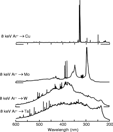
Optical spectra induced by irradiation of Cu, Mo, W, and Ta surfaces with 8-keV Ar+ ions

6.7 Secondary Ion Emission
Besides all ion-induced particle and photon radiations described in Sects. 6.1–6.6, secondary ions are also emitted from an ion-bombarded target surface. These secondary ions can be also used for analytical aims. For this purpose, the emitted ions are analyzed in a mass-selective spectrometer and consequently this method is named secondary ion mass spectrometry (SIMS) [79–81]. One may distinguish between static SIMS and dynamic SIMS. The former one is a nondestructive surface analysis technique with low incident ion current densities, whereas dynamic SIMS is a sputter technique where the sputtered part of the target is immediately used for depth profile analysis of impurities. A similar analytic technique is the Sputtered Neutral particle Mass Spectrometry (SNMS), which analyzes post-ionized neutral particles emitted from the ion-bombarded surface.
Figure 6.44 shows schematically the interaction of relatively low energy primary ions (E 0 = 5–20 keV) with atoms of the bombarded sample surface. Secondary ions (SI) are ejected from the surface by primary collisions of incident ions with target atoms, and also by secondary collision processes of recoiled atoms with target atoms. The primary ion beam produces lattice defects over a depth up to some 10 nm. The SIMS information depth is lower compared to most of IBA techniques and amounts to only few nm. The sputtered material consists not only of SI but also of further neutral and charged particles of the sample material and self-sputtered primary ions. The emitted secondary ions are extracted via an electrical potential and analyzed using a mass spectrometer. Though a semi-quantitative SIMS analysis is possible only by standardization, the detection limit of SIMS is much better than that of comparable depth profile methods. It lies in the ppm range depending on element and materials composition, whereas typical detection limits for AES and XPS are about 10−1 at.%.

SIMS: interactions of primary ions with atoms of the bombarded surface
Basic mechanisms of secondary ion emission are:
-
The sputtering process, which theoretically is well understood
-
The ionization process, which is described by different models, valid only under limited conditions
There exist different possibilities for ionization:
-
Splitting of a surface composition by collision ionization
-
Ionization of neutral emission products just in front (<5 nm) of the surface, as by
-
Electron emission/electron catching
-
Charge exchange
-
-
Auto-ionization from an excited state
The secondary ion (SI) current can be expressed by the following equation:
with I SI the SI current, I P the primary ion (PI) current, S·β+/− the SI yield, S the sputter coefficient, β+/− the ionization state, c the ion concentration of a certain element, and f the transmission factor. The SI yield S·β+/−—generally S·β+—is influenced by both the target atoms and by the primary ions [82].
-
1.
Influence of target atoms: For positively charged SI a high-SI yield is obtained for target atoms with low ionization energy. Especially elements of the main groups Ia, IIa, IIIa, and IVa in the periodic table of elements are characterized by a low ionization energy. The SI yield S·β+ approximately follows the relation
$$ S \cdot {{{\beta }}^{ + }}{{\sim }}\frac{{1}}{{I - \Phi }} $$(6.30)with I the ionization energy and Φ the work function.
For negatively charged SI the yield S·β− depends on the electron affinity of target atoms, which can be expressed by the work function Φ in (6.30). Elements with high-electron affinity are, e.g., Ir, Pt, and Au having a high-yield S·β−.
-
2.
Influence of primary ions: The SI yield β+·S can be written as
$$ {{\rm{\beta }}^{{ + }}} \cdot S{ = }\frac{\rm{SI}}{{{\rm{sputter}}\;{\rm{sum}}}} \times \frac{{{\rm{sputter}}\;{\rm{sum}}}}{\rm{PI}} = \frac{\rm{SI}}{{\rm{PI}}} $$(6.31)that means the number of ejected secondary ions per impinging primary ion.
The diagram in Fig. 6.45 gives the dependence of both values, the sputter coefficient S, and the SI yield β+·S of a Cu target, on the atomic number Z 1 of the bombarding ions.
Fig. 6.45 
Dependence of the sputter coefficient S and the secondary ions yield β+·S of a Cu target on the atomic number Z 1 of bombarding ions

The following results can be deduced from Fig. 6.45:
-
The sputter coefficient S increases with growing Z 1
-
The SI yield β+·S remains nearly constant, that means the ionization state β+ decreases very strongly with growing Z 1
-
β+ varies in a wide range from 10−5 to 1
Generally, the SI yield is a very sensitive value, depending also on the chemical composition of the sample matrix, its atom ionization energy and the surface state (cleanliness, native oxides, contaminants, etc.). Therefore, the SI yield is very sensitive to the presence of oxygen at the surface, as visible from Fig. 6.46. It presenting the SI yield β+·S of different targets with atomic numbers Z 2 at 3 keV Ar+ ion bombardment. The open circles correspond to a clean target surface (10−8 Pa base pressure of the target chamber), and the full circles to values after oxygen adsorption. As can be seen an oxygen adsorption results in an enhancement of the SI yield by a factor 102–103. The usually high demand for surface cleanliness complicates a quantitative analysis of element concentrations by SIMS.

Dependence of the secondary ion yield β+·S on the target atomic number Z 2 for different base pressures in the target vacuum chamber (Ar+ ions used as primary ions)
On the other hand, SIMS offers additional knowledge on the investigated sample:
-
Element ions allow isotopes separation
-
Molecule and cluster ions allow the investigation of chemical compounds
-
By an additional “electron shower” insulators can be neutralized and therefore analyzed
In solid state analysis mainly three application fields of SIMS exist:
-
Depth profile analysis with dynamic SIMS (see Sect. 6.7.1)
-
Surface and thin film analysis with static SIMS (see Sect. 6.7.2)
-
Two-dimensional and three-dimensional element distribution analysis with SI mapping or microscopy (see Sect. 6.8).
6.7.1 Dynamic Secondary Ion Mass Spectrometry (Dynamic SIMS)
For dynamic SIMS primary ions have two functions: they act as an analytical probe and simultaneously they give rise to sample sputtering, which means the sputtered part of the surface is immediately used for depth profile analysis. To produce depth profiles with sputter rates of typically 1 nm⋅s−1 a primary ion current density of about 10–4 A cm−2 is necessary. The depth resolution of a dynamic SIMS depth profile amounts to some nm.
The concentration-depth profile c = f(z) must be evaluated from the measured intensity-time profile I = f(t). Two steps are necessary to obtain the relation c(z):
-
1.
Depth calibration z = f(t)
-
2.
Element concentration calibration c = f(I).
The sputter process itself results in a variation of composition and morphology of the uncovered target surface which must be taken into account to reveal the true profile c = f(z) [83]. The eroded depth z is determined by the sputter rate ż according to
Assuming a constant sputter rate (6.32) can be written as
and the calibration is carried out by a crater depth measurement. The connection of the sputter rate ż with physical parameters of the sputter process is given by (6.34):
with A Pa—particle area on sample surface, d—thickness of a sample monolayer, V m—molar volume (m3 mol−1), N A—Avogadro’s constant (6.022 × 10²³ mol−1), F—Faraday’s constant (9.648 × 10⁴ As mol−1), S—sputter coefficient, M—molar mass (kg mol−1), ρ—density (kg m−3), and j P—IP/A = PI current density.
With typical values for the sputter coefficient (S ≈ 3) and the molar volume (M/ρ = V ≈ 10 cm3/mol) (6.34) can be written in a simple form as an approximated quantitative equation
A supposed primary ion current density of j P = 10–4 A cm−2 results in a sputter rate ż = 1 μm h−1, which is typical for dynamic SIMS. The corresponding values for static SIMS are j P = 10–9 A cm−2 with a resulting sputter rate of ż = 0.01 nm h−1, which means that static SIMS can be assumed as a nondestructive analytical method (see Sect. 6.7.2).
The experimental setup for dynamic SIMS is schematically shown in Fig. 6.47. Because of the surface sensitivity of SIMS the measuring equipment is placed in an UHV target chamber. The primary ions (PI) are generated in a PI source and pass through a magnetic sector field before bombarding the sample surface. The emitted secondary ions (SI) pass through an electrostatic lens system and subsequently they are mass selected in a quadrupole mass spectrometer and detected by a registration unit. SIMS measurement devices are well engineered and commercially available.

Experimental setup of SIMS (schematically)
As an application of dynamic SIMS, Fig. 6.48 shows boron depth profiles after 140 keV (left) and 35 keV (right) boron implantations (fluence 1013 cm–2) into a (100)Si target with and without crystal pre-damage [84]. The pre-damage defects were formed by 60 keV (left) and 200 keV (right) Si+ implantations at fluences of 1013 and 1014 cm–2. The B+ ions incidence direction was nearly parallel to the [85] axial Si crystal channel. The boron range distributions obtained by implantation into an undamaged target are shown for comparison (black lines and symbols). As can be seen, without pre-damaging in both cases pronounced tails of the implanted profiles due to ion channeling were observed. The channeling tails can be suppressed by Si+ implantation with fluences ≥1 × 1014 cm−2. The SIMS data given by symbols were measured by Packan et al. [86]. The described experiment served as a process simulation for a n-MOS transistor structure.

SIMS depth profiles (symbols) for 140 keV (left) and 35 keV (right) boron implantations into a (100) Si target compared with theoretical profiles obtained by Crystal-TRIM simulations (full lines) [84]
As an example for diffusion depth profiles, Fig. 6.49 demonstrates the SI intensity distribution of 28Si+ after Si diffusion from a Si layer into an amorphous FeNbBCu-covering layer [87]. This layer got a thermal pretreatment at 400 °C for different annealing times between 1 and 16 h. According to Fick’s laws progressive Si diffusion into the direction of the surface takes place, as has been confirmed by the SIMS sputter profiles.

SIMS depth profiles of Si diffusion into amorphous FeNbBCu after thermal treatment [87]
As mentioned above an important parameter for quantitative SIMS depth profile analysis is the depth resolution Δz. This resolution is limited not only by the penetration and escape depth of the interacting primary and secondary ions as well as neutrals, respectively but also by ion-induced surface roughening, atomic mixing, and preferential sputtering during surface removal. By an optimization of all these parameters a minimum value Δz < 10 nm can be obtained [88]. Because of the nondirected and low-energetic sputter process a narrow depth resolution function down to few nm is available with plasma SNMS (see Sect. 6.7.3) [89]. In summary, the mean features of dynamic SIMS are drawn up in Table 6.10.
6.7.2 Static Secondary Ion Mass Spectrometry (Static SIMS)
Static SIMS is an established nondestructive surface analytical technique. It is characterized by a very low primary ion current density j P, typically of j P ≈ 10–9 A cm−2. After the approximated quantity (6.34) discussed in Sect. 6.7.1, the resulting sputter rate can be estimated. For j P = 10–9 A cm−2 the corresponding sputter rate amounts to ż = 0.01 nm h−1. Therefore, the removal of the first surface monolayer is a day-long procedure, and so the target surface can be analyzed with static SIMS in a quasi nondestructive manner. For static SIMS the detection limit is in the ppm range relating to about 10–6 monolayers which means a critical mass of ~10–14 g. Because of the low primary ion current density a large surface area must be bombarded for a sufficient confidence level. Therefore the resulting lateral resolution is only in the mm range. This is a significant disadvantage of static SIMS.
A typical static SIMS spectrum is demonstrated in Fig. 6.50. The SI+ emission rate is plotted versus the atomic mass for an ion bombarded Ni–Cr layer on a glass substrate [90]. From the appearance of Si isotopes (28Si+, 29Si+, 30Si+) and alkaline ions one may conclude that no continuous Ni–Cr layer exists. Furthermore, the difficulty of quantification because of element dependence of the SI+ yield is evident. Alkalis and alkaline earths are over-represented, e.g., the peaks of Al and of Na are higher than those of Ni. Therefore, static SIMS spectra need a calibration with standards to obtain (semi-) quantification. Nevertheless, the sensitive detection limit of about 10–6 monolayers is the outstanding advantage of static SIMS in comparison to other surface analytical methods.

Static SIMS spectrum (positive SI) from a Ni–Cr layer on a glass substrate [90]
Because the normally used quadrupole mass spectrometer is unsuitable for the analysis of heavy charged particles as large molecules or ions of heavy metals and alloys, a time-of-flight (ToF) mass spectrometer was developed for use in static SIMS by Benninghoven and Niehuis in 1985 [91, 92].
The mode of operation of such a ToF SIMS device is schematically illustrated in Fig. 6.51 [80]. The target c is bombarded by an electron impact ion source a or by a Ga+ liquid metal ion source b, respectively. All sputtered ions are accelerated to a given potential of some kV, reaching the same kinetic energy. After passing secondary ion optics d the ions drift through a field-free path (length L) with gridless reflectrons e and then strike the detector f.

Mode of operation of a ToF SIMS system (schematically, after [80]) with a an electron impact ion source, b a Ga+ liquid metal ion source, c the target, d the SI optics, e the gridless reflectrons, and f the detector
The measurement of the time-of-flight t of ions with a mass-to-charge ratio m/q provides their mass analysis by
For an exact measurement of the start time the primary ion gun operates in a pulsed mode, and the flight path L must be sufficiently long for a demanded mass resolution of m/Δm ≈ 10,000. An important advantage of ToF SIMS is its possibility of a simultaneous detection of all target masses of the same polarity.
ToF SIMS is meanwhile applied in many research and industrial laboratories because it allows not only spectroscopic information on elemental and molecular surfaces but also the lateral distribution of surface species can be obtained [93]. With a liquid metal ion gun, the lateral resolution of this so-called ToF SIMS imaging is better than 100 nm for elements and in the μm range for large molecules [94]. ToF SIMS has only a small information depth of the first 1–3 atomic layers, connected with a high-depth resolution of <1 nm. Furthermore, it is characterized by a high sensitivity in the range of some 10 ppb [95].
6.7.3 Sputtered Neutral Particle Mass Spectrometry
For SNMS the target is bombarded either with atomic primary ions (O+, Cs+, Ga+, Ar+) or with cluster ions (e.g., Au3+, Bi3+) in the low or medium-energy range (0.2–25 keV). The ion–target interaction predominantly results in the generation of not only neutral particles but also positively and negatively charged ions. Contrary to SIMS in SNMS the neutral particles are the subject of matter [80, 96]. In order to allow the spectrometry of their mass and concentration the sputtered neutral particles are post-ionized just in front of the emitting surface, either by electron impact in low-pressure HF plasma or by interaction with an intense laser beam or an accelerated electron beam. By this way the sputtering and the ionization process are decoupled.
The basic principle of an electron beam post-ionized SNMS is shown in Fig. 6.52 [85]. Sputtered neutral particles (SN) are generated by sample bombardment with primary ions PI and subsequently post-ionized using electrons accelerated to an energy of >50 eV which is higher than that of the first ionization energy for the SN (4–24 eV). The post-ionized emitted particles SN+ are then analyzed in a quadrupole mass spectrometer. An other post-ionization technique was described by Oechsner [97]. Here an inductively coupled HF noble gas plasma, typically Ar, serves for sputtering and then for electron impact post-ionization using the Maxwellian electron gas.

Schematic setup of a SNMS apparatus with post-ionization by accelerated electrons [85]
In comparison with SIMS the Sputtered Neutral particle Mass Spectrometry has some essential advantages. Disturbing matrix effects can be neglected at SNMS because more than 90 % of sputtered material is used for analysis. Furthermore SNMS is suitable for a quantitative or at least semi-quantitative element analysis without standard calibration, because the ionization yield for different elements varies only marginally. This is evident in Fig. 6.53, which shows the element concentrations in a stainless steel, comparatively measured by wet chemistry analysis and by SNMS. Deviations from linearity caused by different ionization probabilities can be neglected.

Certificated element concentrations in a stainless steel related to SNMS signals
An additional advantage of SNMS is the analysis of electrically insulating samples. SNMS measuring values comparable with SIMS exist for the detection limit (10–3–10–4 at.%) and also for the information depth (0.2–2 nm). A disadvantage of SNMS with HF plasma is its poor lateral resolution in the 10 μm range because of the low post-ionization yield resulting in a serious sensitivity limitation. This handicap can be overcome by laser induced post-ionization of neutral secondary particles, allowing nano-analysis down to 50 nm lateral resolution [80].
In spite of the outstanding function parameters of SNMS there exist only few commercial developments, owing to the very complex and expensive equipment. A combined SIMS/SNMS system was developed by SPECS company, Berlin [98]. It bases on fundamental research activities of the group of Oechsner [97, 99–101]. This analytical instrument, called INA-X, offers outstanding features of the SNMS method with electron gas post-ionization. It allows a high sensitivity down to 1 ppm, a high-depth resolution in the nm region and a time efficient depth profile analysis.
The SNMS system INA-X was especially developed for element depth profile analysis with a depth resolution of only a few nm. For this reason it is outstandingly appropriate to thin film investigations. As an example, Fig. 6.54 shows the concentration depth profiles of Fe56Pt/Fe57Pt/Pt multilayers on MgO, after 4 h annealing at 848 K (by courtesy of G. Langer and K. Vad (2006) Private communication, TU Dresden, unpublished). The multilayer preparation was realized by molecular beam epitaxy. Although the single layers have a nominal thickness of only few nm, they are clearly resolved, demonstrating the efficiency of the SNMS technique. In spite of the oscillating concentration of 56Fe and 57Fe the Pt concentration remains constant, and the sum of all element/isotope concentrations amounts to 100 % as an evidence for typical (semi-) quantitative SNMS depth profile analysis.

SNMS concentration depth profiles of Fe56Pt/Fe57Pt/Pt multilayers on MgO [Langer G, Vad K (2006) Private communication, TU Dresden, unpublished]
6.8 Ion Beam Imaging Techniques
A direct visualization of targets and their modification under ion irradiation is possible by different ion beam imaging techniques. One can distinguish between the following techniques:
-
Field ion microscopy
-
Ion microscopy with stationary beam
-
Scanning ion microscopy
All these methods not only allow the acquisition of sample surface images, but also of element distribution patterns with ions. For this purpose, an advanced type of the field ion microscope, the so-called field desorption microscope or atom probe, is utilized [102].
6.8.1 Field Ion Microscopy
The field ion microscope (FIM) represents a microscope that can be used to image the arrangement of single surface atoms on a sharp tip. It was developed by Müller et al. [103]. The physical principle is given in Fig. 6.55.

Physical principle of field ion microscopy (FIM)
To the sharp tip (radius r = 10–100 nm) prepared from the specimen a positive high voltage U tip ≈ 10 kV is applied and the tip is cooled to a cryogenic temperature below 100 K. The specimen is placed in an ultrahigh vacuum chamber which is backfilled with He or Ne as an imaging gas. The gas atoms are firstly polarized and then ionized in front of the tip because of the strong electric field. The hopping and ionization process of the polarized residual gas atoms (here He) in the electric micro-field of the tip is illustrated in Fig. 6.56.

The ionization process of a polarized He gas atom in front of the FIM tip
Unlike conventional microscopes where the spatial resolution is limited by the diffraction of imaging particles or waves, according to Abbe’s equation the FIM is a projection type microscope with atomic resolution. Therefore, the useful magnification, which is the ratio of the screening radius to sample radius, amounts to more than 106. This is illustrated in Fig. 6.57, where the FIM image of a Pt monocrystalline tip with a magnification of 700,000 is given [104]. The visible equipotential lines mark the positions of individual atoms.

FIM image of the tip of a Pt monocrystal (magnification ≈ 700.000:1) [104]
A further actual development of the field ion microscope is the field desorption microscope, where atom desorption from the tip by high voltage impulses U imp or by laser pulses takes place. In a combination with a time-of-flight (ToF) mass spectrometer this microscope is called atom probe. It was already developed by Müller et al. in 1967 [105]. The desorbed atoms fly through a drilled hole in the channel plate of the field desorption microscope into a ToF mass spectrometer (length L) and after it on a single atom detector. The mass m of each desorbed atom can be determined from the time-of-flight τ by
Per 100 pulses about 1 atom is field evaporated and the desorption of atom layers takes place with about 10 pulses per second. Desorption images can be taken as difference images before and after atom desorption via mass spectra of certain elements. As an example, Fig. 6.58 shows the 3D-visualization of individual desorbed atoms from a Cu/(Ni–Fe) multilayer system on a W substrate [106]. At closer inspection horizontal lattice planes in Cu are visible. Modern atom probe instruments with large detector areas allow the measurement of some millions of atoms. This relates to the detection and imaging of a volume of about 100 nm3.

Atom probe image of a Cu/(Ni–Fe) multilayer system on a W substrate with lateral resolution in the nm range [106]
Chemical short range order can be determined by lateral preselection with a narrow diaphragm in the field desorption microscope. By this way an area of few nm2 can be investigated. As an example, in Fig. 6.59, the element distribution analysis of two neighboring areas in a WC–Co hard metal tip is depicted. Figure 6.59a shows the element distribution at a grain boundary between WC and Co, whereas in Fig. 6.59b the element distribution in a WC grain in a distance of only 2 nm is demonstrated. Both spectra are similar, but in Fig. 6.59b the Co2+ peak is missing, which means there exist very sharp concentration profiles at grain boundaries.

Atom probe spectra of element distributions in a WC–Co hard metal tip; (a) at a grain boundary; (b) in a WC grain, 2 nm distant from (a)
An interesting application area of field desorption microscopy is the investigation of short range order by means of desorption spectroscopy, in order to study nucleation processes in amorphous metals. This shall be demonstrated for the metallic glass Fe40Ni40B20. Its exact composition was determined to be
-
77.4 at.% metal atoms (Fe + Ni), called “A”
-
22.6 at.% metalloid atoms (boron), called “B”
The consecutive desorption of both “A” and “B” atoms was registered as a function of time by a data chain on the detector. For example, a part of this data chain is given here as:
AAABABBAAABAABAABABBAAAAABBABBAAAABAAAAAABBBABABBA… The relative frequency distribution of consecutive desorption of two metal atoms n A–A, two metalloid atoms n B–B, or a metal atom followed by a metalloid atom n A–B or contrariwise n B–A is calculated and then compared with the statistic values of a totally disordered amorphous state. The results are given in Table 6.11.
The excellent accordance between measured and statistic frequencies confirms a statistic disordered lateral distribution of metal and metalloid atoms in the amorphous metallic glass Fe40Ni40B20. Therefore, nanocluster formation as an early nucleation state was not found.
6.8.2 Ion Microscopy with Stationary Ion Beam
A stationary microscopic image with secondary ions, emitted from a sample surface, can be received with ion imaging units combined with an ion–electron conversion system. Such stationary ion beam microscopes are manufactured by several companies. The schematic setup is shown in Fig. 6.60.

Schematic setup of an ion microscope with a stationary ion beam
Secondary ions (SI) are emitted from a sample surface bombarded with primary ions (PI). The SI are deflected in an analyzing magnet and reflected by an electrostatic mirror, where ion energy selection takes place. After this the SI pass a projection lens and impinge on an ion–electron transducer. The generated electrons permit the imaging by means of a scintillator together with a photomultiplier. The lateral resolution of these ion microscope images is somewhat better than 1 μm.
An application example of this imaging technique is demonstrated in Fig. 6.61. It shows a three-dimensional (3D) imaging and retrospective depth profiling of layers on a substrate. The 3D-imaging is an exciting technique for the characterization of surfaces and thin layer structures. It is the result of composition of sequential lateral 2D-images. Figure 6.61 illustrates the lateral and depth distribution of 2 μm Al lines (blue) on a photoresist [107]. The vertical image is reconstructed from 64 sequential lateral images and is displayed in a rainbow color scale. The lateral image shown in Fig. 6.61 is the seventh one in sequence from the surface, corresponding to a depth of 2 nm.

Three dimensional ion microscopic imaging and retrospective depth profiling of 2 μm Al lines on a photoresist [107]
6.8.3 Scanning Ion Microscopy
In the broadest sense, a scanning ion microscope (SIM) is an ion beam microprobe for the determination of lateral element distributions and/or depth profiles up to some μm by means of several ion beam analyzing methods, as PIXE, RBS, ERDA, NRA, or scanning microscopy with an incident ion beam, where the image is produced either with ions or with ion induced electrons. In this section the subject of matter shall be limited to the last-mentioned method of ion beam imaging techniques.
A scanning ion microscope (SIM) has a similar setup as a scanning electron microscope (SEM) or—in the case of very thin samples—as a scanning transmission electron microscope (STEM). It was firstly described in 1974 by Levi-Setti [108]. The principle of such a scanning transmission ion microscope (STIM) is schematically illustrated in Fig. 6.62. The essential difference to SEM and STEM is the use of an incident high-energy ion beam instead of an electron beam, which is scanned across the sample pixel by pixel and focused on the sample down to the sub-nm range. In the backscattered mode two detectors are arranged: an ion detector for RBS and a SE detector for ion-induced secondary electrons. For very thin ion-transparent samples (transmission mode) STIM detectors are placed for the detection of transmitted ions in the axial mode and optionally for the detection of ions or ion-induced electrons in the off axis mode. In comparison with SEM with electrons as incident particles the incident focused ion beam produces a smaller interaction area at the sample surface resulting in a higher lateral resolution (δ < 1 nm) and an improved material contrast imaging (see Fig. 6.2).

Physical principle of a scanning transmission ion microscope (STIM)
Scanning ion microscopes work either with ion sources providing high-energy ions in the MeV range [109] or with ion sources supplying He+ ions with energies in the 100 keV range [110]
Some key specifications of the world’s first commercially available Helium scanning ion microscope ORION, manufactured by Carl Zeiss SMT [111, 112] are summarized as following:
-
Probe size of incident ion beam 0.75 nm at 1 pA ion current
-
Field of view down to 100 nm diameter
-
Useful magnification up to 1,000,000
-
He gas field ion source
-
2 electrostatic lenses column
-
5-axis motorized sample stage
-
Everhart-Thornley and microchannel plate detectors
The probe size of the incident ion beam is limited by the He ion source. The principle of an atomic field ion source is schematically shown in Fig. 6.63. By the sharpening process of a metallic needle, individual atoms are stripped away until an atomic pyramid is created just with three atoms at the tip. Under an extremely high electric field He gas atoms are attracted to the tip and ionized in the electric field of single atoms. The emerging ion beam has a very small size and a high brightness, producing a small probe size of <1 nm. This is evident from the FIM image of atoms at the end of the source tip emitting the He ions. Since each tip atom can be individually observed, the source size must be even much smaller [111].

Principle of an atomic-size He field ion source and the associated FIM image of the source tip [111]
The improved material contrast of SIM in comparison with SEM is evident in Fig. 6.64. The picture in the left shows the SEM image of metal interconnect lines in a silicon integrated circuit with contaminants causing short-circuit fault. In the SEM image it is hard to determine if the bridging material is the same or different from the substrate. The SIM image in the right picture clearly shows that the bridging material is different from the metal interconnecting lines because of its vastly different secondary electron yield as compared to the surrounding substrate material.

Semiconductor circuit surface with contaminants causing short-circuit fault (left: SEM, right: SIM) [111]
Furthermore, scanning ion microscope images show a superior depth of focus. It is inversely proportional to half angle of incident beam, which for SIM is typically 20 times smaller than for a SEM. As an example, Fig. 6.65 shows a SIM image of ion-induced SE emitted from an eutectic alloy of Pb, Sn, In, and Bi [111] impressively demonstrating the superior depth of focus of scanning ion microscopes.

Ion induced SE image of an eutectic alloy of Pb, Sn, In, and Bi [111]
References
Meijer J, Vogel T, Burchard B et al (2006) Concept of deterministic single ion doping with sub-nm spatial resolution. Appl Phys A 83:321–327
Hellborg J, Whitlow HJ, Zhang Y (2009) Ion beams in nanoscience and technology. Springer, Heidelberg
Verma HR (2007) Atomic and nuclear analytical methods. Springer, Berlin
Döbeli M (2001) Lecture materials analysis. CERN Accelerator School, Pruhonice
Winter HP, Aumayr F (2002) Slow multicharged ions hitting a solid surface. Europhys News 33:215–217
Winter HP, Burgdörfer J (2007) Slow heavy-particle induced electron emission from solid surfaces. Springer, Berlin
Burgdörfer J, Lerner P, Meyer FW (1991) Above-surface neutralization of highly charged ions. Phys Rev A 44:5674–5685
Tesmer JR, Nastasi M (1995) Handbook of modern ion beam materials analysis. MRS, Pittsburgh, PA
Breese M, Jamieson DN, King PJC (1996) Materials analysis using a nuclear microprobe. Wiley, Chichester
Breese M (2001) Lecture PC 4250 advanced analytical techniques. National University, Singapore
Rohmann D (2009) Mail Portal RUBION. Ruhr-Universität Bochum
Groleau R, Gujrathi S, Martin J (1983) Time-of-flight system for profiling recoiled light elements. Nucl Instrum Methods 218:11–15
Inouye A, Yamamoto S, Nagata S et al (2008) Hydrogen behaviour in gasochromic tungsten oxide films. Nucl Instrum Methods Phys Res B 266:301–307
Kimura K, Nakajima K, Suzuki M (2006) High resolution RBS for nano CMOS applications. Nano CMOS 2006:89–109
Lanford WA, Bedell S, Amadon S et al (2000) Characteristics of Albany’s compact high resolution magnetic spectrometer. Nucl Instrum Methods Phys Res B 161–163:202–206
Nakajima K, Okura Y, Suzuki M et al (2004) Charge-state distribution of 400 keV He ions scattered from solids. Nucl Instrum Methods Phys Res B 219–220:514–518
Döbeli M et al (1990) Heavy ion backscattering analysis with a time-of-flight detector. Nucl Instrum Methods Phys Res B 47:148–154
Feldman LC (2006) Fundamentals of ion channeling. Script Lecture II, Pan-American Summer School “Ion Beams for the Nano Era”, Buenos Aires (02/2006)
Grötzschel R, Klein C, Mäder M (2004) RBS with high depth resolution using small magnetic spectrometers. Nucl Instrum Methods Phys Res B 219–220:344–350
Kimura K, Joumori S, Oota Y et al (2004) High resolution RBS. Nucl Instrum Methods Phys Res B 219–220:351–357
Turkevich AL, Patterson JH, Franzgrote EJ (1968) Chemical analysis of the moon at the surveyor VI landing site. Science 160:1108–1110
Van der Veen JF (1985) Ion beam crystallography of surfaces and interfaces. Surf Sci Rep 5:199–288
Tromp RM, Copel M, Reuter MC et al (1991) A new two-dimensional particle detector for a toroidal electrostatic analyser. Rev Sci Instrum 62:2679–2683
Sortica MA et al (2009) Characterization of nanoparticles through medium-energy ion scattering. J Appl Phys 106:114320–114321
Matsumoto H et al (2010) Au/Pd structures analyzed by high-resolution medium energy ion scattering. Nucl Instrum Methods Phys Res B 268:2281–2286
Gustafson J, Haire AR, Baddeley CJ (2011) Depth-profiling the composition of bimetallic nanoparticles using medium energy ion scattering. Surf Sci 605:220
Goncharova L, Gustafsson T (2008) Preparation and characterization of CdSe semiconductor films. Lecture MRS meeting 2008, Section D
Brongersma HH, Buck TM (1978) Low energy ion scattering (LEIS) for composition and structure analysis of the outer surface. Nucl Instrum Methods 149:569
Brongersma HH et al (2007) Surface composition analysis by low energy ion scattering. Surf Sci Rep 62:63
Brongersma HH et al (1998) A round robin experiment of elemental sensitivity factors in LEIS. Nucl Instrum Methods Phys Res B 142:377–386
Rabalais JW (2003) In: Desiderio DM, Nibbering NMM (eds) Principles and applications of ion scattering spectrometry. Wiley, New York
Brongersma HH et al (1992) Developments in low energy ion scattering from surfaces. Nucl Instrum Methods Phys Res B 68:207
Brongersma HH, Groenen PAC, Jacobs JP (1994) Science of ceramic interfaces. Mater Sci Monogr 81:113
Brongersma HH (2011) Unique surface analysis symposium, Lehigh University, March 23 2011, Bethlehem, PA
L’Ecuyer J et al (1976) An accurate and sensitive method for the determination of the depth distribution of light elements in heavy materials. J Appl Phys 47:381–382
Hofsäß H (1996) Forward recoil spectrometry. Plenum, New York
Pretorius R, Peisach M, Mayer JW (1988) Use of absorber foils in front of a common Si particle detector to discriminate heavy scattered projectiles in conventional ERDA. Nucl Instrum Methods Phys Res B 35:478–483
Thomas JP et al (1983) High resolution depth profiling of light elements in high atomic mass materials. Nucl Instrum Methods 218:125–128
Arnold Bik WM, de Laat CTAM, Habraken FHPM (1992) On the use of a ΔE-E telescope in elastic recoil detection. Nucl Instrum Methods Phys Res B 64:832–835
Stoquert JP, Guillaume G, Hage- Ali M (1989) High resolution recoil spectrometry for separate characterization of Ga and As. Nucl Instrum Methods Phys Res 44:184–194
Assmann W (1992) Ionization chambers for materials analysis with heavy ion beams. Nucl Instrum Methods Phys Res B 64:267
Grigull S et al (1997) Element-dependent ERDA probing depths using different detection systems. Nucl Instrum Methods Phys Res B 132:709–717
Döbeli M et al (2005) ERDA at the low energy limit. Nucl Instrum Methods Phys Res B 241:428–435
Kottler C (2005) Dünnschichtanalyse mittels Vorwärtsstreuung bei tiefer Energie. PhD thesis, ETH Zürich, 16079
Abrasonis G et al (2008) Soft X-ray absorption and emission spectroscopic investigation of carbon and carbon: transition metal composite films. J Phys Chem C 112:17161–17170
Schietekatte F (2008) Fast Monte Carlo for ion beam analysis simulations. Nucl Instrum Methods Phys Res B 266:1880–1885
Arstila K, Sajavaara T, Keinonen J (2001) Monte Carlo simulation of multiple and plural scattering in elastic recoil detection. Nucl Instrum Methods Phys Res B 174:163–172
Mayer M (2002) Ion beam analysis of rough thin films. Nucl Instrum Methods Phys Res B 194:177–186
Barradas NP et al (1999) Unambiguous automatic evaluation of multiple ion beam analysis data with simulated annealing. Nucl Instrum Methods Phys Res B 149:233–237
Jeynes C et al (2003) Elemental thin film profiles by ion beam analysis using simulated annealing – a new tool. J Phys D Appl Phys 36:R97–R126
Donchev A, Richter E, Schuetze M et al (2006) Improvement of the oxidation behaviour of TiAl alloys by treatment with halogens. Intermetallics 14:1168–1174
Donchev A, Kolitsch A, Schuetze M et al (2009) Plasma-immersion-ion-implantation. Plasma Process Polym 6:434–439
Kimura K, Mannami M (1996) RBS single monolayer resolution. Nucl Instrum Methods Phys Res B 113:270–274
Vieluf M (2010) Hochauflösende RBS zur Untersuchung von ZrO2-Schichtwachstum im Anfangsstadium. PhD thesis, Technical University Dresden
Dollinger D et al (1998) Elastic recoil detection with single atomic layer depth resolution. Nucl Instrum Methods Phys Res B 136–138:603–610
Johansson SAE, Campbell JL (1988) PIXE – a novel technique for elemental analysis. Wiley, Chichester
Ren M, van Kan JA, Bettiol AA et al (2007) Nanoimaging of single cells using STIM. Nucl Instrum Methods Phys Res B 260:124–129
Whitlow HJ, Ren M, van Kan JA et al (2007) Characterization of beam focus quality in biomedical nuclear microscopy. Nucl Instrum Methods Phys Res B 267:2149–2152
Mayer JW, Rimini E (1977) Ion beam handbook for material analysis. Academic, New York
Nastasi M, Clarke DR, Suresh S (1996) Ion-solid interactions: fundamentals and applications. Cambridge University Press, Cambridge
IAEA-TECDOC-1342 (2003) Intercomparison of PIXE spectrometry software packages
Kudejova P (2005) Two new installations for non-destructive sample analysis: PIXE and PGAA. Dissertation thesis, Universität zu Köln
Stoliar P, Kreiner AJ, Debray ME et al (2004) Microdistribution of BNCT-compound. Appl Radiat Isot 1:771–774
Ariola V, Campjola L, D’Alessandro A et al (2002) Aerosol characterization in Italian towns by IBA techniques. Nucl Instrum Methods Phys Res B 190:471–476
Schramm HP, Hering B (1989) Historische malmaterialien und ihre identififierung. Lecture ADVA, Berlin
Mando PA (2004) Particle accelerators in art and archaeology. Lecture International School on Written Records, 17 Apr 2004, Erice, Italy
Isobe Y, Sobue K, Ochiai K et al (2000) Analysis of deuterium and lithium on titanium surface by NRA method. Nucl Instrum Methods Phys Res B 170:171–179
Torri P, Keinonen J, Nordlund K (1994) A low-level detection system for hydrogen analysis. Nucl Instrum Methods Phys Res B 84:105–110
Amsel G, Lanford WA (1984) Nuclear reaction techniques in materials analysis. Ann Rev Nucl Part Sci 34:435–460
Lanford WA (1992) Analysis of hydrogen by nuclear reaction and energy recoil detection. Nucl Instrum Methods Phys Res B 66:65–82
Jarjis RA (1979) Nuclear cross section data for surface analysis. Department of Physics, Schuster Laboratory, University of Manchester
Mayer M (1996) SIMNRA: simulation of RBS, ERD and NRA spectra. http://www.rzg.mpg.de
Vizkelethy G (1990) SENRAS: simulation program for nuclear reaction analysis. Nucl Instrum Methods Phys Res B 45:1–5
Neelmeijer C, Grötzschel R, Hentschel E et al (1992) Ion beam analysis of steel surfaces modified by nitrogen ion implantation. Nucl Instrum Methods Phys Res B 66:242–249
Pellegrino S, Beck L, Trouslard PH (2004) Differential cross-sections for nuclear reactions 14 N (d, p)15 N. Nucl Instrum Methods Phys Res B 219–220:140–144
Laube M, Rauch F (1995) Ion beam analysis of temperature induced changes in the composition of float glass surfaces. Nucl Instrum Methods Phys Res B 99:436–439
Hagstrum HD, Becker GE (1967) Ion-neutralization spectroscopy of copper and nickel. Phys Rev 159:572–586
Wünsch G (1976) Optische Analysenverfahren zur Bestimmung anorganischer Stoffe. Sammlung Göschen, De Gruyter, Berlin
Düsterhöft H, Riedel M, Düsterhöft BK (2001) Einführung in die Sekundärionenmassenspektroskopie. Teubner, Leipzig
Bubert H, Jenett H (2002) Surface and thin film analysis. Wiley-VCH, Weinheim
Wetzig K, Schneider CM (2006) Metal based thin films for electronics. Wiley-VCH, Weinheim
Wilson RG, Stevie FA, Magee CW (1989) Secondary ion mass spectrometry: a practical handbook. Wiley, New York
Hofmann S (2004) Practical surface analysis. Surf Interface Anal 9:3–20
Posselt M, Schmidt B, Feudel T et al (2000) Atomistic simulation of ion implantation and its application in Si technology. Mater Sci Eng B 71:128–136
Bayly AR, Wolstenholme J, Petts CR (1993) E-beam SNMS: a complementary surface analysis technique. Surf Interface Anal 21:414–417
Packan P, Kennel H, Thompson S et al (1996) Understanding implant damage by implant channeling profile measurements. Proceedings of the 11th international conference on ion implantation technology, Austin, pp 539–542
Oswald S, Baunack S, Henninger G et al (2002) Model investigations on the effect of Si transport. Anal Bioanal Chem 374:736–741
Magee CW, Honig RE (1982) Depth profiling by SIMS. Surf Interface Anal 4:35–41
Wetzig K, Baunack S, Hoffmann V et al (1997) Quantitative depth profiling of thin layers. Fresenius J Anal Chem 358:25–31
Oswald S (1994) Internal Research Report, Leibniz-Institut IFW Dresden
Steffens P et al (1985) A time-of-flight mass spectrometer for static SIMS applications. J Vac Sci Technol A 3:1322–1325
Niehuis E et al (1987) High resolution surface analysis by ToF-SIMS. J Vac Sci Technol A 5:1243–1246
Grams J (2007) New trends and potentialities of ToF SIMS in surface studies. Nova Science, New York
Hagenhoff B (2000) High resolution surface analysis by ToF-SIMS. Microchim Acta 132:259–271
Vickerman JC, Gilmore I (2011) Surface analysis – the principal techniques. Wiley, New York
Jede R, Peters H et al (1986) Analyse dünner Schichten mittels Massenspektrometrie zerstäubter Neutralteilchen. Technisches Messen tm 11:407–413
Oechsner H (1970) Energy distribution in sputtering processes. Phys Rev Lett 24:583–584
INA-X system for SNMS and SIMS. http://www.specs.de
Jenett H (1997) Analytiker-Taschenbuch, vol 16. Springer, Berlin, pp 43–117
Oechsner H, Rühe W, Stumpe E (1979) Comparative SNMS and SIMS studies of oxidized Ce and Gd. Surf Sci 85:289–301
Oechsner H (2010) Plasma based secondary neutral mass spectrometry, vol 5. Elsevier, Oxford
Rühle M, Ernst F (2003) High resolution imaging and spectroscopy of materials, vol 50. Springer, Berlin, pp 271–320
Müller EW (1951) Das Feldionenmikroskop. Z Phys 131:136–142
Müller EW (1959) Beobachtung von nahezu fehlerfreien Metallkristallen und von Punktdefekten im FIM. Z Phys 156:399–410
Müller EW, Panitz JA, Mc Lane SB (1968) Seeing and catching atoms. Rev Sci Instrum 39:83–86
Ene CB (2005) http://en.wikipedia.org/wiki/File:Atomprobe_00_as-prepared_Cu-NiFe-W01.jpg
Gnaser H (1998) Spatially 3-dimensional SIMS analysis with MCs+ ions. In: Gillen G et al (eds) Secondary Ion Mass Spectrometry XI. WILEY, Chichester, p 827
Levi-Setti R (1974) Proton scanning microscopy: feasibility and promise. In: Johari O, Corvin I (eds) Scanning electron microscopy/1974. IIT Research Institute, Chicago, pp 125–134
Lefevre HW et al (1987) Scanning transmission ion microscopy as it complements particle induced X-ray emission microanalysis. Scanning Microsc 1(3):879–889
Ward BW (2008) Scanning transmission ion microscope. US Patent: Nr. 7321118
Gnauck P (2008) New concepts in particle optics-. The helium ion microscope. Carl Zeiss SMT- Product Portfolio
Posteket MT et al (2007) Helium ion microscopy: a new technique for semiconductor metrology and nanotechnology. AIP Conference Proceedings 931: Frontiers of characterization and metrology for nanoelectronics
Author information
Authors and Affiliations
Corresponding author
Rights and permissions
Copyright information
© 2012 Springer-Verlag Wien
About this chapter
Cite this chapter
Schmidt, B., Wetzig, K. (2012). Materials Analysis by Ion Beams. In: Ion Beams in Materials Processing and Analysis. Springer, Vienna. https://doi.org/10.1007/978-3-211-99356-9_6
Download citation
DOI: https://doi.org/10.1007/978-3-211-99356-9_6
Published:
Publisher Name: Springer, Vienna
Print ISBN: 978-3-211-99355-2
Online ISBN: 978-3-211-99356-9
eBook Packages: Chemistry and Materials ScienceChemistry and Material Science (R0)