
Abstract
The arithmetic in a finite field constitutes the core of public key cryptography like RSA, ECC or pairing-based cryptography. This paper discusses an efficient hardware implementation of the Coarsely Integrated Operand Scanning (CIOS) method of Montgomery modular multiplication combined with an effective systolic architecture designed with a two-dimensional array of processing elements. The systolic architecture increases the speed of calculation by combining the concepts of pipelining and the parallel processing into a single concept. We propose the CIOS method for the Montgomery multiplication using a systolic architecture. As far as we know, this is the first implementation of such design. The proposed architectures are designed for field programmable gate array platforms. They targeted to reduce the number of clock cycles of the modular multiplication. The presented implementation results of the CIOS algorithms focus on different security levels useful in cryptography. This architecture has been designed in order to use the flexible DSP48 on Xilinx Field-Programmable Gate Array’s. Our architecture is scalable and depends only on the number and size of words. For instance, we provide results of implementation for 8-, 16-, 32- and 64-bit-long words in 33, 66, 132 and 264 clock cycles. We highlight the fact that for a given number of word, the number of clock cycles is constant. We propose a general version of our systolic architecture presented in SPACE2016.
1 Introduction
Since 1976, many public key cryptosystems (PKCs) have been proposed and all these cryptosystems based their security on the difficulty of some mathematical problem. The hardness of this underlying mathematical problem is essential for security. Elliptic curve cryptosystems which were proposed by Koblitz [12] and Miller [15], RSA [19] and the pairing-based cryptography[10] are examples of PKCs. All these systems rely on an efficient finite field multiplication. As a consequence, the development of efficient architecture for modular multiplication has been a very popular subject of research. In 1985, Montgomery has presented a new method for modular multiplication [16]. It is one of the most suitable algorithms for performing modular multiplications in hardware and software implementations. The efficient implementation of the Montgomery modular multiplication in hardware was considered by many authors [3, 6, 9, 17, 18, 20]. There are a variety of ways to perform the Montgomery multiplication, considering if multiplication and reduction are separated or integrated. The separated approach consists in first performing the product and then the Montgomery reduction. It was presented in 1996 by Koç and Tolga in [11]. This method is called the Separated Operand Scanning (SOS) method. On the contrary, the integrated approach is characterized by an alternation between multiplication and reduction. Several integrated approaches are presented in [11]: the Coarsely Integrated Operand Scanning (CIOS) Method, the Finely Integrated Operand Scanning (FIOS) Method, the Finely Integrated Product Scanning (FIPS) Method and the Coarsely Integrated Hybrid Scanning (CIHS) Method. According to Koç and Tolga in [11], the CIOS method is a scalable word-based method for Montgomery multiplication, and it is the most efficient algorithm that integrates the multiplication with reduction steps. A systolic array architecture [14, 21] is one possibility for the implementation of the Montgomery algorithm in hardware [3, 17, 18, 20]. These architectures offer processing elements (PEs) array where each processing element performs arithmetic computation additions and multiplications. In accordance with the number of words used, the architecture can employ a variable number of PEs. The systolic architecture uses very simples processing elements. As a consequence, the systolic architecture decreases the needs for logic elements in hardware implementations. Our contribution in this work is to combine a systolic architecture, which is assumed to be the best choice for Field-Programmable Gate Array implementation, with the CIOS method of Montgomery modular multiplication. We optimize the number of clock cycles required to compute a n-bit Montgomery multiplication, and we reduce the utilization of Field-Programmable Gate Array resources. We have implemented the modular multiplication in a fixed number of clock cycles. To the best of our knowledge, this is the first time that a hardware or a software multiplier of modular Montgomery multiplication, suitable for various security levels, is performed in just 33 clock cycles. Furthermore, as far as we know, our work is the first one dealing with systolic architecture and CIOS method over large prime characteristic finite fields. In this paper, we present a general architecture detailed in Section 4.4 and denoted by NW-s. This architecture is presented with the same manner like the architectures of 8-, 16-, 32- and 64-bit-long words. The construction of this architecture is based on the architecture presented at SPACE2016. This paper is organized as follows: Section 2 discusses related state-of-the-art works. Section 3 presents the Montgomery modular multiplication algorithm. The proposed architectures and results are presented in Sections 4 and 5. Finally, the conclusion is presented in Section 6. In this version, we improve our paper with an Appendix A, in this Appendix, we propose an execution of our architecture NW-8 presented in SPACE2016.
2 Brief State of the Art
In hardware design, the systolic architecture [14] is a pipelined network arrangement of processing elements (or cells). It is a specialized form of parallel design. Each cell computes the data which is coming as input and calculates data independently. In [21], the authors proposed a systolic design for Field-Programmable Gate Array implementation. Several works are devoted to the implementation of the Montgomery multiplication [2, 3, 6, 8, 9, 11, 16,17,18, 20]. The first ones to our knowledge who proposed a systolic array are Iwamura, Matsumoto and Imai [8, 9]. They presented a systolic architecture that can execute a modular exponentiation using Montgomery multiplications. In [20], Tenca and Koç introduced a pipelined Montgomery modular multiplication, which has the ability to work in any given operand precision and which is adjustable to any chip area. Harris et al. in [4] improve the result of [20] using a systolic architecture for the Montgomery multiplication. Siddika Berna Örs, Lejla Batina, Bart Preneel and Joos Vandewalle presented in [17] a modular exponentiation based on the modular Montgomery. In [18], Guilherme Perin, Daniel Gomes Mesquita and Jõao Baptista Martins proposed a comparison between two modular multiplication architectures: a systolic and a very high-radix multiplexed implementation. Their approach uses a radix-16 and radix-32 decomposition. Both implementations targeted a Virtex-4 and a Virtex-5 Field-Programmable Gate Array. (A radix-n word is a word of size n.) Their work is the latest and the most efficient describing the use of a systolic approach for the Montgomery multiplication. We briefly recall the definition of a systolic architecture before a summary of their work. A systolic architecture is a pipelined network arrangement of PEs called cells. It is a specialized form of parallel computing, where cells compute the data which is coming as input and store them independently. A systolic architecture is an array composed of matrix-like rows of cells. Each PE shares the information with its neighbours immediately after processing. Cell at each step takes input data from one or more neighbours. The systolic architecture proposed in the work [18] is composed of s processing elements distributed in a one-dimensional array. The number s is the number of words. At each iteration of the Montgomery algorithm, the words are read from an external memory (BRAM) and passed to their architecture. To evaluate the number of clock cycles for a Montgomery multiplication in the systolic architecture, they have to consider the first s cycles to read the input operands from RAM memories. Furthermore, the first iteration of algorithm also needs s clock cycles. Finally, the remaining iterations of algorithm are performed in 4 × s clock cycles. As a consequence, this architecture requires a 6 × s(= s + s + 4 × s) clock cycles. For the multiplexed architecture, the first steps are identical to that of the systolic architecture (2 × s). The number of clock cycles required to remaining iterations of Montgomery algorithm is 6 × s clock cycles. In order to perform the multiplexed architecture, the algorithm requires 8 × s(= 2 × s + 6 × s) clock cycles.
3 Montgomery Multiplication
The Montgomery multiplication algorithm for large prime characteristic finite fields [16] is a method for performing modular multiplication without needing to divide by the modulus. In cryptography, the Montgomery algorithm is the most used modular multiplication to perform the operation a × b mod p. The Montgomery multiplication transforms the division by p into several divisions by a power of 2, which consists only in shifts in hardware and software implementation. Furthermore, the Montgomery multiplication among large numbers can be constructed using a radix representation of the numbers. Let p be an odd prime number. Let n = ⌈l o g 2(p)⌉ be the length of the binary decomposition of p. We choose the base of numeration to be R = 2n, such that p < R. As p and R are coprime, we can define p ′ = −p − 1 mod R. The choice of R is motivated by the facts that \(\gcd (R,p) = 1\) and reductions and divisions by R must be efficient. As R is a power of 2, divisions are right shifts and the modulo operation is a simple assignment of the first n-bit. Montgomery multiplication is performed with numbers represented in the Montgomery representation. The conversion from ordinary domain to Montgomery domain is detailed in Table 1. The map \(M: a \in \mathbb {F}_{p} \rightarrow aR \in \mathbb {F}_{p}\) is a bijection and a field isomorphism of \(\mathbb {F}_{p}\). For any element a of \(\mathbb {F}_{p}\), the product \(aR \in \mathbb {F}_{p}\) is called the Montgomery representation of a in basis R and it is denoted M(a). We describe the Montgomery multiplication in Algorithm 1. The Montgomery multiplication computes M(a) × M(b) and gives as result M(a b).

3.1 CIOS Method
The CIOS method presented in Algorithm 2 improves the Montgomery algorithm by integrating the multiplication and reduction. More specifically, instead of computing the product a ⋅ b, then reducing the result, this method allows an alternation between iterations of the outer loops for multiplication and reduction. The integers (p, a and b) are seen as lists of s words of size w. In order to perform this algorithm, we need an array T of size only s + 2. The intermediate results are stored in T. The final result of the CIOS algorithm is composed by the s + 1 least significant words of this array. The alternation between multiplication and reduction is possible since the value of m (in line 11 of the Algorithm 2) in the i th iteration of the outer loop for reduction depends only on the value T[j], which is computed by the i th iteration of the outer loop for the multiplication. In order to perform the multiplication, we have modified the CIOS algorithm of [11] and designed this method with a systolic architecture. Indeed, instead of using an array to store the intermediate result, we replace T by input and output signals for each processing element. As a consequence, our design uses fewer of multiplexers and then we have better results considering the number of slices.

4 Hardware Implementation
4.1 Block DSP in Xilinx Field-Programmable Gate Array’s
Modern Field-Programmable Gate Array devices like Xilinx Virtex-4, Virtex-5 and Artix-7 as well as Altera Stratix Field-Programmable Gate Array’s have been equipped with arithmetic hardcore extensions to accelerate digital signal processing applications. These function DSP blocks can be used to build a more efficient implementation interms of performance and reduced at the same time the demand for areas. DSP blocks can be programmed to perform basic arithmetic functions, multiplication, addition and subtraction of unsigned integers. Figure 1 shows the generic DSP structure in advanced Field-Programmable Gate Array’s. DSP can operate on external inputs A, B and C as well as on feedback values from P or result PCIN.

Structure of DSP block in modern Field-Programmable Gate Array device
4.2 Proposed Architecture
The idea of our design is to combine the CIOS method of Montgomery modular multiplier presented in [11] with a two-dimensional systolic architecture in the model of [7, 21]. As seen in Section 3.1, the CIOS method is an alternation between iterations of the loops for multiplication and reduction. The concept of the two-dimensional systolic architecture presented in Section 2 combines an identical processing elements with local connections, which take external inputs and handle them with a predetermined manner in a pipelined fashion. This new architecture is directly based on the arithmetic operations of the CIOS method of Montgomery algorithm. The arithmetic is performed in a radix-w base (2w). The input operands are processed in s words of w bits. We present many versions of this method. We illustrate our design for s = 8, s = 16, s = 32 and s = 64 architectures, respectively, denoted by NW-8 (for number of words), NW-16, NW-32 and NW-64. Before the descriptions of the architectures NW-8 and NW-16, we begin with a generic description of our systolic architecture. Our proposed architectures for the implementation of the Montgomery modular multiplication are detailed in this section. We describe it in detail as well as the different processing element behaviours. In order to have less of states in our final state machine (FSM), we divided our Algorithm 2 of Montgomery on five kinds of PE noted:
-
Cells alpha denoted α;
-
Cells beta denoted β;
-
Cells gamma denoted γ;
-
Cells alpha final denoted α f ;
-
Cells gamma final denoted γ f .
Figure 2 presents the dependency of the different cells. Below, we describe precisely each cell. The letters MSB stand for the most significant bits and LSB for the least significant bits. In our notation, the letter C denotes the MSB of the results and the letter S the LSB.
-
1.
Alpha : presented by lines 4 and 5 in the Algorithm 2 and detailed in Algorithm 3. The PE alpha is scalable according to the NW in the design. We use this cell to perform the multiplication step. The input of the cell alpha is S_I n provided by the previous step, C_I n provided by the previous step, a[i]: the words of the operand a, and b[j]: the words of the operand b. The output of the cell alpha is S provided to the next step and C provided to the next step.
-
2.
Beta : presented by lines 9, 10 and 11 in Algorithm 2 and detailed in Algorithm 4. The input of the cell beta is S_I n provided by the previous step, p[0]: the first word of the modulo p and p ′: predefined. The output of the cell beta is m provided to the next step and C provided to the next step.
-
3.
Gamma : presented by lines 13 and 14 in Algorithm 2 and detailed in Algorithm 5. The PE gamma is scalable according to the NW in the design. We use this cell to perform the reduction step. The input of the cell gamma is S_I n provided by the previous step, C_I n provided by the previous step, p[j]: the words of the modulo p and m provided by the cell beta. The output of the cell gamma is S provided to the next step and C provided to the next step.
-
4.
Alpha_final : presented by lines 6, 7 and 8 in Algorithm 2 and detailed in Algorithm 6. The input of the cell alpha_final is S_I n provided by the previous step and C_I n provided by the previous step. The output of the cell alpha_final is S1 provided to the next step and S2 provided to the next step.
-
5.
Gamma_final : presented by lines 15, 16 and 17 in Algorithm 2 and detailed in Algorithm 7. The input of the cell gamma_final is S1_I n provided by the previous step, S2_I n provided by the previous step and C_I n provided by the previous step. The output of the cell gamma_final is S1 provided to the next step and S2 provided to the next step (Fig.3).
Fig. 2 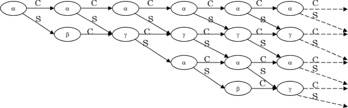
Data dependency in general systolic architecture
Fig. 3 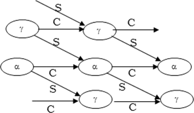
PEs of systolic architecture in two-dimensional array


This organization allows us to optimize the number of clock cycles. Each processing element in Fig. 11 is responsible for performing arithmetic operations. The different processing elements establish communication with the control block (FSM) as shown in Fig. 10 by receiving start signals at each state of Montgomery algorithm iteration. Each PE sends a done signal to the FSM at each end of the calculation. The final result is a concatenation of the last output of gamma and gamma_final PEs. The structure of all PEs has a combinational behaviour.
4.3 Internal Architectures of Cells
In this section, we will describe the internal architectures of PEs used in these designs. Our five cells are designed in order to use DSP(s) blocks.
Description of the Cell α
As illustrated in Fig. 4, the multiplication between a[i] and b[j] words returns a 2w bit result. This result is added thereafter to S_α_I n. This latter is the least significant bits of the result of processing element gamma, which is provided through the output multiplexer. The last add is also added to C_α_I n. The C_α_I n is the most significant bits of the result of the previous processing element alpha, which is provided also through an output of a second multiplexer. The different inputs/outputs of the PE alpha are presented in Fig. 10. The most significant bits of the result of alpha is propagated to the multiplexer to fix the next PE of alpha, whereas the least significant bits are propagated to the other multiplexer to fix the next PE of gamma. After each computation of the alpha PE, a shift in the input b is triggered.

Alpha processing element internal architecture
Description of the Cell β
According to our Algorithm 4 and as illustrated in Fig. 5, the zero index word of p (p[0]) and p ′ is provided to this beta processing element. The number p ′ corresponds the modular inverse of p modulo 2w. The multiplication between p ′ and S_β_I n returns a 2w bit result, where only the least significant bits of this multiplication is multiplied by the first word of p and returns a 2w bit result. Finally, this result is added to a w bit word S_β_I n. Only the most significant bit part of this result is used in the next gamma PE. The different inputs/outputs of PE beta are presented in Fig. 10.

Beta processing element internal architecture
Description of the Cell γ
As illustrated in Fig. 6, the multiplication between m and p[j] words returns a 2w bit result. This latter is added thereafter to S_γ_I n. The number S_γ_I n corresponds to the least significant bits of the result of processing element alpha, which is provided through an output multiplexer. This add is also added to C_γ_I n, where C_γ_I n is the most significant bits of the result of the previous processing element gamma. This PE gamma is provided also through an output of a second multiplexer. The different inputs/outputs of the gamma PE are shown in Fig. 10. The most significant bits of result are propagated to the multiplexer to fix the next PE of gamma, whereas the least significant bits are propagated to the other multiplexer to fix the next PE of alpha.

Gamma processing element internal architecture
Description of the Cell α f
The cell α f corresponds to the final α computed at the end of the line correspond to the multiplication step. In the PE alpha_final, the S_α_f_I n added to C_α_f returns a 2w bit result as presented in Fig. 7.

Alpha_f processing element internal architecture
Description of the Cell γ f
The cell γ f corresponds to the final γ computed at the end of the line correspond to the reduction step. For processing element gamma_final, S1_γ_f_I n is added to C_γ_f, the result is a 2w bit. The least significant bits of the last result is added to S2_γ_f_I n. The internal architecture of the gamma _final-type PE is presented in Fig. 8.

Gamma_f processing element internal architecture
In the remainder of this section, we detail our design for s = 8 and s = 16 architectures, respectively, denoted by NW-8 and NW-16.
4.4 Our Architectures
Firstly, we will start with the NW-8 architecture which contains three PEs of type alpha and three of type gamma. With this design, we can compute a modular multiplication in 33 clock cycles. Secondly, we will present the NW-16 architecture that is composed by six PEs of type alpha and six PEs of type gamma. And we can perform a modular multiplication with this architecture in 66 clock cycles. Similarly, in order to implement the NW-32 architecture and the NW-64 architecture, we need every time to double the number of cells. We provide a comparison of our architectures at the end of this section.
NW-8 Architecture
In this architecture, the operands and the modulo are divided in eight words as illustrated in Fig. 11. As illustrated in Fig. 9, the NW-8 architecture is composed of nine processing elements distributed in a two-dimensional array. Every processing element is responsible for the calculus involving w bit words of the input operands. For example, for a 256-bit modular multiplication with NW-8, the operands are split in eight words of 32 bits which results in a two-dimensional array of nine processing elements. The nine processing elements are divided in the following manner: three cells alpha, one cell alpha_final, one cell beta, three cells gamma and one cell gamma_final. Those choices were made in order to optimize the number of states in our FSM. As seen in Section 2, each PE in the N-dimensional array is connected to 2N data In/Out paths for communicating with 2N PEs in the N-dimensional array. Since we are working with two-dimensional elements, each

CIOS NW-8 architecture
PE in our design is connected to four data paths, two inputs and two outputs as presented in Fig. 3. In this architecture, the processing elements are designed with FSM. The control block communicates with the PEs and shift registers through start signals. The Fig. 10 presents an overview of our architecture. For more technical details, the Fig. 25 presents the different PEs with input/output. The shift register is designed to provide the required words for a modular multiplication to the PEs. The processing element alpha requires words a[i] and b[j] of the operands a and b; on the other side, the processing element gamma required a words of the operand p. Thus, these operands are defined in the package body. At the end of the Montgomery modular multiplication, the control block provides the multiplication result a ⋅ b ⋅ R − 1 mod p through the outputs of the last gamma and gamma_final processing elements. To evaluate the number of clock cycles for a CIOS method of modular multiplication in NW-8, the first parameter is max {number of alpha, number of gamma } = 3; it means that our design can handle three iterations of i at the same time as illustrated in Fig. 11. Implying that our algorithm requires to loop s + 3 times, we can perform our design in 33 clock cycles since our design requires three states (33 = 3 × (s + 3)). The different results of this architecture in bit-length 256 are given in Table 2. And we illustrate a part of the execution of this architecture in the Appendix B. To ensure the use of the word adapted to each step of execution, we used the rotations and shift. The operand B was divided into three vectors: the first vector is of size three words, the second vector is of size three words and the last vector is of size two words. Then, we need three rotations for this three vectors. Similarly, the modulo is divided into four vectors. And we used four rotations. Figure 12 illustrates the different rotations used in our architecture of NW-8.

Proposed Montgomery modular multiplication architecture

The data dependency graph of the proposed new systolic architecture with a two-dimensional array of processing elements (NW-8)

Internal architectures—rotations
NW-16 Architecture
In this architecture, the operands and the modulo are divided in 16 words as presented in Fig. 15. As illustrated in Fig. 13, the NW-16 architecture is designed in the same way as the NW-8. This example illustrates the scalability of our design. The NW-16 architecture is composed of 15 processing elements distributed in a two-dimensional array, where every processing element is responsible for the calculus involving w bit words of the input operands (Fig. 14). The 15 processing elements are divided like this: 6 cells alpha, 1 cell alpha_final, 1 cell beta, 6 cells gamma and 1 cell gamma_final. We can remark that the number of PEs of type alpha and gamma is the double of the number for NW-8. As said previously, the number of other PE type (alpha _final, beta, gamma _final) remains unchanged whatever the number of words in the design. We illustrate our architecture in Fig. 15. In order to evaluate the number of clock cycles of the NW-16 architecture, the first parameter is max {number of alpha, number of gamma } = 6, implying that our algorithm requires to loop s + 6 times. We can perform the multiplication with our design in 66 clock cycles since our design requires three states (66 = 3 × (s + 6)). The different results of this architecture in bit-length 256 are given in Table 3. In this version, the operand B was divided into six vectors, the first six vectors are of size three words, and the last vector is of size one word. Then, we need six rotations for this six vectors. Similarly, the modulo is divided into seven vectors. But we used five rotations.

CIOS NW-16 architecture

Proposed Montgomery modular multiplication architecture for the NW-16 version

The data dependency graph of the proposed new systolic architecture with a two-dimensional array of processing elements (NW-16).
NW-32 Architecture
In this architecture, the operands and the modulo are divided in 32 words. The NW-32 architecture is composed of 27 processing elements distributed in a two-dimensional array, where every processing element is responsible for the calculus involving w bit words of the input operands. The 27 processing elements are divided like this: 12 cells alpha, 1 cell alpha_final, 1 cell beta, 12 cells gamma and 1 cell gamma_final. In order to evaluate the number of clock cycles of the NW-32 architecture, the first parameter as we have seen previously is max {number of alpha, number of gamma } = 12, implying that our algorithm requires to loop s + 12 times. We can perform the multiplication with our design in 132 clock cycles since our design requires three states (132 = 3 × (s + 12)).
NW-64 Architecture
In this architecture, the operands and the modulo are divided in 64 words. The NW-64 architecture is composed of 51 processing elements distributed in a two-dimensional array, where every processing element is responsible for the calculus involving w bit words of the input operands. The 51 processing elements are divided like this: 24 cells alpha, 1 cell alpha_final, 1 cell beta, 24 cells gamma and 1 cell gamma_final. In order to evaluate the number of clock cycles of the NW-64 architecture, the first parameter is max {number of alpha, number of gamma } = 24, implying that our algorithm requires to loop s + 24 times. We can perform the multiplication with our design in 264 clock cycles since our design requires three states (264 = 3 × (s + 24)).
NW-s Architecture
In this subsection, we will generalize our design. With the same manner in the previous architectures, we can propose a generic version. The operands and the modulo are divided in s-words. The NW-s architecture is composed of nbc (number of cells) processing elements distributed in a two-dimensional array, where every processing element is responsible for the calculus involving w bit words of the input operands, where nbc = (s − s/4) + 3 cells (nbc is the number of cells). The number of clock cycles is 3 × (s + n b) with nb = max {number of cells alpha, number of cells gamma\(\}=\frac {(s-s/4)}{2}\), implying that our algorithm requires to loop s + n b times. We can perform the multiplication with our design in 3 × (s + n b) clock cycles since our design requires three states.
Architecture Comparison
Table 4 explains a comparison between the different architectures. The number of clock cycles for every architecture is equal to 3 × (s + nb), such that nb = max {number of cells alpha, number of cells gamma }, implying that our algorithm requires to loop s + n b times. It is interesting to notice that all our architectures are scalable and targeting the different security levels useful in cryptography.
5 Results
Table 5 summarizes the Field-Programmable Gate Array result postimplementation of the proposed versions of modular multiplication architectures. We present a results for both architectures NW-8 and NW-16. The designs were described in hardware description languages (VHDL) and synthesized for Artix-7 and Virtex-5 Xilinx Field-Programmable Gate Array’s. In order to check the correctness of the result, we compare the results given by the Field-Programmable Gate Array with the sage code. We present the different results after implementation of bit-length k which are given in Table 5. These circuits have the advantage of suitability to various applications with different bit lengths like RSA, ECC and pairings. As it is shown in Table 5, an interesting property of our design is the fact that the clock cycles are independent from the bit length. This property gives to our design the advantage of suitability to different security level. In order to implement the modular Montgomery multiplication for fixed security level, we must choose the most suitable architecture. Our architectures use the DSPs; the number of DSPs used depends on the number of cells and the number of iterations needed. The results presented in this work are compared with the previous work [4, 5, 17, 18] in Table 6. We could notice that our results are better than [18] considering every point of comparison, i.e. the number of slice and the number of clock cycles. Considering the number of slices, we recall that [18] used an external memory to optimize the number of slices used by their algorithms. Considering the comparison with [17], our design requires less number of slices and a better frequency and we really improve the number of clock cycles. Our design performed the Montgomery multiplication in 66 clock cycles for the 512 and 1024 bit length corresponding to AES-256 and AES-512 security level, while [17] performed the multiplication in 1540 clock cycles for the AES-256 security level and 3076 for the AES-512 security level.
About our general architecture, we have nbc = (s − s/4) + 3 cells to loop s + n b times. That allows to perform the multiplication in 3 × (s + n b) clock cycles.
6 Conclusion
In this paper, we have presented an efficient hardware implementation of the CIOS method of Montgomery multiplication algorithm over large prime characteristic finite fields \(\mathbb {F}_{p}\). We give the results of our design after routing and placement using a Artix-7 and Virtex-5 Xilinx Field-Programmable Gate Array’s. Our systolic implementations are suitable for every implementation, implying a modular multiplication, for example RSA, ECC and pairing-based cryptography. Our architectures and the designs were matched with features of the Field-Programmable Gate Array’s. The NW-8 design presented a good performance considering l a t e n c y × a r e a efficiency. This architecture can run for all the bit length corresponding to classical security levels (128, 256, 512 or 1024 bits) in just 33 clock cycles. On the other hand, the NW-16 performs the same bit length in 66 clock cycles, but improves in area compared to NW-8 work. Our systolic design using this method CIOS is scalable for other number of words.
References
Bigou K, Tisserand A (2015) Single base modular multiplication for efficient hardware RNS implementations of ECC. In: Conference on cryptographic hardware and embedded systems, pp 123–140
Fan J, Sakiyama K, Verbauwhede I (2007) Montgomery modular multiplication algorithm on multi-core systems. In: IEEE workshop on signal processing systems, 2007, pp 261–266
Hariri A, Reyhani-Masoleh A (2009) Bit-serial and bit-parallel Montgomery multiplication and squaring over GF. IEEE Trans Comput 58(10):1332–1345
Harris D, Krishnamurthy R, Anders M, Mathew S, Hsu S (2005) An improved unified scalable radix-2 Montgomery multiplier. In: 17th IEEE symposium on computer arithmetic, 2005. ARITH-17 2005, pp 172–178
Huang M, Gaj K, El-Ghazawi T (2011) New hardware architectures for Montgomery modular multiplication algorithm. IEEE Trans Comput 60(7):923–936
Huang M, Gaj K, Kwon S, El-Ghazawi T (2008) An optimized hardware architecture for the Montgomery multiplication algorithm. In: Cramer R (ed) Public key cryptography – PKC 2008, vol 4939 of lecture notes in computer science. Springer, Berlin, pp 214–228
Lee K -I (2007) Algorithm and VLSI architecture design for h.264/AVC Inter Frame Coding. PhD thesis, National Cheng Kung University, Tainan, Taiwan
Iwamura K, Matsumoto T, Imai H (1993) High-speed implementation methods for RSA scheme. In: Rueppel R A (ed) Advances in cryptology—EUROCRYPT’ 92, vol 658 of lecture notes in computer science. Springer, Berlin, pp 221–238
Iwamura K, Matsumoto T, Imai H (1993) Systolic-arrays for modular exponentiation using Montgomery method. In: Rueppel R A (ed) Advances in cryptology — EUROCRYPT’ 92, vol 658 of lecture notes in computer science. Springer, Berlin, pp 477–481
Joux A (2004) A one round protocol for tripartite Diffie-Hellman. J Cryptol 17(4):263–276
Koç C K, Acar T, Kaliski B S Jr (1996) Analyzing and comparing Montgomery multiplication algorithms. IEEE Micro 16(3):26–33
Koblitz N (1987) Elliptic curve cryptosystems. Math Comput 48(177):203–209
Manochehri K, Pourmozafari S, Sadeghiyan B (2010) Montgomery and RNS for RSA hardware implementation. Cpmput Inform 29:849–880
Kung H T (1982) Why systolic architectures? Computer 15(1):37–46
Miller V (1986) Use of elliptic curves in cryptography. In: Williams H C (ed) Advances in cryptology—CRYPTO ’85 proceedings, vol 218 of lecture notes in computer science. Springer, Berlin, pp 417–426
Montgomery P L (1985) Modular multiplication without trial division. Math Comput 44(170):519–521
Ors S B, Batina L, Preneel B, Vandewalle J (2003) Hardware implementation of a Montgomery modular multiplier in a systolic array
Perin G, Mesquita D G, Martins J B (2011) Montgomery modular multiplication on reconfigurable hardware: systolic versus multiplexed implementation. Int J Reconfig Comput 2011:61–610
Rivest R L, Shamir A, Adleman L (1978) A method for obtaining digital signatures and public-key cryptosystems. Commun ACM 21:120–126
Tenca A F, Koç Ç K (1999) A scalable architecture for Montgomery multiplication. In: Koç cCK, Paar C (eds) Cryptographic hardware and embedded systems, first international workshop, CHES’99, Worcester, MA, USA, August 12–13, 1999, Proceedings, vol 1717 of Lecture Notes in Computer Science. Springer, pp 94–108
Vucha M, Rajawat A (2011) Design and FPGA implementation of systolic array architecture for matrix multiplication. Int J Comput Appl 26(3):0975–8887
Author information
Authors and Affiliations
Corresponding author
Appendices
Appendix A
1.1 A.1 Code Sage NW-8

1.2 A.2 Code Sage NW-16

Appendix B: Architecture
1.1 B.1 Execution

Step 1

Step 2

Step 3

Step 4

Step 5

Step 6

Step 7

Step 8

Step 9

All processing elements
Rights and permissions
About this article

Cite this article
Mrabet, A., El-Mrabet, N., Lashermes, R. et al. A Scalable and Systolic Architectures of Montgomery Modular Multiplication for Public Key Cryptosystems Based on DSPs. J Hardw Syst Secur 1, 219–236 (2017). https://doi.org/10.1007/s41635-017-0018-x
Received:
Accepted:
Published:
Issue Date:
DOI: https://doi.org/10.1007/s41635-017-0018-x