
Abstract
In this paper, a new highly energy-efficient switching scheme is presented for successive approximation register analogue-to-digital converters. The proposed method applies a four-level switching strategy to reduce the switching energy to one of the lowest levels reported yet. Also, the controller of this method has low complexity compared to the other procedures. In contrast to the conventional scheme, the switching energy is reduced by 97.85% and the total capacitor size is decreased by 87.5%. Moreover, under the condition of the 50-times Monte-Carlo simulation for capacitor mismatch and reference voltages mismatch (Vref/2 and Vref/4), the mean value of the effective number of bit (ENOB) with standard deviation of 1% is 7.4 and 7.33 bits, respectively, while the ENOB value without any mismatches is 7.51 bits with sampling frequency of 1MS/s. It is noteworthy that the Monte-Carlo simulations are performed in Spectre simulator in Cadence with consideration all of non-idealities such as transistor charge injection, clock jitter and clock feedthrough. In other words, accurate and electrical simulation is performed instead of behavioral simulation. As a result, the bar graph of the ENOB values is plotted in MATLAB. In addition, the maximum and minimum of DNL/INL values are between − 0.3/0.3 LSB.
1 Introduction
Successive approximation register (SAR) analogue-to-digital converter is used in different applications, such as biomedical domain [6, 9, 12, 14, 16, 21, 23], wearable devices [3] and sensors [11, 24], due to low power consumption, low complexity, small area and straightforward structure. SAR ADC consists of digital-to-analogue converter (DAC), bootstrapped switches, comparator and SAR logics. SAR control logic includes shift register, shift code register and logic gates that controls how the capacitor arrays are switched. Also, The DAC section consists of capacitor arrays which are switched to special voltage levels for accurate conversion. That may result in significant switching energy drawn from the reference voltages during conversion. Recently, several techniques have been presented to reduce the switching energy of DACs and also the chip area [4, 5, 8, 10, 15, 17, 20, 22, 26]. The monotonic technique [10], Vcm-based method [26], tri-level switching scheme [22], Rahimi and Yavari approach [15], Xie et al. [20], Ghanavati [4], Sanyal and Sun [17], LSB split [5] and Vaq-based methods [8] reduce the switching energy of DAC by 81.26%, 87.52%, 96.89%, 93.7%, 96.91%, 97.67%, 98.4%, 99.2% and 96.48%, respectively, compared with the conventional method. The monotonic and Vcm-based methods reduce the chip area by 50% over the conventional scheme. All the tri-level scheme and switching methods in [15, 17, 20] achieve 75% area reduction. The area reduction by the Ghanavati, LSB split and Vaq-based techniques is 87.5%. In contrast to the conventional method, the proposed switching scheme reduces the chip area by 87.5% and improves the switching energy by 97.85%.
2 Proposed Four-Level Switching Method
Figure 1 shows a 10-bit analogue-to-digital converter that uses the proposed switching scheme. In this scheme, top-plate sampling method is used. During the sampling phase, the bottom plate of MSB capacitors is connected to Vref/4 (denoted by Vaq as in [8]) in both sides, while the bottom plate of remaining capacitors is connected to the ground. In the following, the generation of first to fourth bit of a 4-bit ADC is explained. The pattern of higher bits is the same as the fourth bit.

Proposed 10-bit differential SAR ADC structure
Figure 2 shows the proposed switching scheme for a 4-bit SAR analogue-to-digital converter. At first, the input is directly sampled on the top plate of capacitors. In this state, the bottom plate of MSB capacitors is connected to Vaq in both sides, while the bottom plate of remaining capacitors is connected to the ground. After turning off the sampling switches, the MSB bit is generated at the first comparison without consuming any switching energy. To generate MSB-1 bit, the bottom plate of the MSB capacitor in capacitor array which samples the higher voltage is connected to the ground, and simultaneously, the bottom plate of the same capacitor in the other capacitor array is connected to Vref. As a result, the differential input signal is compared with ± 0.5 Vref, and MSB-1 bit would be determined. Then to generate MSB-2 bit, if both MSB and MSB-1 are 1, the bottom plate of all capacitors in positive capacitor array is connected to Vaq. Also, the bottom plate of all capacitors except MSB in negative capacitor array is connected to Vref. In this state, the sampled differential input is compared with + 0.75 Vref. Similarly, if MSB = 1 and MSB-1 = 0, the bottom plate of all capacitors in positive array is connected to Vaq, with the difference that the negative capacitor array remains unchanged. Therefore, the sampled differential input voltage is compared with + 0.25 Vref and MSB-2 is obtained with no switching energy. If MSB = 0, the changes are the reverse for positive and negative capacitor array. Now, for obtaining fourth bit, if MSB-2 is 1, the bottom plate of MSB capacitor in capacitor array which samples the higher voltage is connected to the ground and the remaining capacitors are constant. But if MSB-2 is 0, it is connected to Vcm, where Vcm is half of the reference voltage Vref. For the next bits, the procedure is the same as the fourth bit and the changes are applied to the next capacitors of the MSB.

Proposed switching method of 4-bit SAR ADC
Figure 3 shows the successive approximation waveform of the proposed switching scheme. In 6-bit state, the proposed procedure deviates from Vcm by an average of 61/480 Vref. Also, the maximum common-mode variation is 1/4 Vref. Thus, the proposed procedure can mitigate the effect of common-mode voltage variation on the performance of comparator.

Waveform of the proposed switching scheme
3 Parasitic Influence Analysis
As shown in the following figures, parasitic capacitances of bottom plate and top plate of the unit capacitances are named Cpb and Cpt, respectively. Four states (according to 4-bit SAR ADC) are considered for the proposed switching scheme to explain the effect of these capacitances on the DAC operation and consequently SAR converter.
-
1.
In the first state, as shown in Fig. 4, the voltage of C1 is set from Vaq to Vref. It can be calculated that the change in potential at point A is VA2 − VA1. As a result, the gain in presence of parasitic capacitances is calculated. Therefore,
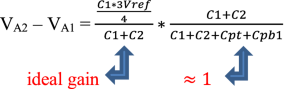 (1)
(1)Fig. 4 
The first state of parasitic capacitances effect calculation
-
2.
In the second state, as shown in Fig. 5, the voltage of C1 is set from Vaq to the ground:
 (2)
(2)Fig. 5 
The second state of parasitic capacitances effect calculation
-
3.
In the third state, as shown in Fig. 6, the voltage of C1 is set from Vaq to Vcm:
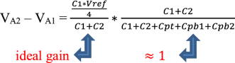 (3)
(3)Fig. 6 
The third state of parasitic capacitances effect calculation
-
4.
In the fourth state, as shown in Fig. 7, the voltage C1 is set from Vaq to the ground in other condition:
 (4)
(4)Fig. 7 
The fourth state of parasitic capacitances effect calculation


In a typical 0.13 µm process technology, the smallest unit capacitance is 17 fF, and the typical Cpb and Cpt are less than 1 fF [1, 25]. So we can conclude that the obtained gains in (1) to (4) are close to the ideal value. Also, similar to the analysis in paper [13], there are the same errors of parasitic capacitances in the high and low bits cycles. In conclusion, the parasitic capacitances do not affect the linearity of the proposed structure.
4 Dynamic Two-Stage Latched Comparator
Dynamic two-stage latched comparator is used for the proposed SAR ADC simulations. This comparator is energy efficient and fast and has low input referred offset voltage. The circuit of the two-stage comparator is illustrated in Fig. 8.

Two-stage comparator schematic [18]
The first stage is a voltage amplifier, and the second stage is a latch. During the reset phase when clock signal is low, PMOS transistors in the first stage (3 and 4) charge F nodes to VDD and turn off the latch stage. In this phase, the output nodes are reset to zero through NMOS switches (11 and 12) in the latch stage. This architecture is power efficient and fast due to low capacitance at F nodes which are mainly drain diffusion capacitances of NMOS and PMOS transistors connected to these nodes.
When clock turns to high in regeneration phase, the tail transistor is turned on and amplification in the first stage is initiated. F nodes start to discharge through differential input pair transistors (1 and 2) in the first stage. These nodes are discharged with different rates proportional to the input voltage. Once either of the output nodes of the first stage (F nodes) drops to an amount around Vth of the input transistors of the latch stage, these transistors (5 and 6) are switched on and the second stage is activated. Gradually, the output voltage increases and positive feedback system is activated and generates output level of high and low voltage in the regeneration phase.
The first stage consumes power only when the parasitic capacitances at F nodes are discharged. The second stage dissipates power until the rail-to-rail output voltage is generated. In this comparator, two inverters are added to recover the voltage level at the output of the comparator. A NAND-type SR latch is also used to hold the comparator result during the reset phase. NAND-type SR latch is shown in Fig. 9 [18].

NAND-type SR latch [18]
5 DAC Control Logic Analysis
A 4-bit SAR ADC which is introduced in Sect. 2 is used to investigate the DAC control logic. DAC control logic of the proposed switching scheme is shown in Fig. 10. This controller has low complexity compared with the other schemes. Also, as the process technology improves, the total power consumption in SAR control logic becomes small enough. A comparison of logic complexity between the proposed method and the previous procedures is shown in Table 1.

Control logics of the proposed switching method for 4-bit state
6 Switching Energy and Comparison
The behavioral simulation of the proposed switching scheme and the switching method reported in [8] for 10-bit ADC was performed by MATLAB software, and the results are shown in Fig. 11. In addition, the average switching energy and the total DAC capacitor for different switching schemes are compared in Table 1. The proposed switching method consumes only 29.3CVref2 average switching energy which results in a reduction of 97.85% over the conventional scheme. Moreover, the same as [4, 5, 8] the proposed scheme employs 256 unit capacitors and thus achieves 87.5% reduction in the total DAC capacitor compared with the conventional one. Also, the chip area is optimized by 50% in comparison with the published schemes in [15, 17, 20, 22]. The proposed switching method consumes 39% less energy compared to the switching scheme in [8].

Switching energy at each output code
7 Simulation Results
In this section, the proposed 8-bit SAR ADC is simulated in 0.13 µm CMOS process technology with sampling frequency of 1MS/s and supply voltage of 1.2 V. Consequently, power consumption, dynamic and static parameters are calculated. Also, 50-times Monte-Carlo simulation is performed for capacitor mismatch and reference voltages mismatch separately.
7.1 Fast Fourier Transform (FFT)
The dynamic performance is evaluated by calculating the SFDR, SINAD(SNDR) and ENOB of ADC. For this purpose, a full swing sinusoidal wave with fin = 22.46 kHz, which is based on coherent sampling, is applied to the input of ADC. The simulation is performed to achieve 1024 samples with sampling frequency of 1 ms/s. Then, fast Fourier transform of the stored output data is executed in MATLAB, and by performing some post-processing, the SFDR, SINAD and ENOB are measured.
The FFT of 8-bit ADC output voltage is shown in Fig. 12. The simulation results demonstrate that the ADC has SINAD = 46.96 dB, SFDR = 56.92 dB and achieves 7.51 bits of ENOB which all exhibit a good performance of proposed ADC in terms of linearity and noise characteristics.

FFT of the ADC output for Fin = 22.46 kHz
Energy per conversion-step can be calculated using FOM definition of ADC which is given by Eq. 5 [4].

Table 2 summarizes the performance parameters of the proposed SAR ADC.
Also, a separate simulation is performed in frequency of 497.07 kHz (Nyquist rate) and the dynamic parameters are measured. As a result, SINAD, SFDR, SNR, ENOB and FOM are achieved 47.12 dB, 57.36 dB, 49 dB, 7.54 bits and 62.11 fJ/conversion-step, respectively. Therefore, the FFT of 8-bit ADC output voltage with new requirements is shown in Fig. 13. Also, Table. 3 summarizes the performance parameters of the proposed SAR ADC. The achieved results show that there is no large difference between Nyquist rate and the used oversampling rate. In fact, the proposed SAR ADC has a good performance in both of the frequency rates. In addition, Fig. 14 shows the ENOB of proposed ADC with respect to the input frequency, where the ENOB remains almost constant over the entire bandwidth. Hence, the effective resolution bandwidth (ERBW) is higher than the Nyquist bandwidth.

FFT of the ADC output for Fin = 497.07 kHz (Nyquist rate)

ENOB of the ADC versus input frequency
7.2 DNL/INL and Offset Evaluation
Input/output transfer curve is helpful to obtain the static errors such as DNL/INL and offset. A differential ramp signal from 0 to 1.6 Vp–p is applied to ADC in steps of LSB/4. The stored data are executed in MATLAB, and, as a result, the DNL/INL and offset are calculated. Figure 15 shows a part of the input/output transfer curve.

Actual ADC transfer curve
Figures 16 and 17 show the DNL and INL plots, respectively. In these figures, it can be seen that the maximum and minimum of DNL/INL are + 0.26/− 0.24 LSB and + 0.26/− 0.28 LSB, respectively. There is no missing code because none of the DNL errors are less than − 1 LSB or more than + 1 LSB. The offset error is + 1 LSB. The major contribution of DNL and INL errors can be attributed to the charge injection of the switches, quantization noise and the limited number of samples taken per code.

DNL plot

INL plot
7.3 Power Consumption
The distribution of power consumption between different blocks of ADC is shown in Fig. 18. Shift register and shift code register consume the largest amount of power among other blocks which is 57%. After them, logic gates with 33.84%, comparator with 5.27% and DAC with 3.89% consume the largest amount of power, respectively. In order to decrease the leakage power even more, and simultaneously maintaining the speed, the combination of high and low threshold voltage transistors for some parts of ADC can be used. Also, the use of new process technology, lower supply voltages and transistors with lower dimension can be helpful. It can be noted that the unit capacitance value in this simulation is 20 fF.

Pie chart of power distribution
7.4 Monte-Carlo Simulation
Unlike some previously reported works [19, 27] in which the Monte-Carlo simulation is performed on behavioral model of circuit in MATLAB, the Monte-Carlo simulation in this paper is performed in Spectre simulator on electrical model of circuit. By this way, the effect of all non-idealities such as transistor charge injection, clock jitter and clock feedthrough are taken into account. In the electrical model of the proposed SAR ADC, a Gaussian random variable with standard deviation of 1% is added to the value of the unit capacitor. As shown in Fig. 19, according to Monte-Carlo simulation with 50 runs and by applying errors on the capacitors' value, the mean value of ENOB would be 7.4 bits. Also, the Monte-Carlo simulation result of ENOB for the case that the random errors are applied to the voltages of Vaq and Vcm is given in Fig. 20. Accordingly, the mean value of ENOB would be 7.33 bits as a result of mismatch in Vaq and Vcm.

50-Times Monte-Carlo capacitor mismatch simulation

50-Times Monte-Carlo simulation for Vaq and Vcm mismatch
8 Conclusion
In this paper, a new energy-efficient four-level switching scheme is presented. In this method, in addition to the previous reference voltages, the Vaq voltage is used, which is a quarter of the reference voltage Vref. The proposed switching scheme has one of the highest amounts of energy saving among other methods and consumes only 29.3CVref2 average switching energy. Moreover, because of using reference voltage Vaq, the number of unit capacitors decreases to 256. Therefore, ADC chip area decreases by 87.5% compared with the conventional scheme. In addition, the complexity of the controller of this scheme is relatively low and also the proposed method is less sensitive to the parasitic capacitances. Moreover, Monte-Carlo simulations on electrical model of the proposed ADC demonstrate that the mean value of ENOB against capacitor mismatch and reference voltages mismatch is close to ideal value (when no mismatch exists) and their standard deviations from the mean are 0.11 and 0.22 bits, respectively.
References
S. Brenna, A.G. Bonfanti, A. Abba, F. Caponio, A.L. Lacaita, Analysis and optimization of a SAR ADC with attenuation capacitor, in 37th International Convention on Information and Communication Technology, Electronics and Microelectronics (MIPRO) (2014)
Y.S. Chen, Y.Q. Zhuang, H.L. Tang, A 99.8% energy-reduced two-stage mixed switching scheme for SAR ADC without reset energy. Circuits Syst. Signal Process. 38, 5426–5447 (2019)
W. Gao, S. Emaminejad, H.Y.Y. Nyein, S. Challa, K. Chen, A. Peck, H.M. Fahad, H. Ota, H. Shiraki, D. Kiriya, Fully integrated wearable sensor arrays for multiplexed in situ perspiration analysis. Nature 529, 509–514 (2016)
B. Ghanavati, E. Abiri, A. Keyhani, M.R. Salehi, A. Sanyal, An energy efficient SAR ADC with lowest total switching energy consumption. Analog Integr. Circuits Signal Process. 97, 123–133 (2018)
B. Ghanavati, E. Abiri, M.R. Salehi, A. Keyhani, A. Sanyal, LSB split capacitor SAR ADC with 99.2% switching energy reduction. Analog Integr. Circuits Signal Process. 93, 375–382 (2017)
W. Guo, Z. Zhu, A 0.3 V 8-bit 8.9 fJ/con.-step SAR ADC with sub-DAC merged switching for biosensors. Microelectron. J. 68, 44–54 (2017)
L. Jian, R.X. Ding, S.B. Liu, Z.M. Zhu, A highly energy-efficient, highly area-efficient capacitance multiplexing switching scheme for SAR ADC. Analog Integr. Circuits Signal Process. 96, 207–215 (2018)
Z. Jinqiang, M. Niansong, Z. Zhaofeng, M. Lingqin, Vaq-based tri-level switching scheme for SAR ADC. Electron. Lett. 54, 66–68 (2018)
T. Kim, S. Kim, A 12.1 mW, 60 dB SNR, 8-channel beamforming embedded SAR ADC for ultrasound imaging systems, in IEEE Asian Solid-State Circuits Conference (A-SSCC) (2017), pp. 141–144
C.C. Liu, S.J. Chang, G.Y. Huang, Y.Z. Lin, A 10-bit 50-MS/s SAR ADC with a monotonic capacitor switching procedure. J. Solid State Circuits 45, 731–740 (2010)
S. Liu, Y. Shen, J. Wang, Z. Zhu, A 10-bit self-clocked SAR ADC with enhanced energy efficiency for multi-sensor applications. IEEE Sens. J. 10, 4223–4233 (2018)
D.J. Moni, S.M. Jose, Design of 10b SAR ADC for biomedical applications, in International Conference on Electronics and Communication Systems (ICECS) (2015), pp. 276–281
D. Osipov, S. Paul, Two-step reset method for energy-efficient SAR ADC switching schemes. Electron. Lett. 52, 816–817 (2016)
C.S. Ragit, S. Badjate, Design of up-down counter as SAR logic for high speed SAR ADC used in health care system, in Conference on Advances in Signal Processing (CASP) (2016), pp. 465–468
E. Rahimi, M. Yavari, Low-efficient high-accuracy switching method for SAR ADCs. Electron. Lett. 50, 499–501 (2014)
S. Ur Rehman, A.M. Kamboh, A CMOS micro-power and area efficient neural recording and stimulation front-end for biomedical applications. Circuits Syst. Signal Process. 34, 1725–1746 (2015)
A. Sanyal, N. Sun, SAR ADC architecture with 98% reduction in switching energy over conventional scheme. Electron. Lett. 49, 248–250 (2013)
E.V. Tuijl, P. Geraedts, D. Schinkel, E. Klumperink, B. Nauta, M. Van Elzakker, A 1.9 μW 4.4 fJ/Conversion-step 10b 1 ms/s Charge-Redistribution ADC. ISSCC Dig. Tech. Papers (2008)
W.L. Wu, S.W. Sin, U. Seng-Pan, R.P. Martins, A 10-bit SAR ADC with two redundant decisions and splitted-MSB-cap DAC array, in IEEE Asia Pacific Conference on Circuits and Systems (2012), pp. 268–271
L. Xie, J. Su, J. Liu, G. Wen, Energy-efficient capacitor-splitting DAC scheme with high accuracy for SAR ADC. Electron. Lett. 51, 460–462 (2015)
K. Yadav, P. Patra, A. Dutta, A 43-nW 10-bit 1 ks/s SAR ADC in 180 nm CMOS for biomedical applications, in IEEE Asia Pacific Conference on Postgraduate Research in Microelectronics and Electronics (PrimeAsia) (2015), pp. 21–25
C. Yuan, Y. Lam, Low-energy and area-efficient tri-level switching scheme for SAR ADC. Electron. Lett. 48, 482–483 (2012)
Y. Zhang, Y. Li, Z. Zhu, A charge-sharing switching scheme for SAR ADCs in biomedical applications. Microelectron. J. 75, 128–136 (2018)
X. Zhong, B. Zhang, A. Bermak, C.Y. Tsui, M.K. Law, A low-power compression-based CMOS image sensor with microshift-guided SAR ADC, in IEEE Transactions on Circuits and Systems II Exp. Briefs, vol. 65, pp. 1350–1354 (2018)
R. Zhou, S. Liu, J. Liu, R. Ding, J. Wang, S. Huang, Z. Zhu, A 96.88% area-saving and 99.72% energy-reduction switching scheme for SAR ADC with a novel two-step quantisation technique. Analog Integr. Circuits Signal Process. 100, 205–213 (2019)
Y. Zhu, C.H. Chan, U.F. Chio, S.W. Sin, R.P. Martins, F. Maloberti, U. Seng-Pan, A 10-bit 100-MS/s reference-free SAR ADC in 90 nm CMOS. J. Solid State Circuits 45, 1111–1121 (2010)
Y. Zhu, U.F. Chio, H.G. Wei, S.W. Sin, S.P. U, R.P. Martins, Linearity analysis on a series-split capacitor array for high-speed SAR ADCs. in 51th Midwest Symposium on Circuits and Systems, pp. 922–925 (2008)
Author information
Authors and Affiliations
Corresponding author
Additional information
Publisher's Note
Springer Nature remains neutral with regard to jurisdictional claims in published maps and institutional affiliations.
Rights and permissions
About this article

Cite this article
Sotoudeh, M., Rezaei, F. A Four-Level Switching Scheme for SAR ADCs with 87.5% Area Saving and 97.85% Energy-Reduction. Circuits Syst Signal Process 39, 4792–4809 (2020). https://doi.org/10.1007/s00034-020-01405-x
Received:
Revised:
Accepted:
Published:
Issue Date:
DOI: https://doi.org/10.1007/s00034-020-01405-x