
Abstract
In today’s technology, optical networking plays a vital role in reducing data losses, thereby providing higher data rates between the transreceivers. The very large scale integration circuits in the modulator–demodulator (MODEM) usually fabricated using complementary metal oxide semiconductor (CMOS) technology have serious scaling limitations; hence, device scaling beyond 65 nm technology becomes highly challenging. Quantum-dot cellular automata (QCA) is one of the most promising nanotechnologies that enable areas of smaller size, i.e. 60% less design area than the CMOS technology, with capability to produce high speed by taking less cycles compared with the other CMOS designs to reduce scaling issues. The QCA-based designs are considered as the best alternative solutions to the transistor-based (CMOS) designs. This paper deals with the implementation of the logic gates NOT, AND, OR, NAND, NOR, XOR and XNOR using both CMOS and QCA technologies, while the QCA allows more possible design structures for each logic gate to enable optimization of the area. Finally, the proposed QCA-based logic gate design and CMOS-based designs are compared in terms of the design area, cell count and the speed of the designs. QCA designer 2.0.3 and virtuoso CADENCE Computer-Aided Design tools are used for carrying out the work.
1 Introduction
In general, optical networking circuits are purely CMOS analog circuits. The major drawback with analog CMOS circuits is more silicon area occupied, low data rates due to more power dissipation, and the delay in the conversion process of electrical to optical and optical to electrical. Hence, these two blocks are needed for replacement with QCA to meet all the above shortcomings as shown in Fig. 1.

Synchronized optical networking block diagram
The density of IC and performance is growing rapidly with CMOS technology during the past few decades. However, CMOS–VLSI circuit designs are facing new challenges, such as short channel effects (SCEs) and test complexity at nanometre scale [13]. The International Technology Roadmap for Semiconductors (ITRS) has proposed a number of alternative nanoelectronic technologies, such as resonant tunnelling diodes (RTD), quantum-dot cellular automata (QCA) and single-electron transistor (SET), for dealing with the drawbacks seen in CMOS technology and for replacement of the transistor-based technology in the near future [2]. The QCA is the technology best suited for applications with the requirements of ultra-low power, ultra-dense and high operating frequencies (at THz), where the conventional CMOS devices can replace the QCA cells [1, 6, 16].
Section 2 of this paper explains the basics of QCA. The implementation procedure of QCA-based digital logic gates is outlined in Sect. 3. A comparative analysis of QCA-based logic gates designs made with the CMOS-based designs in terms of the design area, and the number of cells and the speed of the designs are discussed in Sect. 4. Section 5 provides the conclusion indicating the results achieved using the QCA technology.
2 Quantum-Dot Cellular Automata
The fundamental component in QCA technology is the QCA cell, which comprises four quantum dots situated one in each corner of the QCA cell. These quantum dots are connected through electron tunnel junctions. The QCA cell is in the form of a square of size 18 nm × 18 nm. Quantum dot is a single-electron-charge container with a size of 5 nm diameter [5]. The QCA cell with unpolarized state is shown in Fig. 2a, b. Depending on the orientation of electrons, the cell exhibits two polarizations P = − 1(logic 0) and P = + 1(logic 1), which are shown in Fig. 2c [4, 19, 22, 24].

a QCA cell anatomy; b elements in potential well; c cell polarization = − 1(logic ‘0’)
Each QCA cell has two electrons, which are positioned in two quantum dots in such a way that they always tend to occupy quantum dots that are located at the corners of the cell keeping maximum distance between them as a result of the columbic repulsion force between each other. The two electrons can quantum tunnel between the quantum dots mechanically, but they cannot tunnel between cells. They never travel beyond the QCA cell boundary and are restricted to stay within the same cell [9]. Once the polarization value is set, tunnelling effect occurs between the adjacent cells, and then the signal in turn propagates from one location to another. These cells are also called 90°cells.
Logical Elements in QCA Most fundamental building blocks (logical element) in the QCA technology for the implementation of any logic function are majority voter, inverter gate, wires and clock [23].
-
i.
Majority Voter A majority gate is made with five QCA cells arranged in the form of a cross as shown in Fig. 3a. Hence, the input state either logic ‘0’ or logic ‘1’ irrespective of the majority becomes the state of the output cell. The majority gate is an important element for the realization of any logic function.
Fig. 3 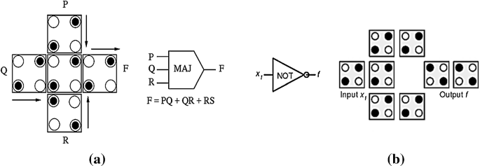
a Basic QCA majority gate function. b Majority gate truth table and corner form of NOT gate

For example, if inputs P and Q are in a binary ‘0’ state and input R is in a binary ‘1’ state, the majority gate output will be in a binary ‘0’ state. This is the result of the combined electrical field effect which is due to identical inputs of P and Q collectively greater than the input R which is kept at different inputs [17, 25]. The three-input majority gate outputs can be expressed in the Boolean form as shown in Eq. (1). The output for different input combinations is shown in Table 1.
-
ii.
NOT Function The NOT gate or inverter is a logic gate which has been used to implement a logical negation function. The basic NOT gate symbol and two different QCA-based NOT gate structures are shown in Fig. 3b. The arrangement of the cells in NOT gate QCA layout takes the benefit of geometry of cell adjustments [13]. A single QCA wire is bifurcated to two wires: that is, the output cell is situated adjacent to the bifurcated to ensure only the corners touch. This leads to the right of the bifurcated wire and the cells at the end of the bifurcated wire having the same adjustments. In addition, the cell on the right of the bifurcated wire does not adjust with electrons close to an electron at the corners and at the end of the bifurcated wire. Therefore, the adjustment at the right of the bifurcated wire gets inverted. The adjustments of the output cell at the right of the bifurcation are inversely proportional to the polarization of the cells at the end of the bifurcated wire indicating the output as always complementary to the input [20].
-
iii.
QCA Wires The connecting wire parameters are very crucial in the delay and loss of the data. A simple binary wire formed by the QCA cells using identical polarization [21] to propagate either logic ‘0’ or logic ‘1’ is presented in Fig. 4a. As shown in Fig. 4b angles are avoided in layout design of an inverter chain when drawing metal lines. The same QCA cell can be used for both the construction of the digital circuits and joining two different blocks together [10].
Fig. 4 
QCA wires: a using 90° chains of QCA cells; b 45° inverted chain of QCA cells

A simple binary wire in which the polarization of any of the cells in the arrangement requires a change by a ‘driver cell’, and then the rest of the cells would immediately synchronize to the new polarization value due to the columbic force between them. In this manner, a QCA wire can transmit the polarization state, namely either logic ‘0’ or logic ‘1’.
-
iv.
QCA Clocking Scheme Clock is the heart for any digital circuit. Circuit performance is strongly dependent on the clock. In QCA technology, the clock has two important functions, namely powering and getting synchronization. The synchronization between the circuits (controlling data flow) is necessary to define the direction of the cells. One QCA clock cycle contains four clock zones referred to as clock 0, clock 1, clock 2 and clock 3, respectively. The phase lag between the two successive clock phases is 90°, while the phase lag between the non-adjacent clock zones is 1800. The four clock phases or zones are switch, hold, release and relax as shown in Fig. 5, and each phase experiences a 90° phase delay [15].
Fig. 5 
Four-phase clocking of QCA

In the Switch phase, the cell is unpolarized to start with and inter-dot potential barriers are kept low. The inter-dot potential barriers are then slowly raised in accordance with the state of neighbouring (input) cell. This is the state during which an actual computation is performed. In the hold phase, the potential barriers are held so high so that any cell can serve as the input to the next stage. In the release phase, the potential barriers are lowered, and the cells are relaxed to get into unpolarized state. Finally, the cells are in a relaxed state with the potential barriers low and remain unpolarized. Controlling of the potential barriers between the adjacent quantum dots can be achieved by clocking of QCA [17].
3 Implementation of Basic Logic Gates
Any digital circuit contains logic gates in a large number. In logic gate design, area and speed of the circuit has been considered as a significant component in designing low power circuits. NOT, AND, OR, NAND, NOR, XOR and XNOR gates are implemented using CMOS technology which does not optimize the area due to its scaling limitations. Hence, all the logic gates are implemented through use of QCA technology, and the QCA layout allows optimization of the designs in the area, number of cells and increasing speed of both the combinational and sequential circuits.
-
i.
AND Gate AND logic is the basic logic, which produces high output only when all the inputs are high. With a slight modification to the majority voter function block, a two-input Boolean AND gate [18] function can be realized. The symbol of AND gate along with its QCA layout is shown in Fig. 6a, and the layout is shown in Fig. 6b. The AND function can be realized by fixing any one of the input cell of the majority gate to the fixed polarization of ‘− 1’. The output is shown in Eq. (2) [14].
Fig. 6 
a AND gate b AND gate layout

Both the inputs when held at logic ‘1’ sum up to a stronger Coulomb force than the single fixed ‘0’ cell, and hence, a majority gate output becomes logic ‘1’; otherwise, it is logic ‘0’. A simple one clock zone is enough for driving this gate and completing its operation. CMOS design requires 6 transistors for the two-input AND logic implementation. However, the QCA requires only 5 cells. Hence, 98% design area can be improved relative to the CMOS technology.
-
ii.
OR Gate Another basic logic function in the digital circuit is the OR logic. The OR gate majority voter logic symbol and QCA layout are presented in Fig. 7a. The CMOS logic layout is shown in Fig. 7b [20]. Fixing one input of the majority gate to logic ‘1’ helps its performance as logic OR function. Its output logic expression is shown in Eq. (3).
Fig. 7 
a Majority gate as OR gate b OR gate layout

When either of the inputs is at logic ‘1’, along with fixed ‘1’ cell it sums up to a stronger Coulomb force than the OR gate outputs logic ‘1’. Otherwise, the output is logic ‘0’ according to the function of the majority gate. The QCA-based design requires only 5 cells, whereas CMOS requires 6 transistors. Hence, the optimization in QCA is 98%. It needs only one clock zone for its operation, thereby improving the speed.
-
iii.
NOT Gate NOT gate is the basic logic function in any digital circuit in the implementation of the other logic functions. Inverter in combination with the majority gate either AND or OR gate can implement various logical functions, such as NAND and NOR, etc. [10]. NOT gate symbol is shown in Fig. 8a, and various possible QCA-based layouts of the NOT gate structures are presented in Fig. 8b, (i)–(iv). The logic expression for the output is shown in Eq. (4).
Fig. 8 
a NOT gate b (i), (ii), (iii) and (iv) NOT gate layout

There are 4 possible QCA layouts for the NOT function, where the first design takes less area than the other 3 designs. QCA-based design enables an improvement of 99.97% in design area over the CMOS design. In addition, each of four designs requires only one clock zone for its operation.
-
iv.
NOR Gate NOR is the universal logic function which facilitates implementation of any logic function. Generally, NOR gate is an OR gate followed by an inverter. The basic symbol of NOR gate is shown in Fig. 9a. The two different polarizations (NOR and TNOR) [22] possible in the QCA-based layout designs are shown in Fig. 9b (i) and (ii). The Boolean expression for the output of the NOR gate is given by Eq. (5)
Fig. 9 
a NOR gate layout b (i) and (ii) NOR gate layout

When both inputs A and B are at logic ‘0’, the OR gate produces logic ‘0’ as the output, but, as the NOT gate is connected at the output of OR along, its output is logic ‘1’. Otherwise, the output is logic ‘0’. The QCA NOR design takes 7 cells, and QCA-based TNOR design takes 5 cells, whereas CMOS requires 4 transistors, since the transistor size is far below the QCA cell and still with a 95% area optimization. The speed in QCA is high as both the structures require only one clock zone for performing its intended function.
-
v.
XOR Gate Another important logic in the digital circuits is the XOR logic. This is widely used in the adders, multipliers, comparators, multiplexer circuit, etc. The XOR logic symbol is shown in Fig. 10a. It acts as an odd detector in many applications. The authors have proposed F-shaped design, which is compared with XOR structures presented in Ref. [26], and the layouts are presented in Fig. 10b, i and (ii). They do not follow any Boolean function, but take advantage of the inherent characteristics of QCA cells to form XOR gate. The output of XOR gate is given by Eq. (6)
Fig. 10 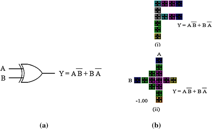
a XOR gates b (i) and (ii) XOR gate layout

Both the XOR designs are area efficient and optimized in comparison with the earlier XOR designs in QCA and CMOS designs. The F-shaped XOR structure needs 5 clock zones, and the latter needs only 2 clock zones for its operation. Hence, the second design is better in both area and speed. The QCA-based designs provide an improvement of 99.97% in the design area with respect to CMOS design.
-
vi.
XNOR Gate Another important logic block in the digital circuits is the XNOR. The basic XNOR logic symbol is presented in Fig. 11b. When even number of input is high, XNOR produces a high output; otherwise, the output provided is low [11]. This gate acts as an equality detector in many applications. The output Boolean expression for the two-input XNOR gate is given in Eq. (7).
Fig. 11 
a XNOR gate b (i) and (ii) XNOR gate layouts

The authors have proposed two different possible XNOR structures: shown in Fig. 11a cascaded with an inverter to form the XNOR layout as shown in Fig. 11b (i). If the polarization of the cell is altered from − 1 to + 1, the XOR function as XNOR is shown in Fig. 11b (ii). Both the designs are area efficient and speedy relative to the previous XNOR designs presented in Refs. [7, 12]. Both these designs take two clock zones for performing their functions.
The layouts in design-1 take 15 QCA cells, and design-2 take 14 cells; the counts in CMOS are 8 and 12, respectively. Hence, there is an improvement of 99% in the design area relative to that of the CMOS design.
-
vii.
Three-Input XOR Gate Three-input XOR gates have been presented with the help of the inherent characteristics of QCA cells to form an area-efficient and optimized XOR gate with a minimum delay relative to that of the existing structures presented in Fig. 12(a) [2]. The layout of three-input XOR is shown in Fig. 12(b). The output logic equation of the three-input XOR gate is given in Eq. (8).
Fig. 12 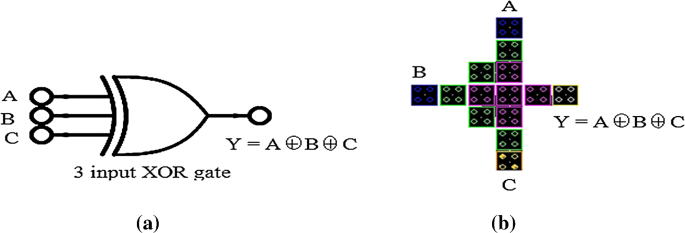
a Three-input XOR gate b layout of three-input XOR gate

It requires only two clock zones to perform the anticipated operation.
The authors have designed three-input XOR gates using QCA, which uses cells of a smaller number (cell count = 14) relative to the design in Ref. [3] (cell count = 16), whereas CMOS design requires 21 transistors. Hence, the design proposed by the authors is more area efficient than any other QCA design or CMOS designs.
-
viii.
NAND Gate NAND is another universal logic function, which can help implementation of any logic function. AND gate followed by an inverter is the NAND. The basic symbol of NAND gate is shown in Fig. 13a. Two different polarizations (NAND and TNAND) have been used in this paper to design different NAND gates based on the QCA, and layouts of the designs are presented in Fig. 13b (i) and (ii). The Boolean expression for the output of the NAND gate is given by AND gate output followed by an inverter as shown in Eq. (9)
Fig. 13 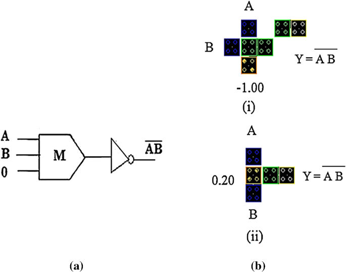
a NAND gate b (i) and (ii) NAND gate layout

The proposed design uses 5 QCA cells, which are less in count when compared with the designs in Refs. [8, 26], where the count is 7. CMOS design takes 4 transistors; the authors designs are more area efficient, i.e. 99% compared to the CMOS. Both the NAND gates use only one clock to complete its operation.
4 CMOS and QCA Technologies Comparison Results
In this paper, the proposed logic gates using QCA technology have been discussed and comparisons have been made with CMOS designs, as well as with the existing QCA designs in terms of design area, cell count and latency.
-
i.
Design Area of Logic Gates The logic gates proposed in this paper have been based on the QCA technology
Along with the design area utilized by each design in both QCA and CMOS technologies. Table 2 shows the design area of the gates in both CMOS and QCA technologies along reduces the area overhead related to the CMOS designs. Figure 14 shows the design area comparisons.

Design area of both CMOS and QCA designs graph
The graph showed the design area of the proposed NOT gate taking a smaller area which is equal to 0.0031 μm2 in QCA (in CMOS 12.15 μm2) when compared with the other existing NOT gates. Similarly, the proposed XOR design has a minimum area of 0.0092 μm2, and the existing design has 0.017 μm2. The proposed XNOR design area is 0.0092 μm2, which is smaller, compared to the existing design area of 0.019 μm2. The three-input XORs are required in the case of CMOS technology, whereas in the case of QCA technology, NOT gate requires a smaller area of 0.0031 μm2. In the graphical representation, QCA designs take a smaller area when compared with CMOS; it is not included in the graph.
-
ii.
Cell Count of Different Logic Gates Table 3 shows the number of transistors required by each design in CMOS technology and the number of cells required for QCA technology, additionally, shown as bar diagrams in Fig. 15.
Table 3 Transistors and cell count for logic gates comparison Fig. 15 
Cell/transistors count of both CMOS and QCA designs graph

From the graph, it is observed that the CMOS technology requires more transistors; the number of transistors required for most of the gates is higher than the cell count in QCA, i.e. one transistor = 45 nm2 and one QCA cell = 18 nm2. Hence, the less static power is consumed in case of the QCA; therefore, the data loss is minimum in this technology.
-
iii.
All Design Parameters for Logic Gates in QCA and CMOS Comparisons are made between all the proposed basic gates and universal gates in QCA with CMOS 45 nm technology designs in terms of area clock zones. The number of cells is listed in Table 4 and Fig. 16.
Table 4 Comparison of all parameters for both CMOS and QCA technology designs Fig. 16 
Overall design comparisons of both CMOS and QCA

The graph indicates the QCA-based designs as more area efficient than the CMOS. Hence, these are better suited for portable designs. In addition, the QCA-based designs take less cock zones and they are the best for high-speed applications. Finally, as the QCA takes less cell count, they consume less power. Hence, the data loss is minimum when compared with the CMOS. Hence, the authors proposed designs are ideal and best suited for optical data communication to enhance the data speed and minimize the data losses.
5 Conclusion
The scaling limitations of CMOS technology, such as speed, power consumption and area of the designs, are increasing exponentially, when the scaling is performed beyond the 65 nm technology. The QCA technology effectively overcomes the shortcomings of CMOS designs. All the designs, such as NOT, AND, OR, NAND, NOR, XOR and XNOR gates, have been implemented using 45 nm CMOS technology. The comparison of performance parameters in the design are (i) Latency (ii) Design area (iii) Static power measurement using transistor count. When compared with the CMOS, the QCA-based AND gate has 99.98% improvement in the design area, the OR gate has 99.98% design area improvement, the inverter gate has 99.97% area improvement, the NAND gate has 99.96% improvement, the NOR gate has an area improvement of 99.96%, the XOR gate with 99.98% improvement, and the XNOR gate has an area improvement of 99.97%. In the case of area reduction or improvement in the area of all logic gates, it is known that the design area of all logic gates and the improvement factor are more than 99.96% when compared with 45 nm CMOS technology. All gates except NOT gates use more cell/transistor count. The authors’ findings lead to the conclusion that, in the QCA, the cell count is 30% less than the cell count in the CMOS. Therefore, the static power in the QCA is reduced from nW to pW range, enabling the achievement of high data rates. Finally, the number of clock zones in QCA designs is at least 50% less, and this improves the speed of the data by 40%. The QCA-based designs can be used in the high-speed, high-data-rate and more portable areas.
References
M.A. Amiri, S. Mirzakuchaki, M. Mahdavi, A5/1 Implementation in quantum cellular automata. Nanosci. Nanotechnol. 1(2), 58–63 (2011). https://doi.org/10.5923/j.nn.20110102.11
P.Z. Ahmad, F. Ahmad, H. Ahmad Khan, A new F-shaped XOR gate and its implementations as novel adder circuits based quantum-dot cellular automata (QCA). IOSR J. Comput. Eng. 16(3), 110–117 (2014)
A.L. Bahar, S. Waheed, N. Hossain, Md Asaduzzaman, A novel 3-input XOR function implementation in quantum dot-cellular automata with energy dissipation analysis (Alex. Eng. J., February, 2017)
S. Baskar, V.R. Dhulipala, Implementation of elliptical curve point multiplication over galois field (GF (p)) in 45 nanometer technology. Sens. Lett. 16(8), 632–641 (2018)
S. Baskar, V.R. Dhulipala, Biomedical rehabilitation: data error detection and correction using two dimensional linear feedback shift register based cyclic redundancy check. J. Med. Imaging Health Inform. 8(4), 805–808 (2018)
S. Baskar, V.R. Dhulipala, M-CRAFT-modified multiplier algorithm to reduce overhead in fault tolerance algorithm in wireless sensor networks. J. Comput. Theor. Nanosci. 15(4), 1395–1401 (2018)
S. Baskar, Error recognition and correction enhanced decoding of hybrid codes for memory application, in 2014 2nd International Conference on Devices, Circuits and Systems (ICDCS) (IEEE, 2018), pp. 1–6
M. Beigh, M. Mustafa, F. Ahmad, Performance evaluation of efficient XOR structures in quantum-dot cellular automata (QCA). J. Sci. Res. 4, 147–156 (2013)
E.P. Blair, C.S. Lent, Quantum-dot cellular automata: an architecture for molecular computing, in IEEE conference on Nano Electronics, QCA Designer, (2003), pp. 14–18. www.atips.ca/projects/qcadesigner
A. Chaudhary, D.Z. Chen, X.S. Hu, M.T. Niemier, R. Ravichandran, K. Whitton, Fabricatable interconnect and molecular QCA circuits. IEEE Trans. Comput. Aided Des. Integr. Circuits Syst. 26(11), 1978–1991 (2007)
J. Huang, M. Momenzabeh, M.B. Tahoori, F. Lombardi, Design and Characterization of an And-Or-Inverter (AOI) Gate for QCA Implementation. Dept of Electrical and Computer Engineering Northeastern University Boston, (2015)
H.S. Jagarlamudi, M. Saha, P.K. Jagarlamudi, Quantum dot cellular automata based effective design of combinational and sequential logical structures. World Acad Sci. Eng. Technol. 60, 671–675 (2011)
Y.B. Kim, Challenges for nanoscale MOSFETs and emerging nano electronics. Trans. Electr. Electronic Mater. 11(3), 93–105 (2010). https://doi.org/10.4313/TEEM.2010.11.3.093
K. Kim, K. Wu, R. Karri, The robust QCA adder designs using composable QCA building blocks. IEEE Trans. Comput. Aided Des. Integr. Circuits Syst. 26, 176–183 (2007)
C.S. Lent, P.D. Tougaw, Lines of interacting quantum-dot cells: a binary wire. J. Appl. Phys. 74(10), 6227–6233 (1993)
C.S. Lent, P.D. Tougaw, W. Porod, G.H. Bernstein, Quantum cellular automata. Nanotechnology 4(1), 49 (1993)
C.S. Lent, P.D. Tougaw, A device architecture for computing with quantum dots. Proc. IEEE 85, 541–557 (1997)
M. Liu, C.S. Lent, Bennett and Landauer clocking in quantum-dot cellular automata, in 10th International Workshop on Computational Electronics (IWCE-10) (2004), pp. 120–121. https://doi.org/10.1109/iwcse.2004.1407356
A. Roohi, R.F. Demara, N. Khoshavi, Design and evaluation of an ultra-area-efficient fault-tolerant QCA full adder. Microelectron. J. 46, 531–542 (2015)
S.S. Roy, C. Mukherjee, S.Panda, A.K. Mukhopadhyay, B. Maji, Layered T Comparator design using quantum-dot cellular automata, in 2017 Devices for Integrated Circuit (DevIC), 23–24 March, Kalyani, India (2017).
B. Sen, M. Dutta, M. Goswami, B.K. Sikdar, Modular design of testable reversible ALU by QCA multiplexer with increase in programmability. Microelectron. J. 45, 1522–1532 (2014)
B. Sen, M. Dutta, R. Mukherjee, R.K. Nath, A.P. Sinha, B.K. Sikdar, Towards the design of hybrid QCA tiles targeting high fault tolerance. J. Comput. Electron. 15, 429–445 (2015). https://doi.org/10.1007/s10825-015-0760-7
B. Sen, M. Goswami, S. Mazumda, B.K. Sikdar, Towards modular design of reliable quantum-dot cellular automata logic circuit using multiplexers. Comput. Electr. Eng. 45, 42–54 (2015)
P.D. Tougaw, C.S. Lent, Logical devices implemented using quantum cellular automata. J. Appl. Phys. 75, 1818–1825 (1995). https://doi.org/10.1063/1.356375
K. Walus, T.J. Dysart, G.A. Jullien, R.A. Budiamn, QCA Designer: a rapid design and simulation tool for quantum-dot cellular automata. IEEE Trans. Nanotechnol. 3, 26–31 (2004)
R. Zhang, K. Walus, W. Wang, G.A. Jullien, A method of majority logic reduction for quantum cellular automata. IEEE Trans. Nanotechnol. 3(4), 443–450 (2004). https://doi.org/10.1109/TNANO.2004.834177
Author information
Authors and Affiliations
Corresponding author
Additional information
Publisher’s Note
Springer Nature remains neutral with regard to jurisdictional claims in published maps and institutional affiliations
Rights and permissions
About this article

Cite this article
Hariprasad, A., Ijjada, S.R. Quantum-Dot Cellular Automata Technology for High-Speed High-Data-Rate Networks. Circuits Syst Signal Process 38, 5236–5252 (2019). https://doi.org/10.1007/s00034-019-01119-9
Received:
Revised:
Accepted:
Published:
Issue Date:
DOI: https://doi.org/10.1007/s00034-019-01119-9