
Abstract
Artificial neural networks are simple models of abstract brain-like computing principles performing massively parallel computations for artificial intelligence tasks. As the performance increase of microprocessors slowed down, the demand for application specific hardware support for artificial neural networks is increasing in applications like autonomous driving, cognitive robotics, cognitive edge computing, and Internet-of-Things. Many analogue, digital and mixed analogue/digital chip implementations have been proposed in the last 50 years. In this chapter recent digital implementations of hardware accelerators will be discussed. The number of chip proposals from academia and companies (from start-ups to enterprises) is heavily increasing. The focus of this chapter is on the inference phase of Deep Neural Networks which are used in many applications today. Their performance will be compared to multi-core-chips, graphics processing units, and field-programmable gate arrays. Based on current applications future requirements for digital accelerator chips will be outlined.
Access provided by Autonomous University of Puebla. Download chapter PDF
12.1 Introduction
Compared to other machine learning algorithms, Deep Neural Networks (DNNs) have achieved exciting accuracy improvements over the past decade. Hence, DNNs become a standard Artificial Neural Network (ANN) model today. Its underlying models and algorithms are still evolving, and hardware is trying to catch up with new architectures to accelerate the learning and inference phase of DNNs. The majority of learning is done on Graphics Processor Units (GPUs) in floating point on large server systems. However, further acceleration of the learning phase is needed which is the topic of another chapter in this book. In this chapter we focus on accelerators for the inference phase of already trained DNNs.
A DNN is composed of multiple convolutional layers, intermediate data operations (e.g. nonlinearity, pooling, normalization), and fully connected layers at the end of the processing chain. For example, Fig. 12.1 shows the VGG-16 DNN architecture [1]. It is a pre-trained model with 13 convolution and 3 fully connected layers (two with 4096 nodes, the output layer with 1000 nodes and softmax activation, model size about 528 MiB, about 138 M parameters). All convolutions use 3 × 3 filters and max pooling operations with 2 × 2 receptive fields. Basic operations in the inference phase are matrix-matrix- and vector-matrix-operations. Hence, multiply-accumulate (MAC) operations have by far the highest share in computation. For VGG-16 we come up with about 15 G (109) MAC, 20 M (106) compare, 29 M activation, and 1 K (103) for addition, division, exponential operations each [2]. Because of the large memory requirements the data transfer from memory to processing units and back is more costly in respect to time and energy than the computational cost. Hence, the reduction of the data transfer is the key to improving the resource-efficiency of DNN accelerators. For an introduction to efficient processing of DNNs see [3].

Layer-architecture of the VGG-16 DNN [5]
VGG-16 showed good results (about 70% top-1 and 90% top-5 accuracy [1]) on the ImageNet dataset [4]. Executing the 1000-class ImageNet task requires about 31 GOPs/cl [109 operations per classification, 32-bit floating-point (FP32)] for VGG-16 [2]. “Deeper” networks, e.g. the SE-ResNet with 152 layers (winner in 2017, Fig. 12.2), achieve better results at considerably higher computational costs. In this chapter, VGG-16 serves as a representative example for comparing different hardware implementation approaches. It has a comprehensive structure and all characteristic aspects of DNN inference acceleration can be studied based on VGG-16.

DNN implementations winning the ILSVRC challenge based on the ImageNet dataset with 1000 object classes, 1.2 million training images (224 × 224), and 50,000 validation images [4]
In order to make DNNs more “hardware-friendly” approximations are applied. For DNN inference, approximation contributes to increases in throughput in three ways: increased parallelism, memory transfer reductions and workload reductions. Approximation algorithms can be classified into two broad categories: quantisation and weight reduction. Quantisation methods reduce the precision of weights, activations (neuron outputs) or both, while weight reduction removes redundant parameters through pruning and structural simplification leading to reductions in numbers of activations per network as well [6, 7]. When memory bound, the arithmetic performance of a platform does not scale with any increase in parallelism. When compute bound, all available processing resources are saturated.
As tasks increase in complexity, inference architectures become deeper (more layers) and more computationally expensive, and so methods for hardware oriented approximation have become a hot topic [6, 7]. The development of algorithms for reducing the computational and storage costs of DNN inference is therefore essential for resource-efficient processing of DNNs. Common evaluation criteria of DNN performance are:
- Throughput::
-
classifications produced per second (cl/s) (classification rate);
- Latency::
-
end-to-end processing time for one classification, in seconds (s);
- Energy efficiency::
-
throughput obtained per unit power, expressed in cl/J;
- Compression ratio::
-
the network’s weight storage requirement vs. that of a baseline [0 < cr < 1];
- Testing accuracy::
-
proportion of correct classifications over testing dataset [0 < cr < 1];
Other criteria are robustness, parameter tuning time, and design flexibility. Top-n accuracy, reported as percentages, captures the proportion of testing data for which any of the n highest-probability predictions match the correct result. Where comparisons are drawn against baselines, these are uncompressed implementations of the same network, trained and tested using identical datasets, with all data in IEEE-754 single-precision floating-point format (FP32) [4].
The increasing availability of parallel standard hardware such as Field-Programmable Gate Arrays (FPGAs), GPUs, and Multi-Core Processors (MCPs) offer new scopes and challenges in respect to resource-efficient implementation and real-time applications of DNNs. Because these devices are inexpensive and available, we can take the first step in accelerating DNNs with such standard devices. DNNs are inherently parallel, and hence it is obvious that MCPs are an attractive implementation platform for them. To improve the resource-efficiency, application specific hardware implementations are trying to take over the lead. However, as benchmarking of DNN accelerators is still in its infancy, there is no clear consensus about the right balance of computing power, memory capacity, and internal as well as external communication bandwidth for DNN accelerators. In the following, general aspects of DNN inference acceleration will be summarized and selected hardware implementations compared. Wherever performance data are available, we base our comparison on the VGG-16 network (batch size 1 = inference time for one image).
12.2 Graphics Processing Units
Graphics Processing Units are suited for single-instruction and multiple-data (SIMD) parallel processing. A GPU is a specialized integrated circuit designed to rapidly process floating-point-intensive calculations, related to graphics and rendering at interactive frame rates. The rapid evolution of GPU architectures from a configurable graphics processor to a programmable massively parallel co-processor makes them an attractive computing platform for graphics as well as other high performance computing domains having substantial inherent parallelism such as DNNs. The demand for faster and higher definition graphics continues to drive the development of increasingly parallel GPUs with more than 1000 processing cores and larger embedded memory at a power consumption of several watts. At the same time, GPU architectures will be extended to further increase the range of other applications such as DNNs. Specialized programming systems for GPUs evolved (e.g., CUDA [8] and OpenCL [9]) enabling the development of highly scalable parallel programs that can run across tens of thousands of concurrent threads and hundreds of processor cores. However, even with these programming systems, the design of efficient parallel algorithms on GPUs for other applications than graphics is not straightforward. Re-structuring of the algorithms is required in order to achieve high performance on GPUs. Furthermore, it is difficult to feed the GPUs fast enough with data to keep them busy. Nevertheless, an increasing number of papers on this topic shows that GPUs are currently the predominant implementation platform for simulating large DNNs [10]. The GPU´s SIMD architecture turned out to be a decent fit for DNN workloads. Hence, almost all GPU manufactures are active in developing ANN accelerators for data centres and scaled-down versions for edge devices as well as smart sensors.
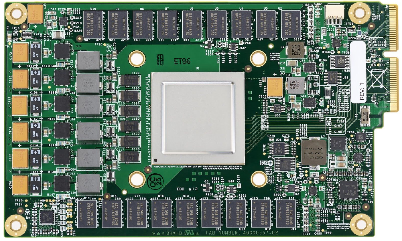
In data server environments, high-end devices are employed in order to maximize throughput at the penalty of substantial power consumption. A representative example is the NVIDIA Tesla V100 accelerator based on the NVIDIA Volta GV100 GPU (Fig. 12.3). The GV100 GPU employs the Volta architecture and is fabricated in a 12 nm production process at TSMC [11]. With a die size of 815 mm2 and a transistor count of 21.1 billion (25.9 million/mm2) it features 5120 shading units, 320 texture mapping units and 640 tensor cores which help improve the speed of machine learning applications. Tensor cores are specialized execution units designed specifically for performing the tensor/matrix operations that are the core compute function used in DNNs. The module comes with 16 GB GPU memory, 900 GB/s memory bandwidth, and a maximum of 300 W power consumption (1.3 GHz base clock, 1.5 GHz boost clock). Peak computation rates are 7.8 TFLOPS (Tera (1012) Floating point Operations per Second) of double precision floating-point (FP64) performance, 15.7 TFLOPS of single precision (FP32) performance, and 125 Tensor TFLOPS (FP16) [11]. Running VGG-16 on V100 yields from 821 (batch size 1) up to 2067 (batch size 128) cl/s [12].

NVIDIA Tesla V100 SXM2 Module (a) with Volta GV100 GPU (b) [11]
NVIDIAs Turing GPUs include a new version of the Tensor core design that has been enhanced with INT8 and INT4 precision modes for inference workloads that can tolerate quantization and don’t require FP16 precision. The TU104 graphics processor [13] includes 320 such Tensor cores, and is built on the 12 nm TSMC process with a die area of 545 mm2 and 13.6 billion transistors (25 million/mm2). The GPU is operating at a frequency of 585 MHz, which can be boosted up to 1.6 GHz. NVIDIA has placed 16 GB GDDR6 memory on the Tesla T4 graphics card. The card measures 168 mm in length, and features a single-slot cooling solution for a 70 W power consumption maximum [13]. Running VGG-16 on Tesla T4 with 726 (batch size 1) up to 1956 cl/s (batch size 128) is a bit slower compared to Tesla V100, but more power efficient: 10 (batch size 1) to 28 (batch size 128) cl/s/W instead of 4 (batch size 1) to 10 (batch size 128) cl/s/W [12].
NVIDIA T4 data servers deliver more than 10,000 TOPS (Trillion Operations per Second) for real-time speech recognition and other real-time AI tasks. NVIDIA also targets low-latency edge AI (Artificial Intelligence) with the scalable EGX platform [14], an accelerated computing platform that enables to perceive, understand and act in real time on continuous streaming data. NVIDIA EGX was created to meet the growing demand for instantaneous, high-throughput AI at the edge—where data is created—with guaranteed response times, while reducing the amount of data that must be sent to the cloud. EGX starts with the tiny NVIDIA Jetson Nano™, which in a few watts can provide 0.5 TOPS for tasks such as image classification, and it spans all the way to a full rack of NVIDIA T4 servers. NVIDIA supports programmers with its TensorRT™ platform for high-performance deep learning inference. It includes a deep learning inference optimizer delivering low latency and high-throughput for DNN inference applications. TensorRT™ is built on CUDA, NVIDIA’s parallel programming model, and optimizes neural network models trained in all major frameworks. Reduced precision inference significantly reduces application latency, which is a requirement for many real-time services in embedded applications. For example, optimizing VGG-16 with TensorRT™ for Jetson TX2 yield about 26 (FP16) or 13 cl/s (FP32) resulting in 3.4 or 1.7 cl/s/W, respectively (7.5 W) [15].
Currently, GPUs are the dominant hardware platforms for DNN learning and inference. Other GPU manufacturer (e.g. AMD, ARM, INTEL, Qualcomm) are offering powerful chips and programming frameworks for mapping DNNs on their GPUs as well. For example, Fig. 12.4 shows the AMD’s first 7 nm Vega GPU design improving performance per watt over previous generation products. It offers ultra-fast double precision performance with up to 7.4 TOPS (FP64) on the AMD Radeon Instinct™ MI60 Compute GPU. Optimized DNN operations with mixed FP16, FP32 and INT8 data representation support efficient learning and inference of DNNs. Two Infinity Fabric™ Links per GPU for high speed directly connected GPU clusters deliver up to 92 GB/s peer-to-peer bandwidth. Programmers are assisted by the ROCm open ecosystem that includes optimized libraries supporting frameworks like TensorFlow, PyTorch and Caffe 2 [16]. As benchmarking of inference accelerators is still in its infancy, a fair comparison of available GPUs is hard. Nevertheless, any of them can get the job efficiently done.

Chip micrograph of AMDs Vega GPU (7 nm CMOS, 1.6 GHz) [16]
GPUs offer powerful and scalable solutions for DNN acceleration. For uncompressed DNN models, layer operations are mapped with the help of frameworks to dense floating-point or integer matrix multiplications, which can be processed efficiently in parallel by GPUs. However, GPUs may perform poorly when operating on sparse data and compressed DNNs via fine-grained weight reduction [6, 7]. Hence, there is still room for architectural improvements and alternative solutions.
12.3 Field-Programmable Gate Arrays
Field-Programmable Gate Arrays have a modular and regular architecture containing mainly programmable logic blocks, embedded memory, and a hierarchy of reconfigurable interconnects for wiring the logic blocks. Furthermore, they may contain digital signal-processing blocks and embedded processor cores. After manufacturing, they can be configured before and during runtime by the customer. Today, system-on-chip designs with a complexity of about several billion logic gates and several megabytes of internal SRAM (Static Random Access Memory) can be mapped on state-of-the-art FPGAs. Clock rates approach the GHz range boosting the chip-computational power in the order of GOPS (billion operations per second) at a power consumption of several watts. Hence, FPGAs offer an interesting alternative for parallel implementation of DNNs providing a high degree of flexibility and a minimal time to market. The time for the development of an FPGA or application specific integrated circuit (ASIC) design is comparable. A big advantage of FPGAs is that no time for fabrication is needed. A new design can be tested directly after synthesis for which efficient CAD tools are available. A disadvantage of FPGAs is the slower speed, bigger area, and higher power consumption compared to ASICs. Compared to software implementations, FPGAs offer a higher and a more specialized degree of parallelization. Vendors of FPGAs, which have long been used to accelerate signal processing algorithms, are refining their products to suit DNN acceleration.
The implementation of DNNs on FPGAs makes it possible to realize powerful designs that are optimized for dedicated algorithms [18]. Another great advantage is the feature of reconfigurability that enables the change to a more efficient algorithm whenever possible. Using a lower precision allows to set up an optimized architecture that can be faster, smaller, or more energy-efficient than a high-precision architecture. For fine-tuning of DNNs, the FPGA can be reconfigured to implement high-precision elements. Additionally, the implemented algorithms can be adapted to the network size that is required for a certain problem. Thus, always the most suitable algorithms and architectures can be used. Furthermore, dynamic (or runtime) reconfiguration enables to change the implementation on the FPGA during runtime [19]. Dynamic reconfiguration is used to execute different algorithms on the same resources. Thus, limited hardware resources can be used to implement a wide range of different algorithms. In DNN simulations, we are often interested in providing as much computing power as possible to the simulation of the algorithm. But pre- and post-processing of the input and output data often also requires quite a lot of calculations. In this case, dynamic reconfiguration offers the opportunity to implement special pre-processing algorithms in the beginning, switch to the DNN simulation and in the end reconfigure the system for post-processing [20].
There are different approaches to implement DNNs on FPGAs, either the network itself is implemented on the FPGA or a DNN processing engine is developed for the FPGA onto which the target network is mapped at run-time. The advantage of the first approach is that it is possible to fully optimize the network for the target FPGA and achieve the best possible performance and energy efficiency. However, at the same time, this removes most forms of flexibility, as the design only works for one specific network and any changes to the network or the integration of a new network will result in several weeks of changing the design or require a complete redevelopment of the design. On the other hand, the DNN processing engine approach allows for any DNN model to be accelerated on the FPGA, as only the most common and performance critical layers are calculated on the FPGA and everything else on the CPU or on a different accelerator. Because the network is not calculated on the FPGA entirely, there will be at least some communication overhead which reduces the overall performance. Additionally, as this is a rather generic approach, the performance will be below that of a fully optimized implementation of the target network.
In many cases the DNN processing engine is the most suitable approach as it provides a high degree of flexibility. However, in situations where energy efficiency is of importance or when the FPGA needs to operate stand-alone, i.e., without a dedicated CPU, manually implementing the network on the FPGA will be the better choice.

Xilinx generic xDNN engine architecture for DNN inference [21]
One example of a hand optimized FPGA implementation, based on a Hardware Description Language (HDL), is presented in [22]. The authors developed an FPGA design of the VGG-16 network using a binary neuronal network (BNN). BNNs store their weights as either 0 or 1, which, even though a BNN requires a modification of the original VGG-16 architecture, significantly reduces the amount of weight storage required for the network. The developed design achieved a performance of 40.8 TOPS which equals to about 115 cl/s on an Intel Arria 10 GX1150 FPGA. Energy efficiency reaches 849.38 GOPS/W.
Other examples that fully implement the network on FPGA like [23, 24] aimed to design templates for High Level Synthesis (HLS). Convolutional layers usually have the highest computational cost in DNNs. In [23] Winograd and Fast Fourier Transformation (FFT) are implemented in processing elements (PEs) separately. Reuse of feature map data, pipelining and parallelization are applied as well. The authors are stating a performance of 2.5 TOPS for VGG-16 on the Xilinx ZC706 platform. In [24] also the Winograd optimization is applied to convolutional layers. Multiplications are simplified through the use of simple addition, subtraction or bit-shift operations, where possible. The implemented PEs are working in a systolic array and are organized in parallel working units. For VGG-16 a throughput of 3.8 TOPS on the Xilinx VCU118 is stated. A C3S network (3D CNN) is also implemented with the same HLS templates and achieves a 5× energy efficiency gain, compared to a GTX1080 GPU [24].
Convenient frameworks for high-level design support are an essential requirement for using FPGAs. High-level implementation tools, including Intel’s OpenCL Software Development Kit and Xilinx Vivado High-Level Synthesis, and Python-to-netlist neural network frameworks, such as DNN Weaver [25], make the DNN hardware design process for both FPGAs and ASICs faster and simpler. The OpenVINO toolkit developed by Intel [26] allows DNNs to be accelerated using MCPs, GPUs, FPGAs, and VPUs (Vector Processing Units), meaning that it is possible to determine and use the best possible accelerator for a given DNN or even for specific layers of that DNN. Out of the box, OpenVINO supports a large amount of different networks for execution on FPGAs, such as AlexNet, GoogleNet, VGG-16, ResNet, Yolo and many more. Additional networks can be manually implemented using Caffe, MXNet, TensorFlow, Kaldi or ONNX models. While Intel provides FPGA implementations for most of the commonly used layers, some layers are not available on FPGAs either because they are rarely used special layers, layers that do not significantly affect the performance or are new/custom developed layers. For those layers it is possible to either specify a fall-back implementation, e.g., on CPU/GPU, or to provide a custom implementation.
Xilinx develops two frameworks for DNN processing on FPGAs. One is the generic xDNN accelerator (Fig. 12.5) in the ML-Suite [21], which can in general be compared to Intels OpenVINO toolkit. The other is the FINN Framework from Xilinx Research Labs [27], which targets DNN inference specifically for quantized neural networks. Such frameworks allows DNN architects to migrate their designs to custom hardware with relative ease. Reconfigurability enables rapid design iteration, making FPGAs ideal prototyping and deployment devices for future DNNs developments.
12.4 Application-Specific Hardware
Application-specific integrated circuits (ASICs) have the highest potential for major improvements in resource-efficient performance for DNN inference. Many various special-purpose hardware implementations for DNN inference have been proposed and the number of proposals is still increasing. Advances in technology have successively increased the ability to emulate neural networks with speed and accuracy. Practically every processor vendor has specialized custom hardware for DNN acceleration. For digital ASICs, efficient software tools for a fast, reliable and implementation are available. Digital circuits can use standard technologies with the highest density in devices down to the lowest available structure sizes. Their time-consuming and resource-demanding fabrication processes, however, make it hard for them to keep up with the fast development of DNN algorithms.
One of the first custom ASICs for accelerating the inference phase of DNNs is Google’s Tensor Processing Unit (TPU) [30]. The TPU was designed as a co-processor on a standard PCIe bus, so that it can be plugged into a server like a GPU card (Fig. 12.6). The TPU chip is programmed in the TensorFlow framework to drive many important applications in Google data centres, including image recognition, language translation, search, and game playing. A first generation TPU chip is capable of performing 92 TOPS. The die size in 28 nm CMOS is below 330 mm2 and includes 28 MiB on-chip memory (29% of chip area), mainly for buffering neuron activations. The main logic block is the matrix multiply unit (24% chip area) with 256 × 256 8 Bit MAC operators. Clock speed is 700 MHz leading to 40 W measured power consumption when busy (28 W idle) [30]. As this first generation TPU was limited by memory bandwidth, the second generation design has an increased bandwidth of 600 GB/s. The second-generation TPUs can also calculate in floating point making them useful for both training and inference of DNNs. A third-generation TPU eight times as powerful as the second-generation TPUs is in use today (up to 100 Peta FLOPS) [30]. With its new Edge TPU Google offers an ASIC designed to offer DNN inference (INT8) for edge computing. The chip is much smaller and consumes far less power compared to the server TPUs. It is capable of performing 4 TOPS using 2 W resulting in about 130 cl/s for the VGG-16 DNN [31].

Besides application in data centres, DNN accelerators hold much promise for edge computing. Embedded Machine Learning (ML) at the edge can be applied to almost every electronic appliance, from production lines (industry 4.0) over house hold devices (smart home) to hand-held devices (smartphones). Applications that require resource-efficient implementations with respect to latency, power, and cost. Mobile devices are more and more equipped with sensors and embedded data processing (e.g. face detection, voice and gesture recognition, activity tracking, …). For data processing ML methods as DNNs take over the lead and can be found in almost all new smartphones today. Hence, any smartphone vendor includes ML accelerators in their mobile SoC devices nowadays; e.g., Qualcomm in Snapdragon [33], HiSilicon in Kirin [34], Samsung in Exynos [35], or MediaTek in Helio [36]. A detailed analysis of DNN accelerators in smartphone SoCs can be found on the regularly updated official project website maintained by Andrey Ignatov (ETH Zurich, Computer Vision Lab, [37]).
For example, the Neural Processing Unit (NPU) from Samsung for their Exynos SoCs [35] features an energy-efficient butterfly-structure dual-core accelerator offering 1024 MAC operations (INT8) and three-fold parallelism in computing DNNs. The NPUs are optimized for DNN inference. The overall architecture of one NPU core is shown in Fig. 12.7. Each core has 16 arrays of dual-MAC units, performing 512 MAC operations in total. The NPU in Exynos occupies 5.5 mm2 (8 nm CMOS technology) and operates at 0.5 to 0.8 V supply voltage, 67 to 933-MHz clock frequency [35]. The NPU is able to support compressed DNNs (sparsity in weights and activations). The NPU controller (NPUC) automatically configures the two cores and traverses the DNN. A DMA unit manages the compressed weights and feature maps in each of the scratchpads of the cores. Skipping zero weights and activations increases throughput. The measured performance is 6.9 TOPS and 3.5 TOPS (with 75% zero-weights) for 5 × 5 and 3 × 3 convolutional kernels, respectively. The energy efficiency is 11.5 and 8.4 TOPS/W for 5 × 5 and 3 × 3 kernels, respectively [33]. Running an Inception-v3 network (similar model size as VGG-16) the energy efficieny is measured as 3.4 TOPS/W. At 933 MHz the two NPUs add up to nearly 1 TMAC/s or 2 TOPS resulting in about 65 cl/s and 43 cl/s/W of the VGG-16 implementation for ImageNet data.

Besides processor vendors, many IP vendors (ARM, Synopsis, Imagination, Cadence, VeriSilicon, …) offer IP-blocks for DNN inference acceleration. For example, Cadence offers the Tensilica DNA processor IP (Intellectual Property) for AI inference [39]. The architecture incorporates a hardware engine and a Tensilica DSP (Vision C5). Heart of the hardware engine is a 4 K MAC array configuration with up to 3.4 TMAC/s/W in 16 nm. A single DNA 100 processor scales from 0.5 to 12 TMACs (INT8). Multiple processors can be stacked to achieve hundreds of TMACs. A Tensilica Neural Network Compiler maps a trained ANN into executable and optimized code. A SystemC model is provided for cycle-accurate system simulations [39]. Based on the estimated 3.4 TMAC/s/W a VGG-16 implementation on a DNN 100 may achieve about 110 cl/s/W.
Many startups come up with special architectures for DNN acceleration as well. They range from processor-in-memory computing (Mythic, Syntiant, Gyrfalcon) to processor-near-memory (Hailo): from programmable logic (Flex Logix) to RISC-V cores (Esperanto, GreenWaves); and from the tiny (Eta Compute) to the hyper-scale (Cerebas, Graphcore). Most of them aim for ML at the edge. For example, the Goya™ HL-1000 chip is an inference chip being developed by startup Habana Labs [40]. The scalable Goya platform architecture has been designed from the ground up for deep learning inference workloads. It comprises a fully programmable Tensor Processing Core (TPC™) along with its associated development tools, libraries and compiler. The platform is capable of massive data crunching with low latency and high accuracy. The TPC™ was designed to support deep learning workloads. It is a VLIW SIMD vector processor with ISA and hardware that was tailored to serve deep learning workloads efficiently. The HL-1000 chip uses a cluster of eight TPC™ cores and further dedicated hardware. The TPC™ natively supports several mixed-precision data types (FP32, INT32, INT16, INT8, UINT32, UINT16, UINT8). The performance achieved on VGG-16 inference is 1447 cl/s (batch size 1) with 1.1 ms latency [40]. More detailed Information on the architecture or about power consumption are currently not unavailable.
The Graphcore wafer-scale approach from Cerebas is another start-up example at the extreme end of the large spectrum of approaches [41]. The company claim to have built the largest chip ever with 1.2 trillion transistors on a 46,225 mm2 silicon wafer (TSMC 16 nm process, Fig. 12.8). It contains 400,000 ML optimized cores, 18 GB on-chip memory, and 9 PetaByte/s memory bandwidth. The programmable cores with local memory are optimized for ML primitives and equipped with high-bandwidth and low latency connections. DNN approximations are incorporated, such as fine grained sparsity. The 2D mesh topology is a fully configurable fabric with hardware supported communication. The entire wafer operates on a single DNN and supports learning. Common ML-frameworks (e.g. Tensorflow, PyTorch) can be used for programming the wafer engine, Cerebas tools map, place, and route the network layers onto the wafer. Redundancy for cores and links can be incorporated to replace defective elements [41]. The company announced that the system is running customers workload, but more detailed information on the architecture and performance data are not published yet.

Last but not least, academia is very active in the DNN chip landscape as well. Examples are the Eyeriss architecture from MIT [43], ENVISON from KU Leuven [44], STICKER-T from Tsinghua [45], or DNPU from KAIST [46]. The architectures have in common a 2d-array of special processing elements and controllers for an efficient data flow from and to the memory. For example, the ENVISION chip from KU Leuven is equipped with 2D- (for convolutions) and 1D-SIMD arrays (for ReLU, max-pooling), and a scalar unit (Fig. 12.9). An on-chip memory (DM) consists of 64 × 2 kB single-port SRAM macros which can be read or written in parallel [44]. The processor has a 16 bit SIMD instruction set extended with custom instructions. The chip is divided into three power- and body-bias domains to enable granular dynamic voltage scaling. Implemented in a 28 nm FDSOI technology on 1.87 mm2, the chip runs at 200 MHz at 1 V and room temperature. Energy-efficiency is further improved by modulating the body bias in an FDSOI technology. This permits tuning of the dynamic versus leakage power balance while considering the computational precision. Efficiency is 2 TOPS/W on average for VGG-16 (about 13 cl/s/W) and up to 10 TOPS/W peak (about 64 cl/s/W).

Top level architecture of the ENVISON DNN accelerator (a) and chip micrograph (b) [44]
In conclusion, the DNN accelerator development is progressing fast with a steady stream of new architectures coming up. At first, the acceleration of the data flow had the highest priority. A range of customized blocks of large parallel arrays multiply-add units for efficient and flexible computation of the many convolutions and fully connected layers were proposed. As DNNs got larger, the circuit designers realized that memory access and data movement are more critical than arithmetic. Additional circuitry like buffers, transpose logic, nonlinearity logic must be employed to keep the MAC units busy while utilizing the memory bandwidth efficiently. With even larger networks DNN approximation and compression is used in order to match the application requirements for throughput, latency and energy efficiency. Counterintuitively with the growth of model size and complexity, it has been shown that out of the millions of parameters used in common DNN architectures, many of these can be removed with insignificant reductions in accuracy, leading to a much lower memory footprint for storing the model as well as less computations and significantly lower energy usage. This process is referred to as pruning and can be applied to both connection weights and neurons and there are various methods proposed in the literature [6, 7]. Another popular method to increase the efficiency reduces the numerical precision of weights and activations. This method is called quantization. Typically, single precision floating point numbers are used to represent weights and activations. However, networks with ternary weights (+1, 0, and −1) show in some cases only low performance loss when compared to the floating-point counterparts. In addition to pruning and quantization, there are many other methods that can be used to make DNN accelerators more efficient. However, combining these, in some cases contradictive methods, in an optimal way, as well as optimising a model to meet system requirements, is still an unsolved problem. Hence, system designers should jointly consider hardware/software issues for finding optimal compromises, so called pareto-optimal architectures for efficient and flexible implementation of DNN accelerators. The “AI chip landscape” [47] is not settled yet.
12.5 Benchmarking
There is a tremendous surge of innovation in DNN hardware, making it a very challenging task choosing the best hardware offering for a given application. Hardware vendors have yet no incentive to provide unbiased comparison and benchmarking. Hence, there is a high demand for benchmarking, the objective performance measuring based on specific indicators, of such systems. Though benchmarking of DNN accelerators is still in its infancy, there are first approaches to fill this gap. Baidu and Google together with researchers from several universities launched the MLPerf benchmark suite in May 2018 in part to create a fair way to measure the chips expected from “dozens and dozens” of startups. The MLPerf approach is supported by over 50 companies and researchers from 7 universities [48]. Hence, it has a chance to become for AI accelerators what SPEC benchmark is for CPUs. The suite itself consists of two major subparts: training and inference benchmarks. At time of writing, the suite is still in beta stadium (v0.6) and inference results are available only for a previous version of the suite. Training results can be found on their webpage [48]. Main metric of all benchmarks is the wallclock time to reach a pre-defined goal using a pre-defined network model (e.g. a certain accuracy on a machine learning task). The set of benchmarks comes together with a set of rules for submitting results, and most importantly, results have to be submitted together with the source code. This allows to reproduce the results to some extent if the respective hardware is at your disposal.
For smartphones based on Google’s Android operating system and Mobile SoCs in general there is the AI-Benchmark [49]. Since 2019, the suite is also capable of benchmarking CPUs, GPUs and TPUs based on Tensorflow, allowing to compare workstation hardware with mobile hardware. The suite is focusing on inference and consists of 21 tests distributed over 11 benchmark sections. The overall rules are not that strict compared to the MLPerf approach. However, in this case benchmarking is strongly coupled to the implementation of the networks, relying on frameworks and drivers to efficiently map individual networks to the hardware. Results in the form of a ranking can be found online [50]. A similar approach is applied by the EEMBC MLMark benchmark library [51]. Instead of using the measured wallclock time as a benchmark metric, MLMark measures throughput, latency and accuracy targeting requirements of embedded applications. Currently, the suite consists of three models only: MobileNet [52], MobileNet-SSD and ResNet-50. The results are visible to registered members only.
One major point, when it comes to embedding DNN accelerators, is not only the wallclock time per inference or latency, which is constrained by e.g. real-time requirements of your application, but also the resource-efficiency. Mobile applications, like autonomous driving, robot control or everyday tasks on a smartphone, require resource-efficient implementations for DNN inference. Despite these demands, this benchmark measure is not served by any of the discussed benchmark approaches. The cost of employing a system of multiple GPUs/TPUs is also a very restricting factor in training deep networks, which is also not considered by any of the suites.
DNNs are a field with rapid development. This complicates representative and up-to-date benchmarking of hardware accelerators, which is reflected in the state of all machine learning benchmark suites. The performance of a DNN platform depends on many aspects, such as computational accuracy or tool assistance. A special architecture may perform well on a DNN of type A, but worse on another of type B. At present, a fair comparison is almost impossible. Only few chips have been fully described and benchmarked (e.g. Google’s TPU) but the pipeline of new implementations is full.
In Fig. 12.10 the performance values of the introduced DNN accelerators (Tables 12.1, 12.2, 12.3) implementing VGG-16 have been merged. The expected clustering from low end edge devices over FPGA implementations to high end ASICs and GPUs can roughly be seen. The effect of the batch size is clearly visible [e.g. V100: 821 cl/s (batch size 1) up to 2845 cl/s (batch size 128)] as well. However, such figures have to be considered with caution. First of all, most of the data have been taken directly from the publications and are not a result of an objective benchmark measurement. In most cases it is unclear how these data are obtained. Especially, power data are in most cases missing. Second, though the comparison is based on a fixed DNN model (VGG-16) and data set (ImageNet) there are many additional architectural and technological attributes influencing the performance data. Obviously, the numeric precision for weights and activations plays an important role (e.g. Jetson TX2 about 13 cl/s for FP32 and 26 cl/s for FP16) as well as the data flow management. The size and the utilization of the implemented MAC arrays are essential as well. Utilization in this context is the percentage of the raw compute capabilities of the system that can be effectively used for a real workload (DNN model). Utilization varies with the DNN model, but utilization figures are rarely published. A high peak performance of an accelerator is no guarantee for a high inference performance. Last but not least, the framework used for DNN implementation has a high impact on inference performance (e.g. Jetson TX2 FP32 6 cl/s using TensorFlow and 13 cl/s using TensorRT).

Comparison of VGG-16 implementation results of selected accelerators
12.6 Outlook
Parallel standard hardware like multi-core MPCs, GPUs, or FPGAs are cost effective, available, and benefit from market-driven development improvements in the future. They have the highest flexibility and are manufactured in standard technologies with highest device densities. They set the base-line with respect to cost and performance for DNN implementation. ASICs have the highest potential for major improvements in resource-efficient performance for DNNs. Currently, product developers and users have few real choices for hardware supporting efficient DNN implementation. Almost all major IT and chip companies are aggressively entering the market. However, the increased competition doesn’t necessarily mean better choices, as customers still don’t have the means to evaluate these different chipset platforms for the optimal integration with their AI-driven system and application demands.
Due to their highly regular and modular structure, inherent fault-tolerance, and learning ability, ANNs offer an attractive alternative for ultra-large-scale integration and the development of resource-efficient systems with minimal total energy consumption combined with a small size and fault-tolerant behaviour. Among the many different ANN models discussed in literature (see e.g. “The Neural network Zoo” [53]) DNNs serve in this chapter as a representative example architecture. Despite the impressive development of nanoelectronics during the last decades, there is still no clear consensus on how to exploit this technological potential for massively-parallel ANN implementations. Hence, it is currently quite difficult to determine the best way to perform DNN calculations for any given application. This is one reason for the huge variety of approaches to DNN hardware implementation known today.
DNNs look promising but have many variations, and the algorithms are still in development, so it is not clear how they may influence hardware development in the future. Implementations are still incomplete and immature. There is a lack of standardization, e.g. for model data formats, file formats to transfer models and data sets between frameworks, or interfaces to build engineering tools that work together. A first step in this direction is the specification of the Brain Floating Point (BFLOAT16) half-precision data format for DNN learning [54]. Its dynamic range is the same as that of FP32, making conversion between both straightforward, and training results are almost the same as with FP32. Industry-wide adoption of BFLOAT is expected.
Another challenge lies in mastering the design complexity and achieving economic viability for integrated systems with more than a billion devices per square centimetre. This requires system concepts that both exhaust the possibilities of future technologies and reduce the design- as well as the test-complexity. These arguments were already a strong motivation for ANN hardware in the 80s [55]. Flexibility is another important factor as researchers are coming up with ANN concepts all the time. While DNNs are the dominant model especially for image processing today, other types of ANN models are more suited to other applications, such as speech recognition or controlling tasks. Hence, today´s accelerators may be too specialized to accelerate future ANN models. The challenge is to find the right balance of flexibility, performance, and price for as many applications as possible. This should go hand in hand with efficient software frameworks for developers and users of ANN hardware in this rapidly evolving sector.
In conclusion, as the increase in processor speed slows down alternative architectures get a second chance today. The hunt for the right architecture is just beginning. As in the late 80s [56], within the second neural network hype, analogue computing, wafer-scale integration, 3D-integration, in-memory computing, massively parallelism, and even optical approaches are being explored again. Radically new ideas for circuit designs or system architectures are not in sight. At present, know-how from digital signal processing and data flow management from massively parallel computing architectures are combined in different ways. An obvious approach is to bring the memory closer to the arithmetic devices to mitigate the memory bottleneck and reduce power consumption. In-Memory-Computing (IMC) exploiting dense 2D memory arrays and matrix-vector multiplication offer an interesting alternative approach to achieve high throughput with low power requirements for DNN accelerators [57,58,59]. However, model sizes of today’s DNNs are generally too large to fit into on-die memory resources. On-die memory can be used to mitigate the memory bandwidth problem, but deciding what stays on-die versus off-die requires careful memory management to achieve high performance. Even more computational power may be obtained by emerging technologies like quantum computing, molecular electronics, or novel nano-scale devices (memristors, spintronics, nanotubes (CMOL)), but these technologies will not be available on broad basis in the next decade. Today, we are still early in the efficient use of nanoelectronics, and we are keenly awaiting the technology we can use tomorrow.
References
K. Simonyan, A. Zisserman, Very deep convolutional networks for large-scale image recognition. arXiv:1409.1556v6 (2015)
D. Gschwend, ZynqNet: an FPGA-accelerated embedded convolutional neural network. Masters Thesis, ETH Zürich (2016)
V. Sze et al., Efficient processing of deep neural networks: a tutorial and survey. arXiv:1703.09039 (2017)
O. Russakovsky et al., ImageNet large scale visual recognition challenge. arXiv:1409.0575v3 (2015)
T.L.I. Sugata, C.KJ. Yang, Leaf App: leaf recognition with deep convolutional neural networks. In: IOP Conf. Series: Materials Science and Engineering, vol. 273 (2017)
E. Wang et al., Deep neural network approximation for custom hardware: where we’ve been, where we’re going. ACM Comput. Surv. 52(2), Article 40 (2019)
Y. Cheng et al., Model compression and acceleration for deep neural networks: the principles, progress, and challenges. IEEE Signal Process. Mag. 35, 1 (2018)
M. Gerland et al., Parallel computing experiences with CUDA. IEEE Micro 28(4), 13–27 (2008)
J.E. Stone et al., OpenCL: a parallel programming standard for heterogeneous computing systems. Comput. Sci. Eng. 12(3), 66–72 (2010)
K.S. Oh, K. Jung, GPU implementation of neural networks. Pattern Recognit. 37(6), 1311–1314 (2004)
NVIDIA, TESLA V100 GPU Architecture, Whitepaper (2017)
https://developer.nvidia.com/deep-learning-performance-training-inference (retrieved 31.10.2019)
NVIDIA, Turing GPU Architecture, Whitepaper, (2018)
https://www.nvidia.com/en-us/data-center/products/egx-edge-computing/ (retrieved 31.10.2019)
https://github.com/NVIDIA-AI-IOT/tf_to_trt_image_classification (retrieved 31.10.2019)
https://www.amd.com/en/technologies/vega7nm (retrieved 31.10.2019)
M. Almeida et al., EmBench: quantifying performance variations of deep neural networks across modern commodity devices. arXiv:1905.07346v1 (2019)
A.R. Omondi, J.C. Rajapakse (eds.), FPGA Implementations of Neural Networks (Springer, Berlin, 2005)
M. Koester et al., Design optimizations for tiled partially reconfigurable systems. IEEE Trans. Very Large Scale Integr. Syst. 19(6), 1048–1061 (2010)
M. Porrmann, U. Witkowski, U. Rückert, Implementation of self-organizing feature maps in reconfigurable hardware, in FPGA Implementations of Neural Networks, ed. by A.R. Omondi, J.C. Rajapakse (Springer, Berlin, 2005), pp. 253–276
https://github.com/Xilinx/ml-suite/blob/master/docs/ml-suite-overview.md (retrieved 31.10.2019)
D.J.M. Moss et al., High performance binary neural networks on the Xeon + FPGA™ platform, in 27th International Conference on Field Programmable Logic and Applications (FPL), Ghent (2017), pp. 1–4
Y. Liang, L. Lu, Q. Xiao, S. Yan, Evaluating fast algorithms for convolutional neural networks on FPGAs. IEEE Trans. Comput.-Aided Des. Integrat. Circuits Syst. https://doi.org/10.1109/tcad.2019.2897701 (2018)
J. Shen, Y. Huang, M. Wen, C. Zhang, Towards an efficient deep pipelined template-based architecture for accelerating the entire 2D and 3D CNNs on FPGA. IEEE Trans. Comput.-Aided Des. Integrat. Circuits Syst. https://doi.org/10.1109/tcad.2019.2912894 (2018)
H. Sharma et al., From high-level deep neural models to FPGAs, in IEEE/ACM International Symposium on Microarchitecture (2016)
https://docs.openvinotoolkit.org (retrieved 31.10.2019)
M. Blot et al.: FINN-R: an end-to-end deep-learning framework for fast exploration of quantized neural networks. arXiv:1809.04570v1 (2018)
J. Zhang, J. Li, Improving the performance of OpenCL-based FPGA accelerator for convolutional neural network, in Proceedings of the 2017 ACM/SIGDA International Symposium on Field-Programmable Gate Arrays (FPGA ‘17). ACM, New York, NY, USA, 25–34 (2017)
C. Zhang et al., Caffeine: towards uniformed representation and acceleration for deep convolutional neural networks. IEEE Trans. Comput. Aided Des. Integrat. Circuits Syst. 38(11), 2072–2085 (2019)
P. Norman et al., A domain-specific architecture for deep neural networks. Commun. ACM 61, 9 (2018)
A. Reuther et al., Survey and benchmarking of machine learning accelerators. arXiv:1908.11348v1 (2019)
https://images.anandtech.com/doci/12195/google-tpu-board-2.png (retrieved 31.10.2019)
https://www.qualcomm.com/snapdragon (retrieved 31.10.2019)
http://www.hisilicon.com/en/Solutions/Kirin (retrieved 31.10.2019)
J. Song et al., An 11.5TOPS/W 1024-MAC butterfly structure dual-core sparsity-aware neural processing unit in 8 nm flagship mobile SoC, in Proceeding of the IEEE International Solid-State Circuits Conference (2019), pp. 130–132
https://i.mediatek.com/P60 (retrieved 31.10.2019)
http://ai-benchmark.com (retrieved 31.10.2019)
L. Gwennap, EXYNOS 9820 has Samsung AI Engine, Microprocessor Report (11 March 2019)
https://ip.cadence.com/ai, (retrieved 31.10.2019)
Habana Labs, Goya™ Inference Platform White Paper (2019)
https://www.graphcore.ai (retrieved 31.10.2019)
M. Demler, CEREBRAS BREAKS THE RETICLE BARRIER: Wafer-Scale Engineering Enables Integration of 1.2 Trillion Transistors, Microprocessor Report (2 Sept 2019)
Y-H. Chen et al., Eyeriss: an energy-efficient reconfigurable accelerator for deep convolutional neural networks. IEEE J. Solid-State Circuits 52(1), 127–138 (2016)
B. Moons et al., ENVISION: a 0.26-to-10TOPS/W subword-parallel dynamic-voltage-accuracy-frequency-scalable convolutional neural network processor in 28 nm FDSOI, in Proceeding of the IEEE International Solid-State Circuits Conference (2017), pp. 146–148
J. Yue et al., A 65 nm 0.39-to-140.3TOPS/W 1-to-12b unified neural-network processor using block-circulant-enabled transpose-domain acceleration with 8.1 × higher TOPS/mm2 and 6T HBST-TRAM-based 2D data-reuse architecture, in Proceeding of the IEEE International Solid-State Circuits Conference (2019), pp. 138–140
D. Shin et al., DNPU: An 8.1TOPS/W reconfigurable CNN-RNN processor for general-purpose deep neural networks, in Proceeding of the IEEE International Solid-State Circuits Conference (2017), pp. 140–142
https://basicmi.github.io/AI-Chip/ (retrieved 31.10.2019)
MLPerf: https://mlperf.org/ (retrieved 31.10.2019)
A. Ignatov et al., AI benchmark: all about deep learning on smartphones in 2019. ariv.191006663v1 (2019)
http://ai-benchmark.com/ (retrieved 31.10.2019)
https://www.eembc.org/mlmark/ (retrieved 31.10.2019)
A.G. Howard et al., Mobilenets: efficient convolutional neural networks for mobile vision applications. arXiv preprint arXiv:1704.04861 (2017)
https://www.asimovinstitute.org (retrieved 31.10.2019)
D. Kalamkar et al., A study of BFLOAT16 for deep learning training. arXiv:1905.12322v3 (2019)
U. Ramacher, U. Rückert (eds.), VLSI Design of Neural Networks (Kluwer Academic, Boston, 1991)
P. Inne, in Digital Connectionist Hardware: Current Problems and Future Challenges, Biological and Artificial Computation: From Neuroscience to Technology. Lecture Notes in Computer Science, vol. 1240 (Springer, Berlin, 1997), pp. 688–713
N. Verma et al., In-memory computing: advances and prospects. IEEE Solid-State Circuits Mag. 11(3), 43–55 (2019)
C. Eckert et al., Neural cache: Bit-serial in-cache acceleration of deep neural networks. IEEE Micro 2019, 11–19 (2019)
X. Si et al.: A twin-8T SRAM computation-in-memory macro for multiple-bit CNN-based machine learning, in Proceeding of the IEEE International Solid-State Circuits Conference (2019), pp. 396–398
Author information
Authors and Affiliations
Corresponding author
Editor information
Editors and Affiliations
Rights and permissions
Copyright information
© 2020 Springer Nature Switzerland AG
About this chapter

Cite this chapter
Rueckert, U. (2020). Digital Neural Network Accelerators. In: Murmann, B., Hoefflinger, B. (eds) NANO-CHIPS 2030. The Frontiers Collection. Springer, Cham. https://doi.org/10.1007/978-3-030-18338-7_12
Download citation
DOI: https://doi.org/10.1007/978-3-030-18338-7_12
Published:
Publisher Name: Springer, Cham
Print ISBN: 978-3-030-18337-0
Online ISBN: 978-3-030-18338-7
eBook Packages: Physics and AstronomyPhysics and Astronomy (R0)