
Abstract
For nano scale logic circuit, device area and power consumption are the major concerns. In this paper, the design of an optimized SISO shift register is explored based on quantum-dot cellular automata (QCA) device. The design is achieved in a single layer. To design the shift register circuit, a new QCA D flip-flop has been proposed. These new D flip-flop has minimum cell count and lower device area over existing designs. The proposed shift register also outperforms the existing designs by reducing cell count and area. The power consumption by the proposed design is carried out that shows the low energy consumption nature of the circuit. Logic gate, QCA cell and device density have been considered to evaluate the circuit. Simulation timing diagram and truth table of the proposed circuits are compared which shows that all the designs are functioning efficiently. Stability under thermal randomness for all the designs are analyzed which shows the steadiness of the designs. The impacts of control input, i.e., clock on the designs are explored. Besides the defects in proposed QCA layouts are also identified and excelled for fault free implementation.
1 Introduction
The enhancements in integration, operating speed, and power consumption of integrated circuits have been achieved by nanoelectronics engineering through past several decades. The enhancement is achieved with reducing the attribute size of different semiconducting components (Lent and Tougaw 1997; Lent et al. 2006; Kianpour and Sabbaghi-Nadooshan 2014; Tehrani et al. 2013; Hashemi and Navi 2014). But decrease in transistor size caused problems like excessive heat dissipation. As an alternative solution, QCA technology was invented by Lent and Tougaw (1997). QCA is a promising nanotechnology that can encode binary data beyond current switches. It has high circuitry areas, low power consumption and faster switching speed (Das and De 2010, 2011, 2012; Das et al. 2015, Das et al. 2016). The information in QCA circuit is possessed in the form of charge on electrons (Pradhan and De 2013; Thapliyal and Ranganathan 2010; Thapliyal et al. 2013; Das and De 2015a, b). The columbic interaction between each QCA cell is responsible for information to carry from input to output within QCA circuit (Sardinha et al. 2013; Arjmand et al. 2013; Ghosh et al. 2014a, b, 2015). To store digital information, registers are essential component. This paper shows an optimized design and implementation of D flip-flop and 3-bit serial-in-serial-out (SISO) shift register using QCA.
This paper has the contributions as follows.
-
1.
A new QCA layout of D flip-flop.
-
2.
Optimized design of SISO shift register in QCA using proposed D flip-flop.
-
3.
The detailed comparison of proposed D flip-flop and shift register circuit with existing layouts are explored. During comparison, cell count and device density are considered.
-
4.
Defects in proposed QCA layouts are identified and excelled. To detect those defects, test vectors are also proposed.
-
5.
The power consumption by the proposed designs is estimated.
-
6.
The stability of the layouts under thermal randomness is also deliberated.
-
7.
The impact of control input i.e., clock on the designs are also explored.
The paper is oriented as follows. Section 2 shows QCA overviews. The design and implementation of proposed D flip-flop and 3-bit SISO shift register based on QCA is describe in Sect. 3. Section 4 outlines the simulation outputs including design complexity, comparison with existing layouts, power dissipation estimation and stability analysis of the proposed circuits under thermal randomness. At the end, the conclusion is drawn in Sect. 5.
2 QCA overview
A QCA cell consists of four quantum dot lies at the four corner of the cell as shown in Fig. 1a. Each of these cell occupies two mobile electrons (Lent et al. 2006; Kianpour and Sabbaghi-Nadooshan 2014; Hashemi and Navi 2014). Depending on the electronic charge of the electrons, the QCA cell possesses its polarization. Two polarized states are P = +1 and P = −1 respectively, and the binary information stored within them is 1 and 0 respectively. P = 0 means an un-polarized cell, i.e., the cell does not contains any information (Ghosh et al. 2014b; Das et al. 2012, 2013; De et al. 2013). Majority voter (MV) (Das et al. 2013; Silva et al. 2015; Sen et al. 2014; Pudi and Sridharan 2011; Debnath et al. 2016a, b) is the main building block of QCA circuit. It consists of five cells as shown in Fig. 1b. The logic expression for MV is obtained in Eq. (1)

QCA cell and logic gates a QCA cell structure, b majority voter c AND gate and OR gate d QCA 90° wire and 45° wire, e inverter
When one of the inputs of the MV is set to ‘0’, the logic AND-gate is formed and if it is set to ‘1’, logic OR gate is produced as shown in Fig. 1c. QCA wire (Arjmand et al. 2013; Ghosh et al. 2014a) can be constructed by placing QCA cell sequentially as given in Fig. 1d. Larger circuit is produced in combination of QCA wire with the MV. When QCA cells are placed at 45°, they act as a NOT gate which is shown in Fig. 1e (Ghosh et al. 2014b; Das et al. 2012; Das and De 2016a, b, c, d, e, f, g).
3 Proposed work
3.1 QCA based D flip-flop
D flip-flop (Nelson et al. 1995) is a combinational circuit having one input and two outputs as shown in Fig. 2. Its characteristic expression is Q(t + 1) = D, where Q(t + 1) represents the next state after every clock pulse. The truth table of D flip-flop is explored in Table 1. D flip-flop is basically R–S flip-flop having an inverter in place of input R. The inverter reduces the number of input of R–S flip-flop from two to one to form a D flip-flop. The proposed QCA schematic of D flip-flop and its QCA layout are shown Fig. 3a and b respectively. The structure of D flip-flop is achieved using a closed loop. Each QCA cell value within the loop stays in their current polarization until the clock value is altered. To design the circuit 3 MVs, 1 inverter, 23 QCA cell and 4 clocking zones are used. The latency of the circuit is 1. The simulation result is explored in Fig. 4. Outputs corresponding to inputs in Fig. 4 are shown by the arrow which describes that the required outputs are appeared after second clock pluses. The result is verified with the truth table as shown in Table 1. This verification confirms the accuracy of the circuit.

Block representation of D flip-flop

D flip-flop a QCA schematic b QCA layout

Simulation result of proposed D flip-flop
3.2 QCA based SISO shift register
A sequential circuit which can store and possess the digital data is called shift register (Nelson et al. 1995). Depending on the clock pulse, shift register advances the input signal from one bit to next MSB bit. Figure 5 shows a 3-bit SISO shift register, composed of three D flip-flops connected in a chain. The output of one flip-flop is used as an input to next flip-flop. All the flip-flops are driven through a common clock, and all are also set or reset concurrently. In Fig. 5, Q1 and Q2 are the intermediate states. Q3 is the final output state. The proposed QCA schematic of shift register and its QCA layout are shown in Fig. 6a and b respectively. The QCA structure of 3-bit shift register is achieved by cascading three QCA D flip-flops. The layout consists of 9 MVs, 3 inverters, and 100 QCA cell. The latency of the circuit is 3. The simulation result is plotted in Fig. 6c. The arrows in Fig. 6c are used to show the outputs for each intermediate states and the final state corresponding to the inputs. The result is verified with theoretical values. This verification confirms the accuracy of the circuit.

Block diagram of 3-bit SISO shift register

Proposed 3-bit SISO shift register a QCA schematic, b QCA layout, and c simulation result
3.3 Impact of control input (Clk) on proposed designs
In this section the impact of control input (Clk) on the proposed designs are analyzed and explored. To perform this analysis, the layouts of proposed QCA D flip-flop and shift register as shown in Figs. 3a and 6a respectively are restructured. The new structures are based on individual input to different MVs which are shown in Fig. 7a and b respectively. Using this figures, the impact of control input (Clk) on proposed designs are observed and explored through Sects. 3.3.1 and 3.3.2 respectively.

Individual input based restructure schematic of a Proposed QCA D flip-flop and b Proposed 3-bit SISO shift register
3.3.1 Impact of control input (Clk) on proposed D flip-flop
The impact of control input (Clk) on the proposed D flip-flop, i.e., the changes in output due to Clk is described in this section. The analysis is performed considering different clock status at the Clk. Suppose the input at Clk is stuck-at-0. Then the impacts on the output signal are as follows.
-
The inputs of MV M1 in Fig. 7a are as 0, D and 0 which results that the output of MV M1, q1, becomes 0.
-
The inputs of MV M2 are as Q, 1 and 0 which results that MV M2 will have the output, q2, becomes equal to Q.
-
The inputs of MV M3 are as q1, 1 and q2, i.e., 0, 1 and Q respectively, which results that the output of MV M3, Q, becomes same as Q.
The result is shown in Table 2. Similarly, for different input status at the Clk, the impact on the output signal is carried out and explored through Table 2.
3.3.2 Impact of control input (Clk) on proposed SISO shift register
This section illustrates the impact of Clk on the proposed SISO shift register, i.e., the changes in output due to Clk. The analysis is performed considering different clock status at the Clk. Suppose the input at Clk is stuck-at-0. Then the impacts of control input (Clk) on SISO shift register, i.e., the changes in output due to control input are as follows.
-
The inputs of MV M1 in Fig. 7b are as 0, D and 0 which results that the output of MV M1, q1, becomes 0.
-
The inputs of MV M2 are as 1, 0 and O1 which results that MV M2 will have the output, q2, becomes equal to O1.
-
The inputs of MV M3 are as q1, 1 and q2 i.e., 0, 1 and O1 respectively, which results that the output of MV M3, O1, becomes same as O1.
-
The inputs of MV M4 are as 0, O1 and 0 which results that the output of MV M4, q3, becomes 0.
-
The inputs of MV M5 are as 1, 0 and O2 which results that MV M5 will have the output, q4, becomes equal to O2.
-
The inputs of MV M6 are as q3, 1 and q4 i.e., 0, 1 and O2 respectively, which results that the output of MV M6, O2, becomes equal to O2.
-
The inputs of MV M7 are as 0, O2 and 0 which results that the output of MV M7, q5, becomes 0.
-
The inputs of MV M8 are as 1, 0 and O3 which results that MV M8 will have the output, q6, becomes equal to O3.
-
The inputs of MV M9 are as q5, 1 and q6 i.e., 0, 1 and O3 respectively, which results that the output of MV M9, O3, becomes same as O3.
The result is shown in Table 3. Similarly, for different status at the Clk, the impact on the output signal is carried out and excelled through Table 3.
4 Result and discussions
The design as well as simulation of the proposed layouts has been performed on QCA Designer simulation tool (Walus et al. 2004). Parameters which are considered during simulation are shown in Fig. 8. The dimension of each QCA cell is 18 nm × 18 nm. The coherence vector technique and Euler method are employed during simulation.

List of parameters
4.1 Comparison with existing layouts
The comparison of proposed QCA D flip-flop and shift register circuit with previously reported designs in terms of circuit complexity are shown in Tables 4 and 5, respectively. Table 4 describes that the proposed QCA circuit of D flip-flop has less cell count and high device density than existing ones (Mustafa and Beigh 2014; Ahmad et al. 2014; Goswami et al. 2014; Lim et al. 2012; Xiao and Ying 2012; Hashemi and Navi 2012). Similarly from Table 5, it can be conclude that proposed shift register circuit has also less cell count and high device density than that of existing ones (Mustafa and Beigh 2014; Ahmad et al. 2014).
4.2 Defect analysis
In QCA circuit, defects may occur in three conditions as follows.
-
1.
Single missing cell.
-
2.
Single additional cell.
-
3.
Misalignments of cell.
Among them, single missing cell and single additional cell based defects are most important (Sen et al. 2014). Thus in this paper, the defect analysis on proposed QCA circuits are performed based on single missing cell and single additional cell. The defect analysis is carried out as follows.
-
1.
First, each cell of proposed QCA D flip-flop is marked according to their grid position as shown in Fig. 9. For instance, the name ‘B1’ is assign just next to input cell ‘D’. The term ‘B1’ indicates the Bth row and 1th column.
Fig. 9 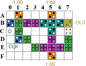
Each cell of proposed QCA D Flip-Flop on their gird position
-
2.
Next, simulation of D flip-flop circuit is performed using QCADesigner tool for each missing cell as well as for each additional cell.
-
3.
The simulation results are observed and evaluated.

Based on simulation results, single missing/additional cells based all possible defects are identified and a list of test vectors are prepared to detect those defects. The results are excelled in Tables 6 and 7 respectively. Table 6 reflects that the output corresponding to missing cell ‘B1’ is ‘1’. Test vector <01> can be used to detect this kind of fault. The correct output of test vector <01> is ‘0’. Thus by comparing the correct output ‘0’ and generated faulty output ‘1’, the fault can be identified.
On the other side, Table 7 shows that the output corresponding to extra cell ‘A0’ is fault free whereas faulty output corresponding to extra cell ‘A4’ is ‘1’, when ‘A4’ is in clock zone 1. Test vector <01> can be used to detect this kind of fault. The correct output of test vector <01> is ‘0’. Thus by comparing the correct output ‘0’ and generated faulty output ‘1’, the fault can be identified. The output corresponding to extra cell ‘A4’ is fault free if ‘A4’ stay in clock zone 2.
The same evaluation technique can be employed to detect all possible defects in the proposed shift register circuit.
Table 6 shows that in case of single missing cell based defect, test vector <01> has (9/15) × 100 = 60 % fault coverage and <11> has (6/15) × 100 = 40 % fault coverage. Thus, the test vector <01, 11> has (60 + 40) % = 100 % fault coverage.
For single additional cell based defect, Table 7 shows that the test vector <01> has (2/7) ×100 = 28.571 % fault coverage and <11> has (5/7) × 100 = 71.428 % fault coverage. In this case, the test vector <01, 11> has (28.571 + 71.428) % = 100 % fault coverage.
Therefore, the test vector <01, 11> provides 100 % fault coverage single missing/additional cell based defects.
4.3 Power dissipation by proposed circuits and existing layouts
In every clock cycle, Hamming distance between input variations is used to estimate the power dissipation of QCA inverter and QCA MV (Liu et al. 2012). For example, if inverter’s input is switched either 0 → 0 or 1 → 1, the Hamming distance is taken as 0 and for either 0 → 1 or 1 → 0 switching; the Hamming distance is considered as 1. The switching in input 000 → 000 to MV, results in Hamming distance of 0 and for 000 → 111 switching, the Hamming distance is taken as 3 (Liu et al. 2012). Each QCA cell has identical power dissipation. In this paper, Hamming distance based approach proposed by Liu et al. (2012) is used in estimation the power dissipation by the layouts. The results are explored in Table 8. The estimation is carried out on temperature T = 2.0 K using different tunneling level. For example, each majority voter of D flip-flop circuit as shown in Fig. 3b has Hamming distance 2. To obtain the maximum power, Hamming distance 1 is considered for all inverters. Then at different tunneling level, the power dissipation calculation of the proposed D flip-flop layout is performed and plotted in Table 8. Similarly, the power dissipation by shift register circuit is estimated and shown in Table 8. The power dissipation at T = 2.0 K by proposed layouts are also shown in Fig. 10.

Power dissipated by each proposed QCA layout
The comparison with existing designs in terms of dissipated energy is shown through Figs. 11and 12. Figure 11 represents the dissipated energy by proposed QCA D flip-flop and previously reported designs and Fig. 12 shows the dissipated energy by proposed QCA SISO shift register and existing ones. It is seen from Fig. 11 that the proposed QCA D flip-flop has slightly lower dissipated energy compare to the designs proposed by Mustafa and Beigh (2014), Ahmad et al. (2014), Goswami et al. (2014), Hashemi and Navi (2012) whereas compare to the designs reported by Lim et al. (2012) and Xiao and Ying (2012) the dissipated energy is very low. Similarly, proposed QCA SISO shift register has lower energy dissipation over previous circuits (Mustafa and Beigh 2014; Ahmad et al. 2014) as shown in Fig. 12. Thus, all the proposed designs have lower energy dissipation than the existing designs.

Power dissipated by proposed QCA D flip-flop and existing designs

Power dissipated by proposed QCA SISO shift register and existing designs
4.4 Stability of proposed QCA design
The stability of the proposed QCA D flip-flop and SISO shift register are demonstrated in this section. The evaluation is performed by simulating those circuits using coherence vector technique of QCA Designer tool (Walus et al. 2004). The simulation is performed in temperature (T) ranging from 1 to 15 K and by considering the relaxation time as 1.00e−015 s (Pudi and Sridharan 2011, 2012). The simulation results are examined to obtain maximum polarization (Pmax), minimum polarization (Pmin) and average polarization (Pavg) for each output cell of the designs. Here, K stands for Kelvin.
4.4.1 Stability of proposed QCA D flip-flop
Pmax, Pmin and Pavg for each output cell of proposed QCA D flip-flop are explored in Table 9. Table 9 shows that Pmax, Pmin and Pavg for output cell ‘OUT’ of QCA D flip-flop as shown in Fig. 3b, remain approximately same in different temperatures. The graphical representation corresponding to Table 10 is shown in Fig. 13. It is seen from Fig. 13 that within temperature 1–12 K, the value of Pmax, Pmin and Pavg have very little changes and QCA D flip-flop has an accurate output. But above 12 K temperature, the value of Pmax and Pmin drops dramatically which results faulty output. Thus the QCA circuit of D flip-flop is stable within temperature 1–12 K. Similar approach can be used to measure the stability of proposed shift register circuit.

Effect of temperature on output polarization of proposed QCA D flip-flop
4.4.2 Stability of proposed QCA shift register
From simulation result, the polarization for each output cell under different temperatures are observed and explored through Table 10. Table 10 demonstrates that Pmax, Pmin and Pavg for each output cell decreases gradually by raising in temperatures. Pmax, Pmin and Pavg for output cell O1, O2, and O3 are plotted in Figs. 14, 15 and 16 respectively. Figure 14 shows that the values of Pmax, Pmin and Pavg are lower if the temperature goes higher. But at any point of temperature level, Pmax, Pmin and Pavg have very little differences in their values. Though the polarization is dropped, up to 12 K temperature the output cell O1 have correct outputs. But above 12 K temperature, the value of Pmax and Pmin are considerably lower which results in faulty output at output cell O1. Similarly, from Figs. 15 and 16 it can also be seen that the values of Pmax, Pmin and Pavg getting lower and within temperature 1–12 K, the polarization is enough to produce correct outputs. Above these temperatures, the polarization is very low and the outputs are incorrect.

Changes in polarization for output cell O1 of proposed QCA shift register

Changes in polarization for output cell O2 of proposed QCA shift register

Changes in polarization for output cell O3 of proposed QCA shift register
Finally the Pavg for all outputs of proposed shift register are plotted in Fig. 17 which shows that there are very small differences between average output polarization i.e., Pavg for the entire output cells O1, O2, and O3. The circuit works efficiently under temperature range 1–12 K. Above 12 K, Pavg for any of the output cell is not well enough to produce correct output and the circuit becomes inefficient.

Changes in average output polarization for output cell O1, O2, and O3 of proposed QCA shift register
4.4.3 Stability of proposed QCA circuits and existing layouts
The comparison of proposed circuits with existing designs in terms of design stability is shown through Figs. 18 and 19. To perform evaluation, the average output polarization (Pavg) for the output cell has been considered.

Pavg of proposed QCA D flip-flop and existing layouts

Pavg of proposed QCA SISO shift register and existing layouts
Figure 18 represents the design stability of proposed QCA D flip-flop and previously reported designs and Fig. 19 shows the design stability of proposed QCA SISO shift register and existing ones. It can be seen from Fig. 18 that the Pavg for proposed QCA D flip-flop is higher at every level of temperatures compare to the designs proposed by Mustafa and Beigh (2014), Ahmad et al. (2014), Goswami et al. (2014), Hashemi and Navi (2012), Lim et al. (2012) and Xiao and Ying (2012). After temperature of 7 K, the Pavg for output cell of existing D flip-flop is dropped drastically, but for proposed D flip-flop Pavg has little changes which is still enough to get correct outputs compare to others. Similarly, it can be seen from Fig. 19 that the Pavg for proposed QCA SISO shift register has higher value at every level of temperatures compare to the designs proposed by Mustafa and Beigh (2014) and Ahmad et al. (2014).
Thus, all the proposed designs are more stable under thermal randomness than the existing designs.
5 Conclusion
This paper outlines an optimized QCA based design of shift register using a new QCA layout of D flip-flop. The designs are achieved in a single layer which provides the simplicity of the circuits. The proposed QCA layouts have less cell count and high device density than existing ones. The dissipated energy by the layouts describes that energy dissipation by all the designs are low. The simulation results establish the accuracy of the layouts when compared to the truth table. The exploration of temperature effect on polarization of each output cell of proposed QCA layouts shows the stability of the circuit. The impact of control input i.e., clock on the designs are explored which describes how the outputs are affected by the clock signal. Besides the defects in proposed QCA layouts are also observed and excelled to obtain error free implementation of the designs. All the designs can be utilized to achieve an advance building block for QCA based counters; linear feedback shift registers at nanoscale level.
References
Ahmad F, Mustafa M, Wani NA, Mir FA (2014) A novel idea of pseudo-code generator in quantum-dot cellular automata (QCA). Int J Simul Multisci Des Optim. doi:10.1051/smdo/2013012
Arjmand MM, Soryani M, Navi K (2013) Coplanar wire crossing in quantum cellular automata using a ternary cell. IET Circuits Devices Syst 7:263–272. doi:10.1049/iet-cds.2012.0366
Das K, De D (2010) Characterization, test and logic synthesis of novel conservative and reversible logic gates for QCA. Int J Nanosci 9:201–214
Das K, De D (2011) Characterisation, applicability and defect analysis for tiles nanostructure of quantum dot cellular automata. Mol Simul 37:210–225
Das JC, De D (2012) Quantum dot cellular automata based cipher text design for nano communication. Int Conf Raddar Commun Comput (ICRCC-12). doi:10.1109/ICRCC.2012.6450583
Das JC, De D (2015a) Reversible binary to grey and grey to binary code converter using QCA. IETE J Res 61:223–229
Das JC, De D (2015b) Reversible Comparator Design using Quantum Dot-Cellular Automata. IETE J Res. doi:10.1080/03772063.2015.1088407
Das JC, De D (2016a) Shannon’s expansion theorem based multiplexer synthesis using QCA. Nanomater Energy 5:53–60. doi:10.1680/jnaen.15.00008
Das JC, De D (2016b) User authentication based on quantum-dot cellular automata using reversible logic for secure nanocommunication. Arab J Sci Eng 41:773–784
Das JC, De D (2016c) Quantum dot-cellular automata based reversible low power parity generator and parity checker design for nanocommunication. Front Inf Technol Electron Eng 17:224–236
Das JC, De D (2016d) novel low power reversible binary incrementer design using quantum-dot cellular automata. Microprocess Microsyst 42:10–23
Das JC, De D (2016e) Optimized design of reversible gates in quantum dot-cellular automata: a review. Rev Theor Sci 4:279–286
Das JC, De D (2016f) Novel low power reversible encoder design using quantum-dot cellular automata. J Nanoelectron Optoelectron 11:450–458
Das JC, De D (2016g) Reversible half-adder design using quantum dot-cellular automata. Quantum Matter 5:(4)476-491
Das K, De D, De M (2012) Competent universal reversible logic gate design for quantum dot cellular automata. WSEAS Trans Circuits Syst 11:401–411
Das K, De D, De M (2013) Realisation of semiconductor ternary quantum dot cellular automata. IET Micro Nano Lett 8:258–263
Das JC, Debnath B, De D (2015) Image steganography using quantum dot cellular automata. Quantum Matter 4:504–517
Das JC, Purkayastha T, De D (2016) Reversible nano-router using QCA for nanocommunication. Nanomater Energy 5:28–42. doi:10.1680/jnaen.15.00012
De D, Bhattacharaya S, Ghatak KP (2013) Quantum dots and quantum cellular automata: recent trends and applications. Nova Science, USA
Debnath B, Das JC, De D (2016a) Reversible logic based image steganography using qca for secure nanocommunication. IET Circuits Devices Syst. doi:10.1049/iet-cds.2015.0245
Debnath B, Das JC, De D (2016b) Correlation and convolution for binary image filter using QCA. Nanomater Energy 5:61–70
Ghosh B, Giridhar M, Nagaraju M, Salimath A (2014a) Ripple carry adder using five input majority gates in quantum dot cellular automata. Quantum Matter 3:495–498
Ghosh B, Agarwal A, Akram MW (2014b) An efficient quantum-dot cellular automata multi-bit adder design using 5-input majority gate. Quantum Matter 3:448–453
Ghosh B, Singh P, Singh SS, Salimath A (2015) Design of 4-bit subtractor using nanotechnology based quantum dot cellular automata. Quantum Matter 4:458–462
Goswami M, Kumar B, Tibrewal H, Mazumdar S (2014) Efficient realization of digital logic circuit using qca multiplexer. In: 2nd International Conference on Business and Information Management (ICBIM). doi:10.1109/ICBIM.2014.6970972
Hashemi S, Navi K (2012) New robust QCA d flip flop and memory structures. Microelectron J 43:929–940
Hashemi S, Navi K (2014) Reversible multiplexer design in quantum-dot cellular automata. Quantum Matter 3:523–528
Kianpour M, Sabbaghi-Nadooshan R (2014) A conventional design and simulation for CLB implementation of an FPGA quantum-dot cellular automata. Microprocess Microsyst 38:1046–1062
Lent CS, Tougaw P (1997) A device architecture for computing with quantum dots. Proceeding IEEE 85:541–557
Lent CS, Liu M, Lu Y (2006) Bennett clocking of quantum dot cellular automata and the limits to binary logic scaling. Nanotechnology 17:4240–4251
Lim LA, Ghazali A, Yan sct, Fat CC (2012) Sequential circuit design using quantum-dot cellular automata (qca). In: IEEE International Conference on Circuits and Systems (ICCAS). doi: 10.1109/ICCircuitsAndSystems.2012.6408320
Liu W, Srivastava S, Lu L, O’Neill M, Swartzlander EE (2012) Are QCA cryptographic circuits resistant to power analysis attack? IEEE Trans Nanotechnol 11:1239–1251
Mustafa M, Beigh MR (2014) Novel linear feedback shift register design in quantum-dot cellular automata. Indian J Pure Appl Phys 52:203–209
Nelson VP, Nagle HT, Irwin JD, Carroll BD (1995) Digital logic circuit analysis and design. Prentice Hall, New Jersey
Pradhan N, De D (2013) Spin transfer torque driven magnetic qca cells. Adv Nanomater Nanotechnol 143:561–569
Pudi V, Sridharan K (2011) Efficient design of a hybrid adder in quantum-dot cellular automata. IEEE Trans Very Large Scale Integr VLSI Syst 19:1535–1548
Pudi V, Sridharan K (2012) Low complexity design of ripple carry and Brent-Kung adders in QCA. IEEE Trans Nanotechnol 11:105–119
Sardinha LH, Costa AMM, Neto OPV, Vieira LFM, Vieira MAM (2013) Nanorouter: a quantum-dot cellular automata design. IEEE J Sel Areas Commun 31:825–834
Sen B, Dutta M, Sikdar BK (2014) Efficient design of parity preserving logic in quantum-dot cellular automata targeting enhanced scalability in testing. Microelectron J 45:239–248
Silva D, Sardinha L, Vieira M, Vieira L, Neto OV (2015) Robust Serial Nano-Communication with QCA. IEEE Trans Nanotechnology 14:464–472
Tehrani MA, Mahmoodi Y, Navi K (2013) Coplanar Architecture for Quantum-Dot Cellular Automata Systolic Array Design. Quantum Matter 2:474–480
Thapliyal H, Ranganathan N (2010) Reversible logic-based concurrently testable latches for molecular QCA. IEEE Trans Nanotechnol 9:62–69
Thapliyal H, Ranganathan N, Kotiyal S (2013) Design of testable reversible sequential circuits. IEEE Trans Very Large Scale Integr VLSI Syst 21:1201–1209
Walus K, Dysart TJ, Jullien GA, Budiman RA (2004) QCADesigner: arapid design and Simulation tool for quantum-dot cellular automata. IEEE Trans Nanotechnol 3:26–31
Xiao XCL, Ying S (2012) Design of dual-edge triggered flip flops based on dot cellular automata. J Zhejiang Univ Sci Comput Electron 13:385–392
Acknowledgments
The authors are grateful to The University Grants Commission, India, for providing with the Grant for accomplishment of the project under the UGC Major Project File No. 41-631/2012(SR).
Author information
Authors and Affiliations
Corresponding author
Rights and permissions
About this article

Cite this article
Das, J.C., De, D. Operational efficiency of novel SISO shift register under thermal randomness in quantum-dot cellular automata design. Microsyst Technol 23, 4155–4168 (2017). https://doi.org/10.1007/s00542-016-3085-y
Received:
Accepted:
Published:
Issue Date:
DOI: https://doi.org/10.1007/s00542-016-3085-y