
Abstract
SOC's have multiple blocks integrated on a single chip, to interact between these blocks, on-chip bus architecture is required. ARM's AMBA (Advanced Microcontroller Bus Architecture) is one of the extensively used on-chip architecture used in the VLSI industry. AHB (Advanced High-Performance Bus) is an AMBA Bus protocol with high-performance, supports multiple masters and multiple slaves and has wider bandwidth; as a result of these features, AHB is generally used in SOC's. Previously, AHB design was verified using either Verilog or system Verilog, where the time spent on verification was more than the time spent on design. A more effective verification methodology, like UVM (Universal Verification Methodology), must be adopted to reduce the average time spent in verification and increase efficiency. An AHB protocol with one master and three slaves is designed in ModelSim using Verilog and verified in QuestaSim using UVM, and a coverage report is generated. QuestaSim and ModelSim are the EDA tools developed by Mentor Graphics for design and verification purposes.
Access provided by Autonomous University of Puebla. Download conference paper PDF
Keywords
1 Introduction
ARM established the open standard bus architecture known as AMBA, which is commonly utilized for on-chip bus systems. The purpose of AMBA is to reduce the design by enabling the usage of replaceable parts inside the SoC. The AMBA includes bus types like APB (Advanced Peripheral Bus), ASB (Advanced System Bus), AHB (Advanced High-performance Bus) and AXI (Advanced Extensible Interface). AHB is designed to address the requirements of high-performance, high bandwidth synthesizable systems [1].
AMBA AHB includes the following characteristics:
-
Burst operation
-
Split transaction
-
Single-cycle bus master handover
-
Single-clock edge operation
-
Non-trivial implementation
-
Supports up to 128-bit bus configuration
Figure 1 shows the AMBA AHB block architecture, which comprises of high-performance devices like on-chip RAM, memory interface and DMA (Direct Memory Access) all connected through an AHB Bus. On the other side, APB (Advanced Peripheral Bus) connects the low bandwidth peripheral devices like UARTs, PIOs, keypads, and timers. A central bridge connects the high-performance bus to the peripheral bus, allowing signals from on-chip devices to be transmitted to peripheral devices.

AMBA AHB block diagram [1]
The work aims to design an AMBA AHB Protocol with one master and three slaves using Verilog HDL and verify the design using UVM.
The paper is structured as follows. Section 2 includes a literature survey on different AMBA AHB verification methodologies. Section 3 describes the design methodology. Section 4 explains the verification methodology. Section 5 describes the simulation results, and Sect. 6 concludes the work with the final analysis.
2 Literature Review
AHB system with three masters and four slaves designed and verified in ModelSim using system Verilog assertions. Where AHB attributes and corner case properties were evaluated, yielding a total coverage report of 80.3% with 20 system Verilog assertions [2].
AHB Single Master Single Slave, Single Master Multi slave, and Multi Master Single Slave were designed and verified in ModelSim using System Verilog [3]. By developing a Verification environment, a comparison was made between Verilog and System Verilog verification methodologies. The comparison revealed that the System Verilog Verification approach produced more accurate results than Verilog.
An AHB protocol was designed using Verilog and verified using system Verilog in QuestaSim [4]. Where the design under test was verified, and coverage report of nearly 65% was generated.
Using a Xilinx simulator, AMBA AHB was designed and verified for simple write and read operations with basic examples using Verilog [5].
AHB system with three masters and four slaves was designed and implemented in Verilog HDL using Xilinx ISE 14.6 [6]. Random combinations of masters and slaves were given to incremental burst operations of four, eight, and sixteen beats.
UVM was used to verify the AHB Protocol, which was built for three masters and four slaves. According to the UVM study conducted, the results obtained were more precise [7].
A single master single slave and multi master multi slave AHB system was designed and verified in ModelSim using UVM (Universal Verification Methodology) [8]. By interfacing STM32 controller, the performance latency of the AHB bus and the baud rate of the USART peripheral were measured which provided 100% functionally corrected output for UVM verification.
To speed up the verification process, a generic and reusable verification environment for SoC buses was developed. When compared to previous methodologies, the recommended methodology reduced verification costs and speeds the verification process [9].
AMBA AHB system was designed with three masters and three slaves, and was verified using both system Verilog and UVM (Universal Verification Methodology) in QuestaSim. Both verification approaches generated coverage reports, with UVM yielding a higher level of coverage than System Verilog [10].
The majority of the relevant work done in the preceding review is on Verilog hardware descriptive language and System Verilog. Along with the design, more work needs to be done in the verification process by using improved verification methodologies.
3 Design Methodology
AMBA AHB architecture with one master and three slaves is shown in Fig. 2, where the master is provided with the bus address, control information and data. The master sends the address to the decoder through the HADDR signal; the decoder broadcasts this address to all of the slaves in the system. The slave with this address will respond to the decoder by turning on its HSELx signal.

AMBA AHB with one master and three slaves
Once the HSELx signal is HIGH, the master will begin transferring data to that slave based on the HTRANS signal, which determines the mode of transfer as shown in Table 1, where there are four data transfer modes IDLE, BUSY, NON-SEQ, and SEQ. The SEQ mode data transfer is dependent on burst operations, like incrementing or Wrapping burst. Once the transfer mode is selected HWRITE signal is used to execute the Write or Read operation.
When the HWRITE signal is HIGH, data is written to the slave, and when the HWRITE signal is LOW, data is read from the slave. After completing the Write or Read, the response, i.e., the HRDATA signal from all slaves, is received and sent to the multiplexer. The multiplexer will multiplex these signals and transmit the HRDATA along with the HRESP signal to master, stating that the data transaction has been completed.
4 Verification Methodology
In VLSI industry large number of chips are being produced every year with a greater number of features. As all features in a chip must be verified before the specified Time to Market, the verification speed has to be increased. This is achieved through the use of a better verification language and a faster verification methodology.
UVM is an IEEE 1800.2 standard since 2017 which was developed by Synopsis in 2010. It is a hybrid of two methodologies: OVM (Open Verification Methodology) and VMM (Verification Methodology Manual). UVM is basically a set of classes defined in the System Verilog language. UVM is a new technology used for verification that is supported by the majority of EDA vendors and extensively accepted in the VLSI industry. UVM minimizes the work of constructing a standard testbench, and also verification components of UVM could be reused across multiple designs.
-
A.
Components of UVM
Figure 3, illustrates a UVM verification environment that includes an interface connected to a DUT with a testbench, agent, generator, driver and monitor forming the subcomponents of the test bench.
Fig. 3 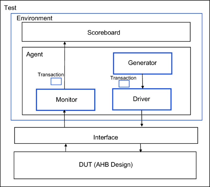
UVM verification environment
-
(1)
Generator: It generates a set of randomized data (where range of random data is specified by the use of assertions) for randomization test or a single data which will be sent to the driver.
-
(2)
Transaction: moves data from generator to driver and also from monitor to scoreboard. Generated by extending UVM_Sequence_item.
-
(3)
Driver: Driver produces stimulus and sends to DUT (Design under Test) through the interface. This is generated by extending UVM_component class.
-
(4)
Agent: The agent consists of the verification components like driver, monitor, and generator which are connected using TLM (Transaction Level Modeling) connections. This is generated by extending UVM_component class.
-
(5)
Interface: It connects driver and monitor to DUT.
-
(6)
Monitor: Receives random or single output from DUT. Derived from UVM_component class.
-
(7)
Environment: Generator, agents, driver and monitor are together placed inside the environment.
-
(8)
DUT (Design Under Test): DUT is the actual design which has to be verified.
-
(9)
Reference Model: This is constructed in case of randomization test to determine whether the random output from DUT is valid.
-
(10)
Scoreboard: It collects the DUT output from the monitor and the output from the reference model and compares both the outputs to check whether DUT outputs are valid.
-
(11)
Testbench: It consists of the test cases. It is generated by UVM_component class.
-
(1)
-
B.
Verification Flow:
The verification can be done in two ways,
-
1.
Directed Test.
-
2.
Randomization Test.
In directed test, single input data is generated and given to the DUT, to obtain respective output. If we have multiple testcases, it is time consuming to check the output for each input data given. So, a set of random data is given as input, and output is determined, this process is called as randomization. As shown in Fig. 4, random data is generated from the generator, this random data is then passed to the driver through transactions, this is called as transaction level modeling (TLM). The driver will send this data along with the instructions to be performed through the interface to the DUT. In DUT, the data is executed and random output is obtained and this is sent to the monitor. To verify the result, a reference model is constructed, which has the same functionality as of the DUT, reference model also takes the random data and produces output. The output from monitor and reference model is given to scoreboard to check whether the results are matching. If it matches, the data has been successfully transferred from slave to master.
Fig. 4 
Verification Flow
-
1.


The scoreboard results contain the following.
-
(1)
Checker: Where assertions are inserted to check whether design is functioning proper or not.
-
(2)
Coverage: Coverage is classified into two categories.
-
Code coverage: The percentage of code that was generated during verification. It can help in locating dead code and false paths, that are not generated for any given combination of inputs.
-
Functional coverage: Indicates the percentage of successful transactions.
-
5 Results and Discussion
-
A.
Decoding:
In the first case, the address given by the master is 32’ h0034, the slave 1 has this address in its memory so the slave 1 is activated by making its HSEL1 signal HIGH as shown in Fig. 5.
Fig. 5 
Decoder Output
In the second case the address 32’h0054 given by the master matches with address present in slave 2, Hence slave 2 is activated by making HSEL2 signal HIGH and Slave 3 will be having the address 32’h0094 in its memory list, so it is activated by making HSEL3 as HIGH.
-
B.
Data Transfer from Master to Slave 1:
When the HWRITE signal goes HIGH, the data 05 h given by the master, is written to the address 34 h present in the memory of slave 1 as shown in Fig. 6. When the HWRITE signal goes LOW, the data which was written into the slave memory is read back which is shown in Fig. 7.
Fig. 6 
Output of AHB write and read
Fig. 7 
Internal Memory of Slave 1
-
C.
Verification Results
The verification results obtained from the scoreboard shown in Fig. 8 show that the output obtained from the DUT and reference model for a random input data is matching, this indicates that the design is generating 100% functionally corrected output.
Fig. 8 
Scoreboard Results
Figure 9, shows the coverage report where Coverage obtained around 96.8%, which shows that most of the test cases are being covered by this method.
Fig. 9 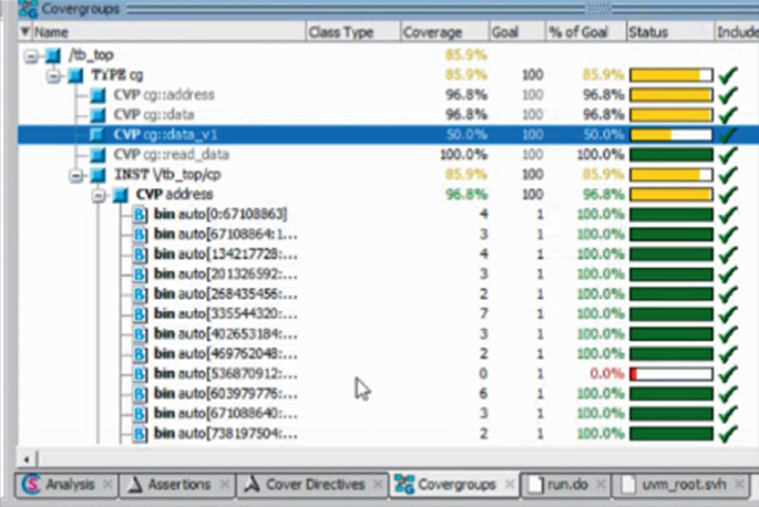
Coverage Results
Figure 9, shows the coverage report where Coverage obtained around 96.8%, which shows that most of the test cases are being covered by this method.


6 Conclusion
This work gives an overview of the AMBA AHB bus protocol, designed with one master and three slaves. The AHB design is implemented in ModelSim tool using Verilog and verified in QuestaSim using Universal Verification Methodology. To verify the exact working and functionality of the design, the entire design is tested under all possible cases in accordance to its specification. The coverage report of 96.8% is obtained from this verification methodology which gives better coverage compared to that of other verification methodologies. In the present work conducted AHB is designed, with one master and three slaves. In future one can design an AHB with 16 masters and 16 slaves and also UVM methodology could be used to verify other buses like APB, AXI, DMA etc.
References
https://developer.arm.com/documentation/ihi0011/a/AMBA-AHB. Accessed 08 April 2022
Gurha P, Khandelwal RR (2016) System verilog assertion based verification of AMBA-AHB. In: International conference on micro-electronics and telecommunication engineering (ICMETE). IEEE
Divya M, Radhakrishna Rao KA (2018) AHB design and verification AMBA 2.0 using system Verilog. Int J Adv Res Ideas Innov Technol 4(3)
Choudhury P, Giridhar P (2019) Design and verification of AMBA AHB. In: 1st international conference on the advanced technology in intelligent control, environment, computing & communication engineering (ICATIECE). IEEE
Shivakumar BR, Deeksha L (2019) Efficient design and implementation of AMBA AHB bus protocol using verilog. In: International Conference on Intelligent Sustainable System (ICISS). IEEE
Bhavana Surya S, Hema C, Shruthi Priya M, Devikarani U, Rathod AS (2021) Design and implementation of multiple master, multi slave interface in AMBA AHB protocol. Int J Res Eng, Sci Manag 4(7)
Ramakrishna MS, Sridevi BS (2018) Verification of advanced high-speed bus in UVM methodology. Int J Res Eng, Sci Manag 1(12)
Deepthi VD (2019) Performance verification of AMBA multi master AHB bus using system Verilog. Int Res J Eng Technol (IRJET) 6(6)
Hussien A, et al (2019) Development of a generic and a reconfigurable UVM-based verification environment for SoC Buses. In: 31st international conference on microelectronics (ICM)
Dilip K, Vijaya Prakash AM (2021) Design and verification of AHB protocol using system verilog and universal verification methodology (UVM). Int J Eng Res Appl 11(7)
Author information
Authors and Affiliations
Corresponding author
Editor information
Editors and Affiliations
Rights and permissions
Copyright information
© 2024 The Author(s), under exclusive license to Springer Nature Singapore Pte Ltd.
About this paper

Cite this paper
Kumari, S., Niranjan, P. (2024). Design and Verification of AMBA AHB Protocol Using UVM. In: Kalya, S., Kulkarni, M., Bhat, S. (eds) Advances in VLSI, Signal Processing, Power Electronics, IoT, Communication and Embedded Systems. VSPICE 2022. Lecture Notes in Electrical Engineering, vol 1062. Springer, Singapore. https://doi.org/10.1007/978-981-99-4444-6_6
Download citation
DOI: https://doi.org/10.1007/978-981-99-4444-6_6
Published:
Publisher Name: Springer, Singapore
Print ISBN: 978-981-99-4443-9
Online ISBN: 978-981-99-4444-6
eBook Packages: EngineeringEngineering (R0)