
Abstract
With the rapid development of clean and renewable energy technology, energy storage devices are more eagerly required. The applicable high temperature superconducting (HTS) materials achieved arouse the superconducting magnetic energy storage (SMES) devices having unique properties to play a substantial role. Superior characteristics have made the SMES technology attractive and a perspective option to practical applications broadly, especially for smart grids (SGs). SMES technology is described and verified including principle, circuit topology, control strategy, and device performance to form a comprehensive understanding of the emerging energy storage technology using the advanced HTS material and associated technology. SMES application is then introduced with the emphasis to develop relevant concepts to suit smart grids (SGs).
Access provided by Autonomous University of Puebla. Download chapter PDF
Keywords
- SMES
- HTS
- HTS inductor
- Smart grid
- Energy storage
- Energy management
- Power inductor charge
- Power electronic device
- Digital control
- Power conditioning system
- Bridge-type chopper
1 Introduction
With the rapid development of modern and new technology industries, the ratio of load sensitivity to power quality is continually rising in proportion, which simply means that the modern society has the urgent need for a higher quality of power supply. On the contrary, the problems of electric power supply caused by the rush of reactive power, power system faults, and operating errors, etc., are becoming more and more serious to modern grids. Adequate action is necessary, such as to compensate reactive power and absorb active power using energy storage systems (ESSs). Energy storage devices and application techniques also play an important role to cooperate with modern green, clean, and renewable energy technology in various fields, which devices have different types and principles, from mechanical to chemical and simple structure to novel material.
High temperature superconducting (HTS) materials and technology have reached the stage for practical applications [1–11] and enabled a potential to realize a practical energy storage device, i.e., HTS superconducting magnetic energy storage—HTS SMES. SMES is in general able to offer fast reaction, high power density, high energy density, light weight, low loss, long life, and environment-friendly operation. Superior characteristics made the SMES attractive and a possible option to practical applications in various fields.
SMESs are introduced with the comparison to various energy storage techniques to identify the emerging technology. Principle, circuit topology, control strategy, device performance, and applications are included to form a comprehensive description and understanding of this emerging technology. The contents consequently include the following sections: (i) Comparisons of various energy storage techniques; (ii) Principal SMES circuits and control techniques; (iii) Experimental prototype and application characteristics; (iv) Development status of worldwide SMES devices; (v) SMES application topologies and performance evaluations in power grids; (vi) Prospective SMES applications in cooperation with electric power smart grids (SGs).
2 Energy Storage Techniques
According to the specific principles, there are three main types of energy storage systems (ESSs): (i) Physical energy storage including pumped hydro storage (PHS), compressed air energy storage (CAES), and flywheel energy storage (FES); (ii) Electromagnetic energy storage including superconducting magnetic energy storage (SMES), super-capacitor energy storage (SCES); (iii) Electrochemical energy storage including lead-acid, lithium-ion, sodium sulfur, and fluid flow battery energy storage, etc. Various types of energy storage devices are summarized in Table 1 as a guideline of technical specifications.
Physical energy storage is a kind of relatively mature and practical energy storage technology, which is limited by topographical and geological conditions to implement. The technology of electrochemical energy storage is evolving fastest so far, of which sodium sulfur battery, fluid flow battery, and lithium-ion battery technologies have made great breakthroughs in energy conversion efficiency, safety, and economy with increasingly industrialized applications. The energy conversion efficiency of sodium sulfur battery can reach 80 % with three times energy density as lead-acid battery with a much longer life cycle.
SMES devices can store the electric energy as electromagnetic energy in the superconducting inductor and release the stored energy if required. Comparing with other energy storage devices, SMES devices have fast response time, high power density, high energy storage efficiency, and long lifetime with little environmental pollution. The current focus on the applied superconducting technology for SMES has been moving to the industrial applications from the laboratory research stage, and the technology has been well verified for practical applications from small to large-scale units.
SMES applications are most commonly associated with the electrical power systems, such as considered for use in SGs recently, meanwhile other applications can also readily be found such as in electric vehicles (EVs), uninterruptible power supplies (UPSs), and power devices with special functions.
3 SMES Circuit and Control Techniques
3.1 Principle and Operation Theory
In general, the SMES-based power apparatuses have the dynamic electric energy exchange between a superconducting coil and an external interface for a power system. With regard to the SMES control, a conventional chopper having two power switches and two power diodes is mostly applied to link the HTS coil to the DC bus and to achieve the bidirectional power exchange for managing the generated power of distributed generators (DGs) or maintaining the uninterruptible power of critical electric equipment. As shown in Fig. 1, a typical power conditioning system (PCS) with voltage source converter (VSC), it has three main operation states, i.e., energy charge state, energy storage state, and energy discharge state. The HTS coil is charged by a DC power source through the power switches S 1, S 2, then stores its magnetic energy through the power switch S 2 and the power diode D 1, and finally discharges its stored energy to the external load through the power diodes D 1 and D 2, respectively. Figure 2 shows the operation principles of the conventional chopper.

Circuit topology of a typical power conditioning system

Operation principles of the conventional chopper. a Energy charge state; b Energy storage state; c Energy discharge state
According to the state-of-the-art power electronic technologies [12], the applicable voltage rating of the insulated gate bipolar translators (IGBTs) is between 0.5 and 6.5 kV. Since the most SMES devices in the world are developed for kV-class power distribution applications [13], IGBTs are normally applied to form a conventional chopper. Even when the operation voltage across the HTS coils drops to 750 V in the ongoing 2.4 GJ SMES project [14], IGBTs still have the advantages over MOSFETs. However, if the applicable voltage ratings are below 500 V, the metal oxide semiconductor field effect transistors (MOSFETs) are more suitable to achieve high-efficiency and high power energy conversions for various end-users’ applications such as EVs [15] and UPSs [16]. Meanwhile, the turn-on resistances in the commercial low-voltage MOSFETs have already been reduced to Milliohm level or below, which results in much lower consumed power than that in the power diodes.
Recently, new focuses of low-voltage SMES applications have been formed for various power end-users. The rapid developments of hydrogen-powered fuel cell vehicles (FCVs) make it available to cool the HTS or MgB2 coils by fully making use of the onboard liquid hydrogen (LH2). The SMES technology has been technically verified [17, 18] to improve the fast repeated charge–discharge performance for regenerative braking. Meanwhile, some low-voltage direct-current (LVDC) power transmission systems have been proposed and studied to connect with various DC output type distributed generators (DGs) [19] such as photovoltaic (PV) cells and fuel cells (FCs), and to supply the electric loads in the commercial and residential buildings [20]. The superconducting DC cable with nearly zero energy loss has been applied to achieve high power and long-distance power transmission, with an additional SMES device introduced to enhance the whole power transfer capacity and stability [21, 22]. In the above low-voltage applications, several considerable benefits from the SMES technology can be derived to improve the power quality for the end-user, to achieve high-efficiency operation for energy saving, and to lower the capital cost of the SMES device. Therefore, beside the current large-scale SMES applications for power transmission and distribution, small-scale SMES devices also have very promising application prospects for use in the power end-user systems.
Consequently, a new bridge-type chopper using MOSFETs is proposed [23] and analyzed to reduce the energy loss for low-voltage applications. The circuit topology of the bridge-type chopper is shown in Fig. 3. It mainly consists of four low-loss power diodes, i.e., MOSFETs S 1–S 4 paralleled with their reverse diodes D 1–D 4, and a DC-link capacitor C paralleled to the load R. Like the conventional chopper, it also has the same three main operation states. In addition, owning to the inevitable turn-on and turn-off delayed time of a practical power switch, two transient operation states are necessary to avoid potential short circuits of the DC power supply and DC-link capacitor.

Topology of the bridge-type chopper
When the bridge-type chopper operates at energy charge state, the HTS coil L is charged by a DC power supply U through S 1 and S 3, as shown in Fig. 4. The circuit voltage equation can be expressed by

Energy charge state of the bridge-type chopper
where I L (t), transient current through the HTS coil; R L , lossy resistance from the connection junctions and current leads in the HTS coil; R s , turn-on resistance of the MOSFET unit.
When I L (t) reaches its reference value, the bridge-type chopper comes into the energy storage state. As shown in Fig. 5, the HTS coil L will be formed as a transient energy storage circuit through D 2 and S 3 during the first transient storage time period 0–T i , and then formed as a steady energy storage circuit through S 2 and S 3 after T i . T i is the time duration of a transient operation state, which is larger than both the turn-on and turn-off time durations of a MOSFET. The circuit voltage equations in the above two energy storage states can be expressed by

Energy storage state of the bridge-type chopper. a Transient storage state; b Steady storage state
The circuit current equation in the load side can be expressed by
where U R (t), transient voltage across the load R; C, snubber capacitance of the DC-link capacitor.
When U R (t) is below its reference value, the bridge-type chopper comes into the energy discharge state. As shown in Fig. 6, the HTS coil L will exist as part of a transient energy discharge circuit through S 2 and D 4 during the first transient discharge time period 0–T i, and then exists as part of a steady energy discharge circuit through S 2 and S 4 after T i. The circuit voltage equations in the above two energy discharge states can be expressed by

Energy discharge state of the bridge-type chopper. a Transient discharge state; b Steady discharge state
The circuit current equation in the load side can be expressed by
3.2 Principle of Control and Protection
Defining the turn-on or turn-off status of a power switch as “1” or “0,” the system operation states of the bridge-type and conventional choppers can be digitalized, as shown in Table 2. Besides the three steady operation states of charge state, storage state, and discharge state in the conventional chopper, the bridge-type one has two more transient operation states to avoid the short circuits of the power source and DC-link capacitor, as shown in Fig. 7. In practice, the HTS coil is normally controlled to carry out the bidirectional energy exchanges with the external system. A digital control method is consequently introduced to achieve the controlled energy charge, storage, and discharge processes. In normal operation, when the load resistor is operated at a power swell state, the real-time operation state of the two choppers will be converted between charge state and storage state alternately to absorb the surplus power. Similarly, when the load resistor is operated at a power sag state, the real-time operation state will be converted between discharge state and storage state alternately to compensate the shortfall power. The above two dynamic processes can be defined as “charge-storage mode” and “discharge-storage mode.”

Digital state diagram of the two choppers. a Bridge-type chopper; b Conventional chopper
A concept of maximum permissible relative voltage error λ m (t) is introduced to divide the three main operation states, and can be expressed by
where U max(t) and U r (t) are the maximum overshoot voltage and rated voltage across the DC-link capacitor and resistive load; U r is reference voltage.
Thus the three main operation states are described as follows: (i) When the instantaneous relative voltage error λ(t) meets the condition of −λ m (t) ≤ λ(t) ≤ λ m (t), the chopper is operated at energy storage state; (ii) When λ(t) meets the condition of λ(t) < −λ m(t), the chopper is operated at energy discharge state; (iii) When λ(t) meets the condition of λ(t) > λ m (t), the chopper is operated at energy charge state. During the dynamic energy exchange processes, the chopper will be operated at a charge-storage mode or a discharge-storage mode when I L (t) is larger than the shortfall current I sh(t) or surplus current I su(t). I Lr is the rated current through the HTS coil. The whole operation flow diagram of the digital control method developed is shown in Fig. 8.

Operation flow diagram of the digital control method
In addition, a fault detection and protection module is particularly required to avoid the potential risks like short circuit, overcurrent, and overvoltage. Four main fault operations are described as follows: (i) I L (t) exceeds its maximum allowable value I m ; (ii) U R (t) exceeds its maximum allowable value U m ; (iii) The current input signals s in of the module do not belong to the sequences ss of all the digital control signals in Fig. 7; (iv) The value of s in xor s out does not belong to the sequences s xor of “0001,” “0010,” “0100,” and “1000,” If a fault operation is detected, the current operation state should be converted into storage state immediately, as shown in Fig. 9. s out is the last output signals of the module. ss ch is the sequences of the digital control signals in the charge-storage mode. T d is an inevitable time delay in a practical digital control system.

Operation flow diagram of fault detection and protection
3.3 Principle and Implementation of a Novel Digital Prediction Control Method
To achieve high-performance applications and avoid operation risks caused by various real-time statuses such as critical current, AC loss, and electromagnetic force, superconducting magnets generally need to operate precisely during the charge, storage, and discharge processes. However, owning to the existence of an inevitable time delay consisting of the sampling time of the controlled variables, computing time of the digital control chip, and implementing time of the controlled objects [24, 25], the digital control signals from a practical digital system usually lag behind the changes of the controlled variables, which results in some undesired overshoots.
A new digital prediction control method is proposed to limit the controlled variables into their desired reference ripple ranges. The principle is to predict the instantaneous time t r when the practical controlled variable, e.g., U R (t), reaches its reference value and to output the corresponding digital control signals at t r − T d in advance. The whole prediction control process during the discharge-storage mode is shown in Fig. 10 and particularly presented as follows.

The whole prediction control process of the proposed method
3.3.1 The Estimations of the Initial Current and Voltage Values by Linear Extrapolation Method
Assume that the digital control chip outputs the state-switching signals at a certain time t 1, and the time interval from the nearest sampling time to t 1 is T 2, thus the bridge-type chopper will change its operation state at t 1 + T d . However, I L (t) and U R (t) at t 1 + T d are very difficult to be sampled precisely because the practical sampling time period T s cannot be infinitely small. The number of the sampled data p can be obtained by rounding (T 2 + T d )/T s , and the nearest sampling time to t 1 + T d is T 3 = T 2 + T d − p × (T 2 + T d )/T s , thus the initial voltage U 0 across the load at t 1 + T d can be estimated by
where U 11 and U 22 are the sampled voltage values at T 3 − T s and T 3, respectively. The initial current I 0 through the superconducting magnet at t 1 + T d can be estimated by the similar method.
3.3.2 The Computations of the Critical Voltage Values by Chopper Circuit Equations
Applying the estimated initial current and voltage values (I 0, U 0) into (6) and (7), U R (t) during the current operation state can be computed and predicted. Assume that the permissible voltage ripple range is from U r − U rip to U r + U rip, thus the time T rip, when U R (t) = U r + U rip, can be computed by (6) and (7) in the energy discharge state, and the digital control chip should output the state-switching signals at T rip − T d. As shown in Fig. 11, U R (t) at T rip − T d − T s and T rip – T d are computed and defined as two critical voltage values (U 33, U 44) for state-switching judgement.

The computations of U 33, U 44 by chopper circuit equations
3.3.3 The Estimation of the State-Switching Time by Linear Interpolation Method
The sampled U R (t) is used to compare with U 33 and U 44, and to predict the precise state-switching time. When U 33 ≤ U R (t) ≤ U 44, the time interval T sw from the sampled time to T rip − T d can be estimated by
Thus the digital control chip outputs the state-switching signals after T sw, and finally makes the bridge-type chopper convert into storage state when U R (t) = U r + U rip.
Figure 12 shows the voltage curve (blue line) across the external load and its corresponding digital control signal “S 4” for the switch S 4 by using the conventional and improved methods. If the turn-on and turn-off time delay of a switch is ignored, the practical state-switching control signal (red dotted line) corresponds to the voltage overshoots. However, if the improved method is applied, the digital control chip will output the state-switching control signal (green line) 0.05 ms before the time when U R (t) reaches 9.95 or 10.05 V, thus U R (t) can be precisely limited from 9.95 to 10.05 V.

U R (t) and “S 4” during the discharge-storage mode (U r = 10 V, U rip = 0.05 V, T d = 0.05 ms). a with the conventional method; b with the improved method
4 Experimental Verification and Characteristics
4.1 Experimental Prototype Design
Figure 13 shows the schematic diagram of a unified energy exchange prototype for SMES study. Four Infineon N-channel MOSFETs with ultra-low turn-on resistance (R s ≈ 0.65 mΩ, under 100 A operation current) are introduced to develop the bridge-type chopper, with the power lines among the four MOSFETs formed by silvered copper bars. S 1, S 2, and, two reverse power diodes of S 2 and S 4 can be also used to form a conventional chopper for experimental tests and comparisons. The parameters of the reverse diode are U d ≈ 0.65 V and R d ≈ 2.3 mΩ. Thirty-two Nichicon conductive polymer aluminum solid electrolytic capacitors with ultra-low equivalent series resistance (R esr ≈ 11 mΩ) are connected in parallel to serve as the DC-link capacitor. The power-line resistor R line is arbitrarily combined by three 0.5 Ω resistors. The power-load resistor R load has three parallel resistor branches of R 1, R 2, and R 3. The available resistors in each branch are one 1-Ω resistor and two 2-Ω resistors, and can be controlled to connect or disconnect to the power-line resistor by a MOSFET.

The schematic diagram of the unified energy exchange prototype
The HTS coil used in the experiments is a 0.2 H HTS coil wound with Bi-2223 tapes. It consists of three solenoids in series for reducing the internal connections inside the HTS coil, and is operated under liquid nitrogen (LN2) condition. The specifications of the HTS coil are shown in Table 3.
Based on the referred switching control requirements, a Micro-programmed Control Unit (MCU) was employed to build the digital control module of the system. As shown in Fig. 14, load voltage U R (t) and coil current I L (t) are sampled back to the MCU to determine the next output signals; the drive circuit mainly consisting of light coupling isolation devices to ensure the output signal from the MCU can adequately drive the MOSFETs. The protection circuit is built based on CPLD. The protection function includes two parts: one is illegal logic protection for signals from the MCU; the other is overcurrent and overvoltage protection.

A digital control module of the system
The main operation processes are described as follows: (i) Apply the power source to charge the DC-link capacitor through the power-line resistor, U R (t) increases gradually to the output voltage U of the power source; (ii) Close S 1, S 3 and S 5, the HTS coil is charged and I L (t) increases gradually to its preset initial value I 0; (iii) Open S 1, and then close S 2, the chopper is operated in the storage state; (iv) Open S 5, and then close one, two or three branched switches of S 6, S 7, and S 8, the corresponding branched resistors are connected to the power source through the power-line resistor; (v) The MCU and CPLD joint measurement and control unit are to implement the online voltage monitoring of U R (t) and further to change the next operation state of the chopper accordingly.
4.2 Experimental Verifications and Comparisons
4.2.1 Analysis on the Energy Absorption Characteristics
In the experiment, a DC power source U = 15 V is first applied to the power-line resistor R line = 0.5 Ω and power-load resistor R load = 0.25 Ω. The power-load resistor is formed by three parallel branches of R 1 = R 2 = 1 Ω, R 3 = 0.5 Ω. Each branched resistor is operated at its rated voltage U r = 5 V. Assume that R 2 and R 3 are disconnected from the time t = 0 s to t = 6 s, U R (t) will increase quickly to 10 V without SMES, and thus the remaining branched resistor R 1 is operated at a voltage swell state. If the SMES is applied, the 0.2 H HTS coil should be controlled to absorb the mean surplus power P su = 75 W and the mean surplus current I su = 15 A.
Figure 15 shows the measured results of I L (t) and U R (t) during the whole energy absorption processes, which can be divided into three different segments. The first one is an incomplete absorption segment when I L (t) < 15 A, both the bridge-type and conventional choppers will be operated at a charge state until U R (t) drops to 5 V again. The second one is a complete absorption segment when 15 A ≤ I L (t) < 60 A, the two choppers are operated at a charge-storage mode to maintain U R (t) around 5 V. Once I L (t) reaches its rated operation current I Lr = 60 A, the third process enters into an incomplete absorption segment, and the surplus power cannot be absorbed completely. If an additional persistent current switch [26, 27] with nearly zero resistance is applied to connect with the HTS coil when its operation current reaches its rated value, the third process will be a zero absorption segment.

The measured results of I L (t) and U R (t) during the whole energy absorption processes. a I L (t) versus t; (b) U R (t) versus t
Figure 16 shows the measured results of U R (t) in the first incomplete absorption segment when I L (t) < 15 A. If I 0 < 15 A, at the time t = 0, U R (t) will increase quickly to a peak voltage U m , and then decreases gradually to 5 V after an incomplete absorption time duration T m . Since the same MOSFETs S1 and S3 are used, both the bridge-type and conventional choppers have the same operation parameter in the incomplete absorption process.

The measured results of U R (t) when I 0 < 15 A
In the following complete absorption segment, the maximum absorption time duration T abs to absorb such a 75 W surplus power in the bridge-type chopper is shorter than that in the conventional one. As shown in Fig. 17, the measured results match well with the calculated results from the theoretical model, and the measured T abs values in the bridge-type chopper are in very close proximity to the ideal values, so the bridge-type chopper has a higher energy utilization efficiency η than the conventional one. When I 0 = 15 A, the measured η values are about 91.5 and 61.9 % for the bridge-type and conventional chopper, respectively. However, for a practical SMES system with a determined I Lr, the conventional chopper seems to be more suitable to achieve a longer T abs to satisfy with the external absorption demands.

The measured and calculated results of T abs versus I 0
4.2.2 Analysis on the Energy Compensation Characteristics
In the experiment, a DC power source U = 15 V is first applied to the power-line resistor R line = 0.5 Ω and power-load resistor R load = R 1 = 1 Ω. The branched resistor R 1 is operated at its rated voltage U r = 10 V. Assume that R 2 and R 3 are connected from the time t = 0 to 1.8 s, U R (t) will decrease quickly to 5 V without SMES, and thus the three branched resistors are operated at a voltage sag state. If the SMES is applied, the 0.2 H HTS coil should be controlled to compensate the mean shortfall power P sh = 300 W and mean shortfall current I sh = 30 A.
Figure 18 shows the measured results of I L (t) and U R (t) during the whole energy compensation processes, which can also be divided into three different segments. The first one is a complete compensation segment when I L (t) ≥ 30 A, both the bridge-type and conventional choppers are operated at a discharge-storage mode to maintain U R (t) around 10 V until I L (t) drops to 30 A. The second one is an incomplete compensation segment when I L (t) < 30 A, the two choppers are operated at a discharge state to compensate a decreasing power. Once I L (t) drops to zero, the operation state of the two choppers should be converted into storage state to avoid the occurrence of reverse charge, and thus the third process enters into a zero compensation segment.

The measured results of I L (t) and U R (t) during the whole energy compensation processes. a I L (t) versus t; b U R (t) versus t
In the complete compensation segment, the maximum compensation time duration T com to compensate such a 300 W shortfall power in the bridge-type chopper is longer than that in the conventional one, as shown in Fig. 19. When I 0 = 60 A, the measured η values are about 97.1 and 83.2 % for the bridge-type and conventional chopper, respectively. Furthermore, if several MOSFETs are applied in parallel to serve as a power switch, both T com and η can be further enlarged to approximately equal to that in an ideal chopper. However, the method to use several parallel power diodes cannot enlarge T com and η effectively because of the inevitable power loss from the stationary voltage drop in the conventional chopper. Therefore, the bridge-type chopper has the potential to replace the conventional one in some low-voltage power applications like an SMES-based dynamic braking drive system of an AC motor [28]. Both the absorption and compensation efficiencies for kinetic energy of the motor will be much improved. The bridge-type chopper can also be directly applied to connect the HTS coil with DC bus in a micro grid (MG) [19]. Besides the significant improvement of practical energy exchange efficiency, the practical response time to absorb or compensate the electric energy will be reduced to microsecond level, which is very beneficial to enhance the power quality with the end-user.

The measured and calculated results of T com versus I 0
Figure 20 shows the measured results of U R (t) in the incomplete compensation segment when I 0 ≤ 30 A. If I 0 < 30 A, at the time t = 0 s, U R (t) will decrease quickly to a inflected voltage U c , and then decreases gradually to 0 V after an incomplete compensation time duration T c . The measured U c values in the two choppers are similar, however, the bridge-type chopper will achieve a longer T c than the conventional one.

The measured results of U R (t) when I 0 ≤ 30 A
4.2.3 Analysis on the Energy Exchange Characteristics
The energy absorption and compensation processes of the energy exchange prototype have been presented independently in Sects. 4.2.1 and 4.2.2. To further discuss the dynamic energy exchange characteristics, one branch and three branches of R 1 = R 2 = R 3 = 1 Ω are connected with the power-line resistor R line = 0.5 Ω to achieve a power swell state and a power sag state, respectively. As shown in Fig. 21, the 0.2 H HTS coil should be controlled to absorb the mean surplus power P su = 100 W until the time when t = 5 s in the bridge-type chopper or t = 6 s in the conventional chopper, and then to compensate the mean shortfall power P sh = 100 W until the time when t = 9 s. The whole energy exchange processes can be divided into six different segments: (i) Incomplete absorption segment when I L (t) < 10 A; (ii) Complete absorption segment when 10 A ≤ I L (t) < 60 A; (iii) Incomplete absorption segment when I L (t) ≈ 60 A; (iv) Complete compensation segment when I L (t) ≥ 10 A; (v) Incomplete compensation segment when 0 A < I L (t) < 10 A; (vi) Zero compensation segment when I L (t) = 0 A.

The measured results of I L (t) and U R (t) during the whole energy exchange processes. a I L (t) versus t; b U R (t) versus t
Similarly, the dynamic energy exchange characteristics in all the energy absorption and compensation segments can be fully obtained by integrating the theoretical and experimental studies in Sects. 4.2.1 and 4.2.2. The available parameters and data curves mainly include: (i) U m , T m , U c , and T c in the incomplete absorption and compensation segments when I L (t) < 10 A; (ii) T abs and T com in the complete absorption and compensation segments when 10 A ≤ I L (t) ≤ 60 A; (iii) I L (t) and U R (t) at an arbitrary time; (iv) Transient voltage, current, consumed power curves of the power-line resistor and power electronic elements.
The above operation parameters and relevant relations probably follow several power and linear functions as follows: (i) Incomplete absorption segment, U m = −0.306I 0 + 9.514, T m = −0.027I 0 + 0.435; (ii) Complete absorption segment, T abs = −1.333 × (I 0)2 × 10⁻³ + 4.8 in the ideal chopper, T abs = −5.515 × (I 0)2 × 10−2.234 + 5.157 in the bridge-type chopper, T abs = −4.165 × (I 0)2.945 × 10⁻⁵ + 7.285 in the conventional chopper; (iii) Complete compensation segment, T com = 3.333 × (I 0)2 × 10⁻⁴ − 0.3 in the ideal chopper, T com = 3.928 × (I 0)1.957 × 10⁻⁴ − 0.3054 in the bridge-type chopper, T com = 6.336 × (I 0)1.813 × 10⁻⁴ − 0.3054 in the conventional chopper; (iv) Incomplete compensation segment, U c = 0.171I 0 + 4.853, T c = 0.024I 0 + 0.125 in the bridge-type chopper, T c = 0.021I 0 + 0.08 in the conventional chopper. The fitted linear and power functions have the potential to apply in practical SMES design and optimization for use in different power system applications. The proposed system also provides a feasible method to build a simple and economical test apparatus for the experimental evaluations of an SMES device before its practical applications.
Based the above theoretical and experimental results obtained, conclusions can be made as follows: As compared to the conventional chopper, the bridge-type one has higher energy utilization efficiency in various power end-user applications such as EVs, UPSs, DGs, and LVDC systems. What’s more, the energy utilization efficiency can be further improved by introducing the MOSFETs with lower applicable voltage level or adopting the multi MOSFET in parallel connection method. However, similar methods cannot improve the efficiency significantly in the conventional chopper because of the inevitable power loss from the stationary voltage drop across the two power diodes. If one simply considers the practical energy exchange effects to satisfy with the external demands, a better application scheme is to use the charge-storage mode of the conventional chopper during the energy absorption process, and to use the discharge-storage mode of the bridge-type chopper during the energy compensation process. The scheme will integrate the advantages of the two choppers for achieving very long absorption and compensation time durations.
5 Development Status of Worldwide SMES Devices
In recent years, with the development of superconducting materials, especially HTS materials with promising strong-current applications in large-scale magnets, various SMES devices have been fabricated and tested for practical power grids. The main LTS and HTS SMES devices worldwide are summarized in Table 4 and Table 5 [29–31].
Serious interests in SMES began in the early 1960s as reliable low-temperature superconductors (LTSs) became available. The practical feasibility of the SMES concept has been demonstrated with the world’s first commercial 30 MJ NbTi SMES unit [32] used on the Pacific Intertie transmission line in the early 1980s. At this point in time, the LTS SMES technology is relatively mature and reliable; USA has developed several large-scale SMES devices, e.g., 30 MJ SMES in Los Alamos National Laboratory (LANL) [32], 100 MJ SMES in University of Florida [33], and has already achieved the primary process of commercialization. Other countries in the world have also developed several MJ-class LTS SMES devices, e.g., Chubu Electric Power Co. in Japan—7.34 MJ SMES [34], Chinese Academy of Sciences in China—2 MJ SMES [35], Korean Electric Research Institute in Korea—3 MJ SMES [36], Ansaldo Ricerche spa in Italy—2.6 MJ SMES [37], etc. The power system applications of the current LTS SMES devices include damping low-frequency oscillation in the interconnected grid, maintaining power system stability, compensating voltage dip, protecting critical load, etc. However, the high refrigeration loads, which is required to keep the LTS materials at 4.2 K, made the LTS SMES uneconomical to practically operate. For LTS SMES further developments, the high refrigeration cost remains a significant barrier.
Immediately following the discovery of HTS materials in 1986, several studies looked into the feasibility of HTS SMES. Due to the anisotropy of 1G HTS tapes and immature HTS high-field magnet technology, the number of the worldwide HTS SMES devices is relatively few by comparison to LTS SMES devices, and the achieved capacities are limited to MJ-class, e.g., Chubu Electric Power Co. in Japan—1 MJ SMES [38], Chinese Academy of Sciences in China—1 MJ SMES [39], CNRS-CRTBT-LEG in France—0.8 MJ SMES [40], Korean Electric Research Institute in Korea—0.6 MJ SMES [41], etc. The HTS magnets in the above MJ-class HTS SMES devices are fabricated by 1G BSCCO tapes (Bi2212 or Bi2223), which have been considered as transitional materials for studying HTS magnet technology. With the continued development of HTS wires, the second generation (2G) YBCO tapes became more feasible, and their outstanding high-field properties make large-scale HTS SMES available, i.e., 2.4 GJ YBCO SMES [14]. Recently a new promising SMES technology based on MgB2 tapes has been proposed to combine with liquid hydrogen (LH2) for developing very compact hybrid ESSs, i.e., 48 GJ MgB2 LIQHYSMES [42].
The continuous progresses of HTS materials and SMES devices have formed the firm base for the SMES developments and applications ranging from small to large scales in distribution to transmission power systems and future SGs. In addition, the suitable reduction of capital cost for SMES devices with the price reduction of HTS conductors (BSCCO tapes for about 35 $/kA·m or below, YBCO tapes for about 15 $/kA·m or below), large-scale SMES devices will become economically available, and will play an important role in future SGs.
6 SMES Application Topologies and Performance Evaluations
With the development of micro grids (MGs) and smart grids (SGs), it is expected that combination of centralized power generation and distributed power generation for developing modern resource-saving and environment-friendly power systems will occur in future. The ultimate purpose is to satisfy the increased power quality requirements from modern power consumers. Fast response, high efficiency, large-scale energy storage systems (ESSs) play an important role for smart regulation and control in flexible AC transmission systems (FACTS) for power transmission, distributed flexible AC transmission systems (DFACTS) for power distribution, and widespread renewable energy sources (RESs) penetration and replacement of the current fossil-fuel power generation. This section summarizes the application topologies and evaluates the high-performance SMES devices for power grid applications.
6.1 Basic VSC and CSC Application Topologies
6.1.1 VSC-Based SMES
Figure 22, as an example, shows the basic configuration of a VSC-based SMES unit [57], which consists of a Wye-Delta transformer, a six-pulse pulse width modulation (PWM) rectifier/inverter using insulated gate bipolar transistor (IGBT), a two-quadrant DC–DC chopper using IGBT, and a superconducting coil or inductor. The PWM converter and the DC–DC chopper are linked by a DC-link capacitor.

Basic configuration of VSC-based SMES system
The PWM VSC provides a power electronic interface between the AC power system and the superconducting coil. The control system of the VSC is shown in Fig. 23. The proportional-integral (PI) controllers determine the reference d- and q-axis currents by using the difference between the DC-link voltage E DC and reference value E DC_ref, and the difference between terminal voltage V G and reference value V G_ref, respectively. The reference signal for VSC is determined by converting d- and q-axis voltages which are determined by the difference between reference d–q axes currents and their detected values. The PWM signal is generated for IGBT switching by comparing the reference signal which is converted to a three-phase sinusoidal wave with the triangular carrier signal. The DC voltage across the capacitor is kept constant throughout by the six-pulse PWM converter.

Control system of the VSC
The superconducting coil is charged or discharged by a two-quadrant DC–DC chopper. The DC–DC chopper is controlled to supply positive (IGBT is turned ON) or negative (IGBT is turned OFF) voltage V sm to the SMES coil and then the stored energy can be charged or discharged. Therefore, the superconducting coil is charged or discharged by adjusting the average voltage V sm_av across the coil which is determined by the duty cycle of the two-quadrant DC–DC chopper. When the duty cycle is larger than 0.5 or less than 0.5, the stored energy of the coil is either charging or discharging, respectively. In order to generate the PWM gate signals for the IGBT of the chopper, the reference signal is compared with the triangular signal.
6.1.2 CSC-Based SMES
Figure 24, as an example, shows the basic configuration of a current source converter-based (CSC-based) SMES unit. The DC side of CSC is directly connected with the superconducting coil, and its AC side is connected to the power line. A bank of capacitors connected to a CSC input terminal is utilized to buffer the energy stored in line inductances in the process of commutating direction of AC line current. Furthermore, the capacitors can filter the high-order harmonics of the AC line current. In the CSC, through regulating the trigger signals of the switching devices, the current in the superconducting coil can be modulated to generate controllable three-phase PWM current at the AC side. As the SMES system is inherently a current system, the transfer of both active and reactive powers between the CSC and power network is very fast.

SMES system with a CSC
In case of a 12-pulse CSC-based SMES, to improve the total harmonics distortion (THD) of the ac source currents, an optimal PWM switching strategy is used to minimize the 5th, 7th, 11th, and 13th harmonics. It has been proved that the 5th, 7th, 11th, and 13th harmonics can be minimized to zero with the modulation index ranging from 0.2 to 1. Compared to a 6-pulse CSC, the 12-pulse CSC has smaller voltage ripples on the dc side, which means a further reduction of the ac losses in the SMES coil.
For magnet training, a DC current (I d ) control algorithm is applied. The block diagram is shown in Fig. 25, where I dref is the reference value of I d , PI is a proportional-integral regulator, L is the inductance of the SMES coil, R d is the resistance in the DC circuit, and V d is the DC voltage. With the phase angle α being fixed to zero, the DC voltage is proportional to the modulation index M, which determines the charging rate.

Block diagram of the DC current control algorithm
6.2 Integrated Application Topologies in Power Grids
6.2.1 Application Topologies in Distributed Generators and Micro Grids
To reach widespread RESs penetration and replacement of the current fossil-fuel power generation, an innovative concept of micro grid (MG), which integrates several DGs and distributed ESSs, has been proposed to achieve large power quality improvements and comprehensive utilizations of various local DGs. A typical MG system with an SMES is shown in Fig. 26 [30, 31]. The generated power of the solar power system, wind power system, and hydro power system are gathered in the DC bus through several power conversions. The SMES system carries out dynamic power exchange with the DC bus to maintain the power stabilization in DC bus. The MG system can be applied as a power supply for independent loads and grid loads.

A typical MG system with SMES
There are three main technical advantages in the MG system with an SMES: (i) SMES with rapid response characteristics (ms level) can, such as voltage interrupt, instantaneous voltage dip, etc.; (ii) SMES with very large power output characteristics (MW level) can provide enough compensation power for DC bus; (iii) SMES with very high energy storage efficiency characteristics can improve the operation efficiency in the whole MG system.
6.2.2 Application Topologies in Transmission and Distribution Systems
To solve different power quality problems, e.g., voltage sag, voltage swells, voltage fluctuation, interruptions, harmonics, etc., various power conversions, compensation, and control devices have been introduced to regulate and control the transmission and distribution systems. The main solutions for various power quality problems include FACTS for the power transmission side and DFACTS for the power distribution side. Three basic FACTS and DFACTS devices, i.e., series-type static synchronous series compensator—SSSC, static synchronous compensator—STATCOM, unified power flow controller—UPFC, with an SMES unit in the device, are shown in Fig. 27. The integrated application schemes of SMES-FACTS/DFACTS in power transmission line (TL) and distribution line (DL) are shown in Fig. 28.

Three typical FACTS/DFACTS with SMES. a SMES-SSSC; b SMES-STATCOM; c SMES-UPFC

The integrated application schemes of SMES-FACTS/DFACTS
6.2.3 Integrated Application Topologies in Smart Grids
Based on the above discussions, the prospect of SMES in future SG is proposed in Fig. 29. In addition to the traditional power generation plants including hydro power plants, thermal power plants, and nuclear power plants, various MGs or DGs using RESs will be widely installed in future SGs. With the dynamic power exchange and regulation from SMES or hybrid ESSs, MGs or DGs can be directly connected to the main power transmission and distribution lines (DLs). SMES-based FACTS and DFACTS devices can be further applied to carry out the whole power flow control for reaching the increasing power demands from modern power consumers (PCs). The real-time signals in the whole SG will be transmitted to the smart control center for data processing and finally achieving the integrated power management and control of FACTS, DFACTS, and MGs. As an auxiliary power management technology, SMES-based UPS installed in the power terminals will guarantee the power quality for various PCs.

The integrated application prospects of SMES in future smart grid
6.3 Applications of SMES in Power Grids
The application topologies and advantages of SMES for MGs, transmission and distribution systems are described in this section. The application scheme of hybrid ESSs with distributed SMES devices are proposed and discussed to combine the advantages from SMES devices and other conventional ESSs, and to achieve better performance in practical power applications. The integrated solutions for SGs are proposed with functions and application schemes of SMES devices.
6.3.1 Applications in Distributed Generators and Micro Grids
-
(1)
Application in wind power system
The intermittence and unpredictable nature of the wind power cause voltage and power fluctuations. The bandwidth of the wind power fluctuations is generally below 1 Hz, while the power system is more sensitive to the power fluctuations in the frequency region between 0.01 and 1 Hz. Therefore, it is necessary to smooth power fluctuations for large wind farms. Figure 30, as an example, shows a wind farm system integrated with an SMES unit, which consists of a power fluctuation suppression control module for a wind farm and a power control module for the SMES. The results obtained from the referred wind farm show that the SMES system can perform well with respect to the voltage fluctuation compensations [58].
Fig. 30 
A wind farm system integrated with an SMES unit
-
(2)
Application in photovoltaic power generation
Figure 31 as an example shows the schematic diagram of a combined PV/SMES system. The PV generation system and the SMES system are joined by a common bus, which is connected to the utility grid. The results obtained with or without the modulation by the PV/SMES system show that the power generated by the SMES system can be able to satisfactorily smooth out PV power fluctuations [59]. Power generated from PV arrays can be completely utilized under different weather conditions and PV penetration can be increased to significant levels without causing side effects to the power system.
Fig. 31 
Schematic diagram of a combined PV/SMES system
-
(3)
Application in hydroelectric power system
Figure 32, as an example, shows a hydroelectric network integrated with a 10 MVA/20 MJ SMES device connected to an 11 kV bus in a hydro power station [45]. The SMES is operated to compensate power fluctuation generated by the metal rolling factory near the power station. The results of a compensation test for the load fluctuations show that the active power fluctuation load at the bus is effectively compensated, and the active power load of the generator is almost a constant after compensation by the SMES system.
Fig. 32 
A sample hydroelectric network integrated with an SMES unit
-
(4)
Application in micro grids
Figure 33 shows a micro grid (MG) integrated with a SMES unit. The sample system includes two diesel generators, one hydro generator, one wind generator, and one PV system. The SMES system is connected with the MG by a VSC [60]. The stability enhancement and minimization of frequency fluctuation of the MG can be achieved by using SMES and pitch control. Some SMES cases with different energy storage capacities and their compensation effects are discussed [60]. Simulation results show that the SMES is a very effective device for stabilization of the MG.
Fig. 33 
A sample micro grid integrated with an SMES unit


6.3.2 Applications in Flexible AC Transmission Systems
-
(1)
Application in power system dynamic stability improvement
The application of SMES for dynamic stability improvement has been studied [61]. Take a three-machine and nine-bus power system, for example, as shown in Fig. 34. The SMES system was first located between buses 4 and 9 (nearer to bus 4); then, the faults obstacles were simulated with the SMES system placed at bus 7. A three-phase ground fault was made at t = 175 s for a period of 70 ms at different locations and the total performance of the system is simulated with or without the SMES system. The results show that the rotor speed is under control while the SMES system discharges into the system as the supply of both active and reactive power. An average active power of about 70 MW is discharged into the system during the fault at t = 175 s with a significant amount of reactive power being injected into the system simultaneously.
Fig. 34 
A sample power system with an SMES to improve dynamic stability
-
(2)
Application in power system transient stability improvement
The application of SMES for transient stability improvement has been studied [62, 63]. The model system as shown in Fig. 35, as an example, consists of a synchronous generator and an infinite bus through a transformer and double circuit transmission line. In order to control the power balance of the synchronous generator during the dynamic period effectively, an SMES unit is located at the generator terminal bus. A fuzzy logic control method is applied to improve the transient stability and is also compared with that of a conventional PI-controlled SMES scheme. The simulation results of both balanced (three-phase-to-ground) and unbalanced (single-line-to-ground) faults demonstrate the effectiveness and validity of the SMES system for the transient stability improvements [63].
Fig. 35 
Power system model with an SMES unit
-
(3)
Application in power system active filter
The passive filters have an increasing possibility of low degree harmonics and a limit to cover all harmonics current. However, the active filter system can reduce harmonics current at once without the problems of existing passive filter system. SMES is a very good promising source used in the active filter systems due to the high response time of charge and discharge. Figure 36 as an example shows an SMES-based active filter system consisting of both series and shunt filter functions. The system is composed of a 3-phase DC–AC converter for compensation of harmonic current and three 1-phase DC–AC converters for compensation of voltage sag. Harmonic current from a non-linear load was assumed for confirmation of the performance of the shunt active filter. If a shunt active filter energized by SMES is applied, the harmonic elements in the utility line current are fully compensated [64].
Fig. 36 
Circuit topology of an SMES-based active filter system
-
(4)
Application in power system SMES–SFCL
To make full use of the HTS coils for power system applications, a promising solution is to make the superconductivity device perform more than one function, e.g., SMES and SFCL (superconducting fault current limiter), thus we can take full advantage of the device and the cost of each function is reduced effectively. Figure 37 shows the circuit topology of a typical SMES-SFCL device [65]. The combined SMES–SFCL device acts as an SMES to the AC1 system. It can alleviate voltage swells, sags, and even momentary outages. It also acts as an SFCL to the AC2 system and can restrain the fault current by the large inductance of the superconducting coil. When the combined device reaches its steady state, a short circuit from phase A-to-ground occurs at 1.8 s and it lasts 0.08 s. DC current in the superconducting coil and current in phase A are both monitored. The results show [65] that the fault current is effectively limited, but the coil current does not rise very much because of the existence of the part of SMES.
Fig. 37 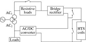
Circuit topology of SMES-SFCL


7 Prospective SMES Applications Toward Smart Grids
7.1 Application Solutions of SMES in the Modern Power Systems
To cope with modern power systems, large-scale, medium-scale, and small-scale SMES devices with different energy storage capacity and power rating are demanded. In this section, four SMES units as shown in Table 6 are introduced to discuss and verify the application schemes and characteristics of SMES for power generation, transmission, distribution, and end-users.
7.1.1 Analysis on Daily Load Levelling
Daily load leveling refers to the use of electric energy stored in the large-scale ESSs during the time periods of low demand to supply peak demand. Large-scale pumped hydro storage (PHS) technology with a typical storage efficiency between 70 and 80 % is currently the commercial storage option for daily load leveling. It has been reported [66] that a TJ-class SMES device with high storage efficiency of ~90 % and no site limitation will be a promising solution in the future. Although the capital cost of an SMES device is more than that of a PHS device with the same capacity at present, SMES will reduce the annual operation cost for the same capital cost to 50–60 % of that of PHS, thus the overall life cycle cost of SMES may be lower than that of PHS.
Figure 38 shows a typical curve of a 3.6 TJ SMES device for daily load leveling: (i) During the low demand time periods, the 3.6 TJ SMES device in Scheme 1 is operated at energy charge state to absorb the surplus power P min − P demand, and thus the base-load power plants can be operated efficiently at full power P min; (ii) During the peak demand time periods, the 3.6 TJ SMES device will be operated at energy discharge state to release the stored energy to compensate the shortfall power P demand − P max for satisfying the real-time load power demand P demand, which reduces the need to draw an electricity from the peaking power plants or increase the grid infrastructures; (iii) During the medium-demand time periods, the practical electricity generated P generated can basically follow with the P demand, and the 3.6 TJ SMES device is operated at energy storage state with nearly zero energy loss.

The results of 3.6 TJ SMES for daily load leveling. a The power changes of daily demand and supply with SMES; b The energy changes of the 3.6 TJ SMES device
The energy practically stored in the 3.6 TJ SMES device fluctuates along with the dynamic energy exchange processes, and can be calculated by
where E 0, initial stored energy; P r (t), the surplus or shortfall power. In the case of sinusoidal AC power and energy exchange, P r (t) approximately equals to the root mean square (RMS) power P RMS due to the equivalence of the AC to DC power conversion, thus the absorbed or released energy equals to the product of P RMS and time duration Δt.
Since the 3.6 TJ SMES device can be controlled to fully compensate the reference power demand when I SMES(t) is greater than or equal to the RMS current I RMS, the maximum compensation time duration can be calculated by
where I max is the maximum allowable operation current through the HTS coil, which should be limited within its critical current to avoid the occurrence of quench.
Figure 39 shows the results of T comp versus I max with L SMES = 72 kH and E SMES = 3.6 TJ. For a specific coil inductance, T comp is almost proportional to the square of I max. For a specific energy storage capacity, T comp increases rapidly with increment of I max at first and then approaches a saturation value gradually. A reasonable parameter optimization should be achieved by considering the external power demands and development specifications of the HTS coil, e.g., the capital cost [67] for developing a large-scale HTS coil with large coil inductance, the refrigeration cost [68] for achieving a ultra-low operation temperature with high critical current. What is more, the coil structure should also be optimized to reduce the electromagnetic force and stray magnetic field for further improving the critical current and lessening the electromagnetic pollutions. The multipole solenoidal coil [33] and toroidal coil [14] are normally applied at present. Recently, three new kinds of force-balanced coil (FBC) [69], stress balanced coil (SBC) [70], and tilted toroidal coil (TTC) [71] have been introduced for large-scale coil developments.

T comp versus I max with L SMES = 72 kH and E SMES = 3.6 TJ
7.1.2 Analysis on Load Fluctuation Compensation
As mentioned above, a TJ-class SMES or PHS device is available for daily load leveling. However, there are still some second-level or minute-level load fluctuations during the medium-demand time periods. A GJ class SMES device seems to be a more economical option for these load fluctuation compensation applications in the power transmission systems. Currently, two ongoing 2.4 GJ YBCO SMES [14] and 48 GJ MgB2 SMES [42] projects are proposed to carry out the load fluctuation compensations from hundreds of MW to GW class.
Figure 40 shows the results of SMES for minute-level load fluctuation compensations. Since SMES has the shortest response time to absorb or release the electricity as compared to other ESSs, the introduction of the 36 GJ SMES device in Scheme 2 makes the dynamic compensation more effective and timely.

The results of 36 GJ SMES for load fluctuation compensation. a The power changes of demand fluctuation and supply with SMES; b The energy changes of the 36 GJ SMES device
The relations between the capital cost and energy storage capacity in an SMES device are shown in Fig. 41, and the capital cost equations [67] for a solenoidal coil and toroidal coil can be approximatively expressed by Cost (M$) = 0.95 [Energy (MJ)]0.67 and Cost (M$) = 2.04 [Energy (MJ)]0.5.

Cost (M$) versus Energy (MJ) for solenoidal and toroidal coils
The capital costs of the 3.6 TJ and 36 GJ SMES coils are 3870.6 and 387.1 M$, respectively. To reduce the capital cost and make better use of an SMES device, the SMES can be introduced to combine with other ESSs for forming a hybrid energy storage system (HESS). The HESS has very high reliability because the hybrid combinations of several ESSs can combine to use their advantages in full, but compensate for each other’s disadvantages. A typical case is the LIQHYSMES storage unit (LSU) [42] consisting of 125 GWh LH2 and 48 GJ SMES, which has the advantages of fast response speed, high power density, and high energy density. Therefore, the 36 GJ SMES device can be used not only for short-time load fluctuation compensations, but also for daily load leveling by combining with a large-scale PHS device. The above HESS concept provides an economical way for smart power generation and transmission management.
7.1.3 Analysis on Voltage Fluctuation Compensation
Since the power density of SMES is about 100 times higher than that of a redox flow battery, and about 10 times higher than those of a lead-acid battery and NaS battery [72], SMES can provide much larger exchanging power as compared to the battery energy storage (BES) for the same mass and volume. Moreover, the grid voltage fluctuations can be compensated within a quarter of power-frequency cycle because the response time of SMES is generally about 1–5 ms, however, the first cycle compensation cannot be practically achieved with BES. Therefore, a number of MJ-class and MW-level SMES devices [34–41] have been developed in the world for the studies of the potential replacement of BES in the power distribution systems.
According to (12), T comp equals to several seconds for the MW-level fluctuation compensations if the 3.6 MJ SMES device in Scheme 3 is applied. To further enlarge T comp, a larger energy storage capacity is needed. For instance, the 36 GJ SMES device in Scheme 2 can bring a very large T comp of about 9 h, however, the high capital cost makes the scheme uneconomical. In view of the economy and practicability of the current SMES technology, some small-scale HESSs [13, 30, 31] have been studied and verified that the introduction of SMES with fast response speed and high power density can improve the dynamic performance of HESS, especially for solving ms-level power quality problems. Figure 42 shows the results of a typical SMES-BES HESS for voltage fluctuation compensations. The 36 kJ SMES device in Scheme 4 is only applied to absorb or release 20 kJ electric energy to compensate the 1 MW voltage swell or sag within the first 20 ms, and then the BES will continue to carry out the voltage fluctuation compensations for a much longer time.

The results of HESS for voltage fluctuation compensation. a The voltage changes of the load with HESS; b The energy changes of the 36 kJ SMES device
7.2 Application Prospects and Considerations of SMES in Future Smart Grid
The alternatives for the continued availability of a highly reliable and inexpensive power supply in future SGs include the deployment of clean coal generation, nuclear power generation, renewable energy generation, and other generation resources. Various ESSs can be used to allow increased capacity and stability to be derived from any given quantity of physical resources, and should be considered as a strategic choice that allows for optimum use of existing and new resources of all kinds. The overview and application analyses of the current SMES technology conclude that SMES has the significant potential to combine with, and even replace other ESSs in modern power systems. It is expected that the future SMES devices are not only essential to improve the power quality with small-scale or medium-scale energy storage capacity but also ensure the daily load leveling and overall reliability of the power systems with large-scale energy storage capacity.
7.2.1 Application Prospects of SMES in Future Smart Grids
Figure 43 shows the application prospects of SMES for future SGs [73]. The main SMES application schemes and their basic functions are described as follows: (i) SMES installed near the large-scale centralized generators (CGs) is used to balance the output power and to achieve daily load leveling; (ii) SMES installed in the transmission lines (TLs) is used to form FACTS devices for compensating the load fluctuations and maintaining the grid frequency stability; (iii) SMES installed in the distribution lines (DLs) is used to form DFACTS devices for improving the power quality; (iv) SMES installed near the DGs is used to reduce the impacts from the intermittent RESs and to facilitate the grid integration; (v) SMES installed near the power end-users is used to form SMES-based UPSs for enhancing the stability of electricity and protecting the critical loads.

The application prospects of SMES in future SGs
The requirements of a single SMES unit in the above five application schemes are shown in Table 7. Besides the application solution of sole SMES with full energy storage scale, three additional application solutions of SMES should be considered in future SGs.
The first solution is to install a number of SMES devices with very high power rating and very low energy storage capacity near the commercial ESS devices for forming an SMES-based HESS. As compared to the application solution of sole SMES, SMES in a HESS is only used to compensate the initial fluctuations of electricity for a very short-time period. For instance, the 10 GJ class SMES can be used to carry out the daily load leveling for a few minutes before the initial operation of large-scale PHS, and to compensate some rapid load fluctuations during the whole day. The 10 kJ class SMES can be used to improve the power quality and stability for one or a few power-frequency cycles before the initial operation of medium-scale BES.
The HESS technology will greatly reduce the capital cost of ESSs in different power system applications. Figure 44 shows the results of K cost versus K energy with solenoidal coil and toroidal coil. K energy is the ratio between the SMES energy storage capacity needed in a HESS and the energy storage capacity in a sole SMES. K cost is the ratio between the SMES capital cost needed in a HESS and the capital cost in a sole SMES. It is noticed that K cost ≈ 0.1 when K energy = 0.01 for large-scale toroidal coil developments, and K cost ≈ 0.45 when K energy = 0.01 for medium-scale and small-scale solenoidal coil developments.

K cost versus K energy with solenoidal coil and toroidal coil
The second solution is to distribute several small-scale SMES units in different locations and to make all the SMES units work harmoniously by combined control of each SMES. This so-called distributed SMES (DSMES) technology has already been commercially deployed and operated [74]. The DSMES technology has the advantages of high mobility and high expandability because the SMES units in the trucks are easy to install in arbitrary locations once they arrives on site. The results reported [43] indicate that the DSMES technology behaves better in performance than the concentrated installation of a large-scale SMES unit.
The third solution is to combine the HESS and DSMES technologies and to distribute a number of HESS units in large, medium, and small scales for the power generation, transmission, distribution, and end-users. The distributed HESS (DHESS) technology having the advantages of both HESS and DSMES will provide very efficient stability and reliability of the whole power system.
The comparisons of different SMES application solutions are shown in Table 8. The three improved solutions utilize various ESS devices and technologies efficiently and enhance the flexibility and economy of SMES greatly. Therefore, it can be expected that SMES will be a flexible and efficient ESS option for smart power and energy managements in future SGs.
7.2.2 Conceptual Design of a Superconducting DC Distribution Network with Superconducting DC Cable and SMES Technologies
The resistive energy losses consumed on power transmission lines become enormous as the high-capacity of power demand is required by the dramatically expanding and developed society. HTS technology is an alternative way to resolve the conventional difficulties to achieve high efficiency in power transmissions [7, 8]. The superconducting DC cable with nearly zero energy loss is favorable for low-voltage and long-distance power transmission for future power end-users. Various SMES devices with different application schemes have the potential to further enhance the stability and reliability of the superconducting DC transmissions. Figure 45 shows the conceptual design of a superconducting DC distribution network with superconducting DC cable and SMES technologies. The superconducting DC distribution network is to implement the hybrid energy transfer of the hydrogen and electricity, which has been technically verified [75–77]. The LH2 transferred can not only be used to provide hydrogen energy for the fuel cells (FCs) and FC vehicles (FCVs) [17], but also be used as the refrigeration fluid for cooling the superconducting DC cable and SMES devices, which can be developed by either HTS YBCO wires or MgB2 wires.

Conceptual design of a superconducting DC distribution network
The application schemes of SMES in the superconducting DC distribution network are described as follows: (i) SMES and HESS devices installed in the cable terminal and middle parts are used to enhance the power transmission capacity and to maintain the voltage stabilization; (ii) DSMES and DHESS trucks with highly mobile and expandable characteristics are used to further improve the integrated performance of scheme (i) in arbitrary locations or time periods; (iii) SMES devices installed in the DC bus of local PV cells or FCs are used to maintain the output voltage stabilization for connecting with the DC distribution network and improving the reliability of electricity in off-grid loads; (iv) SMES devices installed near the on-grid loads are used to serve as fast response and high power UPSs; (v) SMES devices installed in FCVs are used to enhance the fast repeated charge–discharge performance and further to enhance the reliability of the vehicle-to-grid (V2G) [78] and vehicle-to-building (V2B) technologies [79].
The superconducting DC distribution network is able to operate with very high current density and very low voltage allowing direct connection of the generators to the local power end-users, eliminating the need for high voltage insulation and transformers. For the same power delivery as in the typical 110–1000 kV conventional transmission system, if a superconducting DC cable with the operation current ranging from thousands of amperes to tens of thousands of amperes is applied, the operation voltage might be greatly reduced to thousands of volts.
Figure 46 shows an analytical case of the superconducting DC distribution network. A 110 V rectified DC power source is applied to a 0.1 Ω load resistor through the superconducting DC cable. The energy lossy resistor from the relevant power electronic devices is assumed as 0.01 Ω. If an additional 0.5 Ω load resistor is connected in parallel from the time zero, the operation voltage across the two load resistors will decrease rapidly to about 83 V at first and then increase gradually to about 97 V, as shown in Fig. 47.

An analytical case of the superconducting DC distribution network

The results of sole SMES, DSMES, and DHESS application solutions for a DC voltage sag compensation
To maintain the practical operation voltage around their reference value of 100 V, three SMES application solutions are adopted. The first one is to install a 2 H/300 A sole SMES unit near the DC power source. The sole SMES unit can be used to compensate the dynamic load fluctuations in different superconducting DC cables, however, the inductive and capacitive reactance from the long-distance cable limits the practical response speeds. As shown in Fig. 47, there is still an inevitable voltage drop from 0 to about 0.24 s.
The second one is to distribute several DSMES units in different cables or in different locations along a specific cable. The DSMES unit located at the terminal of a superconducting DC cable in Fig. 46 can be directly applied to compensate the voltage sag within several milliseconds, which results in an effective and timely voltage sag compensation process.
The third one is to combine the small-scale DSMES units with several local ESSs, e.g., BES, to form a DHESS. The DSMES unit is only applied to compensate the voltage sag within the first 20 ms, which reduces the energy storage capacity and capital cost of the DSMES units.
References
Jin JX, Zhang CM, Guo YG, Zhu JG (2007) Theory and operation principle of a HTS high Q resonant circuit. IEEE Trans Appl Supercond 17(2):2022–2025
Jin JX (2007) HTS energy storage techniques for use in distributed generation systems. Phys C 460–462:1449–1450
Jin JX (2007) High efficient DC power transmission using high-temperature superconductors. Phys C 460–462:1443–1444
Jin JX, Zheng LH, Guo YG, Zhu JG, Grantham C, Sorrell CC, Xu W (2012) High-temperature superconducting linear synchronous motors integrated with HTS magnetic levitation components. IEEE Trans Appl Supercond 22(5):5202617 (17 pages)
Jin JX, Zheng LH, Guo YG, Zhu JG (2011) Performance characteristics of an HTS linear synchronous motor with HTS bulk magnet secondary. IEEE Trans Ind Appl 47(6):2469–2477
Zheng LH, Jin JX, Guo YG, Xu W, Zhu JG (2012) Performance analysis of a double-sided HTSLSM for a HTS magnetic suspension system. IEEE Trans Magn 48(2):655–658
Jin JX, Zheng LH, Xu W, Guo YG, Zhu JG (2011) Influence of external traveling-wave magnetic field on trapped field of a high temperature superconducting bulk magnet in a linear synchronous motor. J Appl Phys 109(11):113913-1–113913-4
Jin JX, Zheng LH, Guo YG, Xu W, Zhu JG (2011) Analysis and experimental validation of an HTS linear synchronous propulsion prototype with HTS magnetic suspension. Phys C 471(1–2):520–527
Jin JX, Grantham C, Dou SX, Liu HK, Zeng ZJ, Liu ZY, Blackburn TR, Li XY, Liu HL, Liu JY (1997) Electrical application of high T c superconducting saturable magnetic core fault current limiter. IEEE Trans Appl Supercond 7(2):1009–1012
Jin JX, Dou SX, Liu HK, Grantham C (1997) High voltage generation with a high T c superconducting resonant circuit. IEEE Trans Appl Supercond 7(2):881–884
Jin JX, Dou SX, Grantham C, Liu HK (1995) Preparation of high T c superconducting coils for consideration of their use in a prototype fault current limiter. IEEE Trans Appl Supercond 5(2):1051–1054
Chakraborty A (2011) Advancements in power electronics and drives in interface with growing renewable energy resources. Renew Sustain Energy Rev 15:1816–1827
Jin JX (2011) High temperature superconducting energy storage technologies: principle and application. Science Press, Beijing
Shikimachi K, Hirano N, Nagaya S, Kawashima H, Higashikawa K, Nakamura T (2009) System coordination of 2 GJ class YBCO SMES for power system control. IEEE Trans Appl Supercond 19(3):2012–2018
Pahlevaninezhad M, Drobnik J, Jain PK, Bakhshai A (2012) A load adaptive control approach for a zero-voltage-switching DC/DC converter used for electric vehicles. IEEE Trans Industr Electron 59(2):920–933
Kim HS, Ryu MH, Baek JW, Jung JH (2013) High-efficiency isolated bidirectional AC–DC converter for a DC distribution system. IEEE Trans Power Electron 28(4):1642–1654
Morandi A, Trevisani L, Negrini F, Ribani PL, Fabbri M (2012) Feasibility of superconducting magnetic energy storage on board of ground vehicles with present state-of-the-art superconductors. IEEE Trans Appl Supercond 22(2):5700106
Hamajima T, Amata H, Iwasaki T, Atomura N, Tsuda M, Miyagi D, Shintomi T, Makida Y, Takao T, Munakata K, Kajiwara M (2012) Application of SMES and fuel cell system combined with liquid hydrogen vehicle station to renewable energy control. IEEE Trans Appl Supercond 22(3):5701704
Kakigano H, Miura Y, Ise T (2012) Low-voltage bipolar-type DC microgrid for super high quality distribution. IEEE Trans Power Electron 25(12):3066–3075
Salomonsson D, Sannino A (2007) Low-voltage DC distribution system for commercial power systems with sensitive electronic loads. IEEE Trans Power Deliv 22(3):1620–1627
Furuse M, Fuchino S, Higuchi N, Ishii I (2005) Feasibility study of low-voltage DC superconducting distribution system. IEEE Trans Appl Supercond 15(2):1759–1762
Nakayama T, Yagai T, Tsuda M, Hamajima T (2009) Micro power grid system with SMES and superconducting cable modules cooled by liquid hydrogen. IEEE Trans Appl Supercond 19(3):2062–2065
Jin JX, Chen XY, Zhou X, Xu W, Zhang YC, Xin Y (2013) Development of a new bridge-type chopper for low-voltage SMES applications. In: 2013 IEEE energy conversion congress and exposition (ECCE), Denver, Colorado, USA, September 15, 2013, pp 5258–5265
Bibian S, Jin H (2000) Time delay compensation of digital control for DC switch mode power supplies using prediction techniques. IEEE Trans Power Electron 15(5):835–842
Bae BH, Sul SK (2003) A compensation method for time delay of full-digital synchronous frame current regulator of PWM AC drives. IEEE Trans Ind Appl 39(3):802–810
Tomita M, Murakami M, Nariki S, Sawa K (2002) Mechanical persistent current switch made of resin-impregnated bulk superconductors. Supercond Sci Technol 15(5):846–849
Hayashi H, Sannomiya T, Kimura H, Tsutsumi K, Yamashita Y, Kuboyama R, Sato S, Takeo M, Ishii T, Asano K, Okada S (2001) Connecting tests of superconducting persistent-current-switch in a type of current transformer to 1 kWh SMES system. IEEE Trans Appl Supercond 11(1):1904–1907
Yuan WJ, Xian W, Ainslie M, Hong Z, Yan Y, Pei R, Jiang Y, Coombs TA (2010) Design and test of a superconducting magnetic energy Storage (SMES) coil. IEEE Trans Appl Supercond 20(3):1379–1382
Chen XY, Jin JX, Ma KM, Wen J, Xin Y, Gong WZ (2008) High temperature superconducting magnetic energy storage and its power control technology. J Electr Sci Technol China 6(2):137–142
Chen XY, Jin JX (2011) Development and evaluation of superconducting magnetic energy storage techniques for smart grid. Appl Supercond Electromagnet 2(1):31–35
Jin JX, Xu W, Chen XY, Zhou X, Zhang JY, Gong WZ, Ren AL, Xin Y (2012) Developments of SMES devices and potential applications in smart grids. In: IEEE conference on innovative smart grid technologies Asia (ISGT Asia), 21–24 May 2012, pp 1–6
Rogers JD, Schemer RI, Miller BL, Hauer JF (1983) 30-MJ superconducting magnetic energy storage system for electric utility transmission stabilization. Proc IEEE 71(9):1099–1107
Luongo CA, Baldwin T, Ribeiro P, Weber CM (2003) A 100 MJ SMES demonstration at FSU-CAPS. IEEE Trans Appl Supercond 13(2):1800–1805
Nagaya S, Hirano N, Moriguchi H, Shikimachi K, Nakabayashi H, Hanai S, Inagaki J, Ioka S, Kawashima S (2006) Field test results of the 5 MVA SMES system for bridging instantaneous voltage dips. IEEE Trans Appl Supercond 16(2):632–635
Wang QL, Dai YM, Zhao BZ, Song SS, Cao ZQ, Chen SZ, Zhang Q, Wang HS, Cheng JS, Lei YZ, Li X, Liu JH, Zhao SW, Zhang HJ, Xu GX, Yang ZM, Hu XN, Liu HY, Wang CZ, Yan LG (2010) Development of large scale superconducting magnet with very small stray magnetic field for 2 MJ SMES. IEEE Trans Appl Supercond 20(3):1352–1355
Kim HJ, Seong KC, Cho JW, Bae JH, Sim KD, Kim S, Lee EY, Ryu K, Kim SH (2006) 3 MJ/750 kVA SMES system for improving power quality. IEEE Trans Appl Supercond 16(2):574–577
Ottonello L, Canepa G, Albertelli P, Picco E, Florio A, Masciarelli G, Rossi S, Martini L, Pincella C, Mariscotti A, Torello E, Martinolli A, Mariani M (2006) The largest Italian SMES. IEEE Trans Appl Supercond 16(2):602–607
Nagaya S, Hirano N, Shikimachi K, Hanai S, Inagaki J, Maruyama K, Ioka S, Ono M, Ohsemochi K, Kurusu T (2004) Development of MJ-class HTS SMES for bridging instantaneous voltage dips. IEEE Trans Appl Supercond 14(2):770–773
Dai ST, Xiao LY, Wang ZK, Zhang JY, Zhang D, Hui D, Song NH, Zhang FY, Gao ZY, Wang YS, Lin LZ (2007) Design of a 1 MJ/0.5 MVA HTS magnet for SMES. IEEE Trans Appl Supercond 17(2):1977–1980
Tixador P, Bellin B, Deleglise M, Vallier JC, Bruzek CE, Pavard S, Saugrain JM (2005) Design of a 800 kJ HTS SMES. IEEE Trans Appl Supercond 15(2):1907–1910
Kim WS, Kwak SY, Lee JK, Choi KD, Jung HK, Seong KC, Hahn SY (2006) Design of HTS magnets for a 600 kJ SMES. IEEE Trans Appl Supercond 16(2):620–623
Sander M, Gehring R, Neumann H (2013) LIQHYSMES—a 48 GJ toroidal MgB2-SMES for buffering minute and second fluctuations. IEEE Trans Appl Supercond 23(3):5700505
Howe JB (2001) Distributed SMES: a new technology supporting active grid management. Mod Power Syst 21(1):27–28
Mito T, Chikaraishi H, Kawagoe A, Maekawa R, Abe R, Baba T, Okumura K, Kuge A, Iwakuma M, Sumiyoshi F (2009) Summary of a 1 MJ conduction-cooled LTS pulse coil developed for 1 MW, 1 s UPS-SMES. IEEE Trans Appl Supercond 19(3):1999–2003
Katagiri T, Nakabayashi H, Nijo Y, Tamada T, Noda T, Hirano N, Nagata T, Nagaya S, Yamane M, Ishii Y, Nitta T (2009) Field test result of 10MVA/20 MJ SMES for load fluctuation compensation. IEEE Trans Appl Supercond 19(3):1993–1998
Hayashi H, Hatabe Y, Nagafuchi T, Taguchi A, Terazono K, Ishii T, Taniguchi S (2006) Test results of power system control by experimental SMES. IEEE Trans Appl Supercond 16(2):598–601
Nomura S, Kasuya K, Tanaka N, Tsuboi K, Tsutsui H, Tsuji-Iio S, Shimada R (2008) Experimental results of a 7-T force-balanced helical coil for large-scale SMES. IEEE Trans Appl Supercond 18(2):701–704
Zhu XG, Jiang XH (2007) 150kVA/0.3 MJ current source type dynamic voltage compensation device. Power Electron Technol 41(1):1–3
Morandi A, Breschi M, Fabbri M, Negrini F, Penco R, Perrella M, Ribani PL, Tassisto M, Trevisani L (2008) Design, manufacturing and preliminary tests of a conduction cooled 200 kJ Nb–Ti μSMES. IEEE Trans Appl Supercond 18(2):697–700
Koyanagi K, Ohsemochi K, Takahashi M, Kurusu T, Tosaka T, Ono M, Ishii Y, Shimada K, Nomura S, Kidoguchi K, Onoda H, Hirano N, Nagaya S (2006) Design of a high energy-density SMES coil with Bi-2212 cables. IEEE Trans Appl Supercond 16(2):586–589
Wang QL, Dai YM, Song SS, Wen HM, Bai Y, Yan LG, Kim K (2008) A 30 kJ Bi2223 high temperature superconducting magnet for SMES with solid-nitrogen protection. IEEE Trans Appl Supercond 18(2):754–757
Shi J, Tang YJ, Zhou YS, Chen JL, Xu DH, Wang HL, Lu YF, Ren L, Wei B, Li JD, Cheng SJ (2007) Development of a conduction-cooled HTS SMES. IEEE Trans Appl Supercond 17(3):3846–3852
Kwak SY, Lee S, Lee S, Kim WS, Lee JK, Park C, Bae J, Song JB, Lee H, Choi K, Seong K, Jung H, Hahn SY (2009) Design of HTS magnets for a 2.5 MJ SMES. IEEE Trans Appl Supercond 19(3):1985–1988
Kreutz R, Salbert H, Krischel D, Hobl A, Radermacher C, Blacha N, Behrens P, Dütsch K (2003) Design of a 150 kJ high-Tc SMES (HSMES) for a 20 kVA uninterruptible power supply system. IEEE Trans Appl Supercond 13(2):1860–1862
Kozak J, Kozak S, Janowski T, Majka M (2009) Design and performance results of first polish SMES. IEEE Trans Appl Supercond 19(3):1981–1984
Hawley CJ, Gower SA (2005) Design and preliminary results of a prototype HTS SMES device. IEEE Trans Appl Supercond 15(2):1899–1902
Ali MH, Wu B, Dougal RA (2010) An overview of SMES applications in power and energy systems. IEEE Trans Sustain Energ 1(1):38–47
Liu CJ, Hu CS, Li X, Chen M, Xu DF (2008) Design of SMES control system for smoothing power fluctuations in wind farms. Autom Electr Power Syst 32(16):84–88
Tam KS, Kumar P, Foreman M (1989) Enhancing the utilization of photovoltaic power generation by superconductive magnetic energy storage. IEEE Trans Energy Convers 4(3):314–321
Jung HY, Kim AR, Kim JH, Park M, Yu IK, Kim SH, Sim K, Kim HJ, Seong KC, Asao T, Tamura J (2009) A study on the operating characteristics of SMES for the dispersed power generation system. IEEE Trans Appl Supercond 19(3):2028–2031
Padimiti DS, Chowdhury BH (2007) Superconducting magnetic energy storage system (SMES) for improved dynamic system performance. In: Power engineering society general meeting, 24–28 June 2007, pp 1–6
Zheng L, Ma WA (2000) Application of SMES system with a comprehensive control for enhancing transient stability. In: International conference on advances in power system control, operation and management, Oct. 30–Nov. 1, 2000, pp 225–229
Ali MH, Murata T, Tamura J (2005) A fuzzy logic-controlled superconducting magnetic energy storage (SMES) unit for augmentation of transient stability. In: International conference on power electronics and drives systems, 2005, vol 2, pp 1566–1571
Kim AR, Kim GH, Kim JH, Ali MH, Park M, Yu IK, Kim HJ, Kim SH, Seong KC (2008) Operational characteristic of the high quality power conditioner with SMES. IEEE Trans Appl Supercond 18(2):705–708
Zhu GP, Wang ZJ, Zhang GQ (2005) Research on a combined device SMES-SFCL based on multi-object optimization. IEEE Trans Appl Supercond 15(2):2019–2022
Nomura S, Shintomi T, Akita S, Nitta T, Shimada R, Meguro S (2010) Technical and cost evaluation on SMES for electric power compensation. IEEE Trans Appl Supercond 20(2):101–106
Green MA, Strauss BP (2008) The cost of superconducting magnets as a function of stored energy and design magnetic induction times the field volume. IEEE Trans Appl Supercond 18(2):248–251
Van Sciver SW (2001) Cryogenic systems for superconducting devices. Phys C 354(1–4):129–135
Nomura S, Chikaraishi H, Tsutsui H, Shimada R (2013) Feasibility study on large scale SMES for daily load leveling using force-balanced helical coils. IEEE Trans Appl Supercond 23(3):5700904
Nomura S, Yamagnta K, Watauabe N, Ajiki D, Ajikawa H, Koizumi E, Shimada R (2000) Experiment of HTS stress-balanced helical coil. IEEE Trans Appl Supercond 10(1):792–795
Fabbri M, Ajiki D, Negrini F, Shimada R, Tsutsui H, Venturi F (2003) Tilted toroidal coils for superconducting magnetic energy storage systems. IEEE Trans Magn 39(6):3546–3550
Kondoh J, Ishii I, Yamaguchi H, Murata A, Otani K, Sakuta K, Higuchi N, Sekine S, Kamimoto M (2000) Electrical energy storage systems for energy networks. Energy Convers Manag 41(17):1863–1874
Jin JX, Chen XY (2012) Study on the SMES application solutions for smart grid. Physics Procedia 36:902–907
Lee SJ (2007) Location of a superconducting device in a power grid for system loss minimization using loss sensitivity. IEEE Trans Appl Supercond 17(2):2531–2534
Bossel U (2006) Does a hydrogen economy make sense? Proc IEEE 94(10):1826–1837
Yamada S, Hishinuma Y, Uede T, Schippl K, Yanagi N, Mito T, Sato M (2010) Conceptual design of 1 GW class hybrid energy transfer line of hydrogen and electricity. J Phys Conf Ser 234:032064
Shintomi T, Makida Y, Hamajima T, Tsuda S, Miyagi D, Takao T, Tanoue N, Ota N, Munakata K, Miwa Y (2012) Design study of SMES system cooled by thermo-siphon with liquid hydrogen for effective use of renewable energy. IEEE Trans Appl Supercond 22(3):5701604
Liu H, Ning HS, Zhang Y, Guizani M (2013) Battery status-aware authentication scheme for V2G networks in smart grid. IEEE Trans Smart Grid 4(1):99–110
Pang C, Dutta P, Kezunovic M (2012) BEVs/PHEVs as dispersed energy storage for V2B uses in the smart grid. IEEE Trans Smart Grid 3(1):473–482
Acknowledgments
The author thanks X. Y. Chen who assisted this work, and also the support from Y. Xin, Y. G. Guo, J. G. Zhu, and C. Grantham.
Author information
Authors and Affiliations
Corresponding author
Editor information
Editors and Affiliations
Rights and permissions
Copyright information
© 2014 Springer Science+Business Media Singapore
About this chapter
Cite this chapter
Jin, J.X. (2014). Emerging SMES Technology into Energy Storage Systems and Smart Grid Applications. In: Hossain, J., Mahmud, A. (eds) Large Scale Renewable Power Generation. Green Energy and Technology. Springer, Singapore. https://doi.org/10.1007/978-981-4585-30-9_4
Download citation
DOI: https://doi.org/10.1007/978-981-4585-30-9_4
Published:
Publisher Name: Springer, Singapore
Print ISBN: 978-981-4585-29-3
Online ISBN: 978-981-4585-30-9
eBook Packages: EnergyEnergy (R0)