
Abstract
Acquiring high-content images of 3D-cultured cells for analyzing multiple cellular events is a daunting task, requiring an automated fluorescent microscope and high-throughput image analysis software. High throughput is an important feature for high-content imaging (HCI) devices to enable rapid image acquisition. Various factors come into play when dealing with the speed of image acquisition. For example, capturing large number of cells with lower magnification or reducing sample volume/size can increase data acquisition speed. In addition, reducing exposure time with the use of high intensity light sources, optimizing fluorescence staining protocols for brighter colors, and using an objective lens with relatively high numerical aperture also significantly increases the image acquisition speed [1].
Access provided by Autonomous University of Puebla. Download chapter PDF
Keywords
These keywords were added by machine and not by the authors. This process is experimental and the keywords may be updated as the learning algorithm improves.
6.1 Introduction
Acquiring high-content images of 3D-cultured cells for analyzing multiple cellular events is a daunting task, requiring an automated fluorescent microscope and high-throughput image analysis software. High throughput is an important feature for high-content imaging (HCI) devices to enable rapid image acquisition. Various factors come into play when dealing with the speed of image acquisition. For example, capturing large number of cells with lower magnification or reducing sample volume/size can increase data acquisition speed. In addition, reducing exposure time with the use of high intensity light sources, optimizing fluorescence staining protocols for brighter colors, and using an objective lens with relatively high numerical aperture also significantly increases the image acquisition speed [1].
The basic components of any imaging device consist of light sources, detectors, objective lenses, and optical filters among which light sources and detectors play critical role in determining fate of any HCI system. Light sources can comprise of lamps, lasers, and light-emitting diodes (LEDs) with each of them having their own benefits and limitations. For example, lamps provide a broad excitation source from UV to IR, but should be replaced frequently due to shorter lifetime and may need realignment for optimal excitation. Lasers, on the other hand, have longer lifetime, but may not offer optimal excitation spectra for certain target fluorophores such as blue fluorescent dyes. LEDs offer both long lifetime and optimal excitation, but are expensive. Most of currently available image acquisition systems use xenon or mercury lamps as a light source due to economic feasibility and a broad range of spectra. Detectors are another important component of HCI devices with two types of detectors commonly used. These detectors are charge-coupled devices (CCDs) and photomultiplier tubes (PMTs). CCD-based detectors are widely used in HCI devices as it offers excellent acquisition speed (100 frames per second), large dynamic ranges (>20,000:1), broad spectral sensitivity (400–900 nm and higher), and high resolution (>2000 × 2000 pixels), but with reduced sensitivity to low intensity light. On the other hand, PMT-based detectors offer high sensitivity towards low intensity light, but with compromise in throughput. Multiple PMTs are used in parallel to acquire images through various fluorescent channels [1–3].
Conventional HCI devices can be divided broadly into two categories; wide-field imaging devices and confocal imaging devices. Wide-field imaging devices are basically inverted microscopes which offer an excellent image acquisition speed. Some examples of commercially available CCD-based wide-field imaging devices are ArrayScan XTI HCS Reader manufactured by Thermo Fisher, IN Cell Analyzer 2000 by GE Healthcare, ImageXpress Micro HCS system by Molecular Devices, Operetta by Perkin Elmer, WiSCAN by IDEA Bio-Medical, and S+ Scanner by SEMCO. These commercially available wide-field imaging devices commonly use lamps and LEDs as their light source. For example, ArrayScan XTI HCS Reader uses a metal halide lamp and LED, and IN Cell Analyzer 2000 uses a metal halide lamp. Similarly, ImageXpress Micro HCS system uses a xenon lamp, and Operetta uses a xenon lamp and LED. In addition, S+ scanner uses a mercury lamp, and WiSCAN uses a mercury lamp and LED. Although different types of light sources are used by various wide-field imaging devices, the difference is very little in terms of optical performance. The difference between the various wide-field imagers available arise generally from the numerical aperture of the objectives and the quality of light path [1, 4, 5].
Confocal imaging devices use light barrier with a fixed or adjustable pinhole to eliminate light in front or behind the focus plane of an objective. Confocal devices offer high resolution and improved contrast compared to wide-field devices, but it also causes reduction in light signal and only scans single points of a specimen at any given moment. Although these issues have been overcome by using technologies like laser scanning confocal microscopy (LSCM) and Nipkow spinning disk, the image acquisition speed is compromised, and there is always a chance of photobleaching [1, 4, 6, 7]. Confocal imaging devices are expensive compared to wide-field imaging devices and most of its applications are towards imaging small intracellular structures, small cells, complex 3D structures, etc. IN Cell Analyzer 6000 by GE Healthcare is a commonly used confocal microscope, which uses LSCM with varying apertures. It consists of four laser lines and a LED for transmitted light and a scientific complementary metal oxide semiconductor (sCMOS)-based detector. ImageXpress ULTRA developed by Molecular devices is another confocal imager consisting of four lasers and four PMTs that can be operated serially or in parallel [1, 8, 9]. Extensive information on various HCI devices and their components can be found in Assay Guidance Manual published by Eli Lilly & Company and the National Center for Advancing Translational Sciences (http://www.ncbi.nlm.nih.gov/books/NBK53196/) [1].
While other HCI devices are highly sophisticated and require trained personnel to operate the machine, the S+ Scanner offers researchers/users the ability to acquire high quality fluorescent images in a high-throughput manner without the need of complex training. This chapter aims to provide simple procedures for operating S+ Scanner to rapidly acquire 3D-cultured cell images from the micropillar/microwell chip platform.
6.2 Materials
-
Micropillar/microwell chips (25 × 75 × 2 mm from Samsung Electro-Mechanics, Co. or SEMCO, Suwon, South Korea)
-
S+ MicroArrayer with six solenoid valves and ceramic tips (SEMCO, Suwon, South Korea)
-
S+ Scanner with four filter sets (SEMCO, Suwon, South Korea)
-
Light source (Olympus, Model: U-HGLGPS)
-
Micropillar chip zig (SEMCO, Suwon, South Korea)
-
Microwell chip zig part I and II (SEMCO, Suwon, South Korea)
-
Metal frame for the micropillar chip (SEMCO, Suwon, South Korea)
6.3 Protocols
S+ Scanner, is a wide-field imager consisting of a mercury lamp as a light source and a CCD-based detector. It is an automated fluorescence microscope with four filter channels for detecting multicolor, blue, green, and red fluorescent dyes, individually or simultaneously. The basic components of S+ Scanner are provided in Fig. 6.1. Certain precautions are required before starting the image acquisition from the micropillar/microwell chips. For example, micropillar chips stained with fluorescent dyes should be dried properly before scanning to avoid damage to the objective lens and stored in the dark to prevent photobleaching. In addition, when acquiring the image from microwell chips containing liquid samples it should be covered with a gas-permeable sealing membrane to prevent spilling of the samples and to minimize immediate drying of the spots.

Mechanical components of S+ Scanner
6.3.1 Daily Operational Procedures
-
1.
Turn on the power source (by using the blue switch on the step-up transformer).
-
2.
Turn on the S+ Scanner using the green power switch and then press the ‘Reset’ button (Fig. 6.2). Note: Pushing the ‘Reset’ button resets XYZ coordinates of the chip-loading deck. This step is essential to avoid malfunctioning of the S+ Scanner. Do not skip this step!
Fig. 6.2 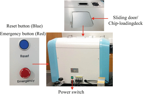
The picture of S+ Scanner showing the power switch on the back, reset and emergency buttons on the side, and sliding door/chip-loading deck on the top

-
3.
Turn on the light source and the computer. Use the black switch on the back to turn on the light source and the ‘ON/OFF’ button in the front to turn on the lamp (Fig. 6.3). Note: After the lamp is turned ON, do not turn OFF for 2 min to avoid damage to the lamp. In addition, do not turn ON the lamp within 10 min of turning OFF. The operation of switches is disabled for 5 min after the lamp is turned OFF. The lamp is connected to the light source in S+ Scanner via a fiber optic cable, which needs to be placed properly to avoid damage to the fiber optic cable.
Fig. 6.3 
Pictures of the light source: (a) The front side with ON/OFF and Reset buttons and a LED indicator displaying the burner status and (b) The back side with the main switch and the fiber optic cable

-
4.
Open the scanner program by double clicking the shortcut of S+ Scanner located on the desktop (Fig. 6.4).
Fig. 6.4 
The shortcut of S+ Scanner program

-
5.
The user interface of the scanner program will be opened (Fig. 6.5).
Fig. 6.5 
The user interface of S+ Scanner program showing ‘Home’ window highlighted in a red box

-
6.
Make sure that the sliding door on top of the scanner is closed (Fig. 6.2).
-
7.
In the ‘Home’ window, click the ‘Home’ icon in the ‘XYZ Move’ tab to activate the ‘Chip loading’ and ‘Live’ icon (Fig. 6.6).
Fig. 6.6 
‘Home’ window in the user interface of the scanner program

-
8.
Click ‘Chip loading’ icon in the ‘XYZ Move’ tab to bring the chip-loading deck in position for loading the micropillar chip zig (Fig. 6.6).
-
9.
In order to place micropillar chips on the micropillar chip zig and load it into the chip-loading deck, follow the steps below (Fig. 6.7).
-
(a)
Align a metal frame on a micropillar chip by holding the metal frame at an angle of 45° against the edge of the micropillar chip (Fig. 6.7A). The dents at the bottom of the metal frame should be perfectly aligned with the circles at the bottom of the micropillar chip.
Fig. 6.7 
Preparation of micropillar chips before loading on the chip-loading deck for image acquisition. (a) Placing a metal frame on the micropillar chip at an angle of 45°, (b) Inserting all the micropillars into the holes on the metal frame, (c) Placing the micropillar chip with the metal frame on the magnetic micropillar chip zig. The circle highlighted in yellow indicates the bottom of the zig aligned with the bottom of the micropillar chip.
-
(b)
Slowly drop the metal frame so that all the micropillars go into the holes on the metal frame (Fig. 6.7B).
-
(c)
Gently insert the micropillar chip with the metal frame into the magnetic micropillar chip zig by holding the side of the chip with two fingers (Fig. 6.7B).
-
(d)
The micropillar chip will be laid flat and held firmly while scanning due to strong magnets in the micropillar chip zig (Fig. 6.7C). Note: The strong magnetic attraction between the zig and the metal frame may impose severe force on the micropillar chip. Therefore, make sure that all the micropillars go into the holes on the metal frame properly before placing it on the zig.
-
(a)

-
10.
Open the sliding door and load the micropillar zig with the chips into the chip-loading deck by inverting the zig (Fig. 6.8). Note: The symbol (4) on the zig faces the same direction as the symbol on the chip-loading deck.
Fig. 6.8 
The micropillar chip zig with micropillar chips loaded into the chip-loading deck. The symbol (4) on the micropillar chip zig should be aligned in the same direction with the symbol (4) on the chip-loading deck.

-
11.
In case of scanning microwell chips, the chip should be sealed with a gas-permeable membrane to prevent water evaporation in the microwells and spilling of the sample over the objective lens.
-
12.
A microwell chip zig consists of two parts—part I is an open metal frame for placing microwell chips and part II is a magnetic frame that can hold the microwell chips firmly while scanning due to strong magnets (Fig. 6.9).
Fig. 6.9 
(a) A microwell chip inserted in the part I microwell chip zig, (b) The front side of the part II microwell chip zig, (c) The part I zig combined with the part II zig, and (d) The back side of the part II zig combined with the part I zig. The symbol (4) on the back of the part II zig highlighted in red should be aligned with the bottom of the microwell chips inserted.
-
13.
In order to place microwell chips on the microwell chip zig and load it into the chip-loading deck, follow the steps below (Fig. 6.9).
-
(a)
Place and insert microwell chips in the part I microwell chip zig (Fig. 6.9A) so that the back side of the microwell chip is exposed for scanning while the front side of the chip is sealed with the gas-permeable membrane, facing the part II microwell chip zig (Fig. 6.9B).
-
(b)
Take the part II zig and place it on the part I zig so that the symbol [4] on the part II zig is aligned with the bottom of the microwell chips (Fig. 6.9C, D). Note: The microwell chip will be laid flat and held firmly while scanning due to strong magnets in the microwell chip zig.
-
(a)

-
14.
Click ‘Open’ in the ‘Chip layout’ tool bar (Fig. 6.10). A window displaying a list of chip files will appear (Fig. 6.11). Note: These chip files contain XYZ coordinates for the micropillar chip and the microwell chip at different objective lenses.
Fig. 6.10 
The display of the ‘Chip layout’ tool bar
Fig. 6.11 
Window displaying a list of chip files


-
15.
Select a desired chip file from the list by clicking ‘Open’ in the ‘Chip layout’ window (Fig. 6.11). Note: Refer to parameter setting procedures to set and change XYZ coordinates in a given chip file.
-
16.
In the ‘Home’ window, click the ‘Spot position’ icon in the ‘XYZ Move’ tab to enable accurate selection of individual spots (i.e., micropillars or microwells) for live view (Fig. 6.12).
Fig. 6.12 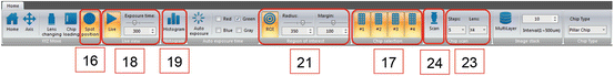
‘Home’ window of S+ Scanner program

-
17.
Select the number of chips being scanned from the ‘Chip selection’ tab in the ‘Home’ window (Fig. 6.12).
-
18.
In the ‘Live view’ tab, click the ‘Live’ icon to observe a real-time cell image and check an optimum exposure time by dragging the cursor left to right in the ‘Exposure time’ section or manually entering the value in the ‘Exposure time’ section (Fig. 6.12).
-
19.
Click the ‘Histogram’ icon in the ‘Home’ window to enable the display of fluorescence histogram (Fig. 6.12).
-
20.
To find a proper exposure time, use the ‘Histogram’ tool bar to analyze the wavelength and also visually inspect the real-time cell image. An exposure time which gives a histogram between 80 and 90 % of maximum pixel range (i.e., 255) for the given channel is considered as an optimum exposure time (Fig. 6.13). Note: Do not select too high exposure time as photobleaching of fluorescence might occur at higher exposure time.
Fig. 6.13 
‘Histogram’ window displaying the histogram of the red-fluorescent image from a red filter. The red intensity is higher than 255, meaning that the exposure time is a bit too high

-
21.
In the ‘Region of interest’ tab, click ‘ROI’ icon to display the region of interest (ROI) in the image window and use the ‘Radius’ and ‘Margin’ cursor or enter the value to increase and decrease the size of the ROI (Fig. 6.12).
-
22.
In the ‘Chip scan’ tool bar, click ‘Set’ to activate the setting window for each chip. Assign a label for each chip in the ‘Folder’ section, set the exposure time in ‘Exposure’ section, and select the desired filter from the drop-down list in the ‘Filter’ section. (Fig. 6.14). Note: A single chip can be scanned using four different filters and exposure setting depending on the user requirement. Make sure that the rest of the drop-down list in ‘Filter’ section is set to ‘UNUSED’ when scanning the chip with less than four filters setting. Select ‘Multiband’ filter for acquiring images from cells stained with multiple fluorescent dyes. The drop-down list in ‘Auto-Exp’ field is usually set to ‘UNUSED’ when scanning the chip with a user-defined exposure setting.
Fig. 6.14 
The display of the ‘Chip scan’ tool bar

-
23.
Select the magnification of an objective lens used for image acquisition from the drop down list in the ‘Lens’ field and select the number of steps for autofocus from the drop down list in the ‘Steps’ field in the ‘Chip scan’ tab (Fig. 6.12). Note: Select a larger number of steps when the chip is bent or not placed flat. It will cover a larger distance in the Z direction to obtain an optimum image in focus.
-
24.
Click the ‘Scan’ icon to begin chip scanning.
-
25.
The images obtained from individual filters are saved in multiple folders with the name of the specific filter and the exposure time used for that filter in the format of ‘filter_exposure time’ (e.g., Multiband_150). These folders are stored inside another folder with the name of the chip provided by users (Refer to Step 22). The user-named folders for multiple chips are stored in a big folder which is labeled in the format of ‘year-month-day’ (e.g., 2016-06-01).
-
26.
After the scanning is done, remove the chips from the scanner and store the scanned chips in the dark until disposed.
-
27.
Close the scanner software and turn off the computer, the S+ Scanner, and the light source (Fig. 6.3). Note: To switch off the light source, first press the ‘ON/OFF’ button in the front until the blue LED turns off and the countdown begins from 300 on the digital display. Wait until the countdown ends and then turn off the main switch of the light source located on the back.
6.3.2 Parameter Setting Procedures
6.3.2.1 Setting the Position of Filters and the Distance of Each Step for Autofocus
This tool bar displays all the list of filters available for ‘Live’ view of cells and chip scanning, allows to set and change the position of the filters, and also allows to modify the distance of each step for autofocus (Refer to Step 22). Note: The number of steps and the distance of each step are important to obtain an optimum image in focus using the autofocus function. The S+ Scanner takes multiple pictures in the Z direction but save only one best-looking image. Ideally, the distance of each step should be equal to the height of cell spheroids.
-
1.
Click ‘Move’ button to select the desired filter, which has predetermined excitation and emission spectra for image acquisition (Fig. 6.15 and Appendix). For example, clicking the ‘Move’ button for the ‘Orange’ filter enables ‘Live’ view of cells/spheroids stained with orange/red fluorescent dyes in the excitation/emission range of the ‘Orange’ filter.
Fig. 6.15 
The display of the ‘Filter’ tool bar
-
2.
Filters are set to the position displayed on the ‘Position’ column by default. Change or reset the position of individual filters only when the filter position is misplaced due to machine malfunctioning or user errors.
-
3.
To change or reset the filter position, click the ‘Set’ button to activate the ‘Filter setting’ window and enter the position of a respective filter so that ‘Live’ cell image is visible uniformly without distortion (Fig. 6.15). Note: The filter position has to be increased or decreased by few units only if needed. For example, the ‘Multiband’ filter position has to be increased or decreased to 23 or 21, respectively.
-
4.
The ‘Excitation’ and ‘Emission’ columns are used to calculate and set the distance of each step for autofocus (Fig. 6.15). Note: It doesn’t indicate actual excitation and emission wavelengths. When we select the number of ‘Steps’ in the ‘Chip scan’ tab for autofocus (Fig. 6.12), it uses the distance of each step (i.e., the thickness of one step) calculated from the following formula.

where NA is numerical aperture.
For example, when 4× and 20× lenses are used at the emission wavelength of 500 nm, the distance of each step is calculated as follows:
where the numerical apertures for the 4× lens and the 20× lens are 0.13 and 0.5, respectively.
Note: The recommended distance of each step is 10–20 μm (e.g., 400 nm emission wavelength with 4× lens) for 3D-cultured cells and 2–5 μm (e.g., 120 nm emission wavelength with 4× lens) for 2D cell monolayers. For a small step distance, it will require a large number of ‘Steps’ for better autofocus. The emission wavelength setting can be changed for each filter used and the morphology of cells.
6.3.2.2 Setting XYZ Coordinates for Different Chips and Objective Lenses
The ‘Chip layout’ tool bar allows to design the scanning layout (i.e., the number of micropillars or microwells per chip) and determine specific XYZ coordinates of left top (LT), right top (RT), and left bottom (LB) corners of the chip for accurate image acquisition.
-
1.
Click ‘Open’ in the ‘Chip layout’ tool bar to select a desired chip file from the list (Fig. 6.16).
Fig. 6.16 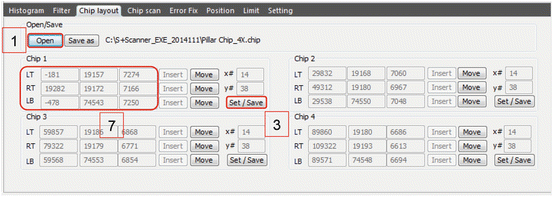
The display of the ‘Chip layout’ tool bar

-
2.
Select a desired chip file and click ‘Open’ in the window. For example, the layout of the micropillar chip at 4× magnification lens is selected (Fig. 6.17).
Fig. 6.17 
Window displaying the list of chip files

-
3.
To change the X, Y, and Z coordinates of the chips in the desired chip file, click ‘Set/Save’ button among four chips loaded (i.e., Chip 1, Chip 2, Chip 3, and Chip 4) (Fig. 6.16). Note: This will allow one to change the X, Y, and Z coordinates of LT, RT, and LB corners of the chip selected.
-
4.
To read accurate XYZ coordinates, click the ‘Axis’ icon in the ‘XYZ Move’ tab in ‘Home’ window to open the ‘Axis’ window (Fig. 6.18).
Fig. 6.18 
‘Home’ window showing the ‘Axis’ icon highlighted in red in the ‘XYZ Move’ tab

-
5.
In the ‘Live view’ tab, click the ‘Live’ icon to observe a real-time cell image. Note: We need to place three micropillars or microwells at the LT, RT, and LB corners in the center of the ROI.
-
6.
In the ‘Axis’ window (Fig. 6.19), increase/decrease X, Y, and Z coordinates by clicking the x+/x−, y+/y−, z+/z− buttons respectively to identify three micropillars or microwells at the LT, RT and LB corners of the chip. Note: The changes in the XYZ coordinates will be reflected immediately in the live image of cells.
Fig. 6.19 
The display of ‘Axis’ window

-
7.
Select the optimum XYZ coordinates at which the image is properly focused, and enter those coordinates in the ‘Chip layout’ tool bar (Fig. 6.16).
6.4 Summary
Imaging technology is the key determinant for a successful HCI assay. An ideal HCI system enables the user to acquire high-resolution images of fluorescently labeled cells at a high speed in real time. In this chapter, we introduced some commonly available HCI devices and provided simple procedures for acquiring high-content images in a high-throughput fashion from the micropillar/microwell chip platform using the S+ Scanner. These procedures can be further modified to acquire high-content images from traditional HTS platforms such as 96- and 384-well plates.
References
Buchser, W., Collins, M., Garyantes, T., Guha, R., Haney, S., Lemmon, V., et al. (2012). Assay development guidelines for image-based high content screening, high content analysis and high content imaging. In S. GS, C. NP, H. Nelson, M. Arkin, D. Auld, C. Austin, et al. (Eds.), Assay guidance manual. (pp. 1–69). Bethesda, MD: Eli Lilly & Company and the National Center for Advancing Translational Sciences.
Talbot, C. B., McGinty, J., Grant, D. M., McGhee, E. J., Owen, D. M., Zhang, W., et al. (2008). High speed unsupervised fluorescence lifetime imaging confocal multiwell plate reader for high content analysis. Journal of Biophotonics, 1(6), 514–521. doi:10.1002/jbio.200810054.
Celli, J. P., Rizvi, I., Blanden, A. R., Massodi, I., Gidden, M. D., Pogue, B. W., et al. (2014). An imaging-based platform for high-content, quantitative evaluation of therapeutic response in 3D tumour models. Scientific Reports. doi:10.1038/srep03751.
Romano, S. N., & Gorelick, D. A. (2014). Semi-automated imaging of tissue-specific fluorescence in Zebrafish Embryos. Journal of Visualized Experiments, 87, e51533. doi:10.3791/51533.
Bickle, M. (2010). The beautiful cell: High-content screening in drug discovery. Analytical and Bioanalytical Chemistry, 398, 219–226. doi:10.1007/s00216-010-3788-3.
Jahr, W., Schmid, B., Schmied, C., Fahrbach, F. O., & Huisken, J. (2015). Hyperspectral light sheet microscopy. Nature Communications, 6, 1–7. doi:10.1038/ncomms8990.
Reynaud, E. G., Peychl, J., Huisken, J., & Tomancak, P. (2015). Guide to light-sheet microscopy for adventurous biologists. Nature Methods, 12(1), 30–34. doi:10.1038/nmeth.3222.
Rae Chi, K. (2012). High on high content: A guide to some new and improved high-content screening systems. The Scientist Magazine, 1–7.
Starkuviene, V., & Pepperkok, R. (2007). The potential of high-content high-throughput microscopy in drug discovery. British Journal of Pharmacology, 152(1), 62–71. doi:10.1038/sj.bjp.0707346.
Author information
Authors and Affiliations
Editor information
Editors and Affiliations
Appendix
Appendix
In the S+ Scanner, the following four filter sets are installed.
-
1.
Multiband filter
Model (Semrock) | DA/FI/TR/Cy5-A-000 (Multi-band) |

http://www.semrock.com/SetDetails.aspx?id=2777
-
2.
Orange filter
Model (Semrock) | TxRed-4040C-000 (RED) |

http://www.semrock.com/SetDetails.aspx?id=2799
-
3.
Blue filter
Model (Semrock) | DAPI-5060C-000 (Blue) |

http://www.semrock.com/SetDetails.aspx?id=2779
-
4.
Green filter
Model (Omega) | XF404 (Green) |

Rights and permissions
Copyright information
© 2016 The Author(s)
About this chapter
Cite this chapter
Joshi, P., Yu, KN., Serbinowski, E., Lee, MY. (2016). 3D-Cultured Cell Image Acquisition. In: Lee, MY. (eds) Microarray Bioprinting Technology. Springer, Cham. https://doi.org/10.1007/978-3-319-46805-1_6
Download citation
DOI: https://doi.org/10.1007/978-3-319-46805-1_6
Published:
Publisher Name: Springer, Cham
Print ISBN: 978-3-319-46803-7
Online ISBN: 978-3-319-46805-1
eBook Packages: Biomedical and Life SciencesBiomedical and Life Sciences (R0)