
Abstract
Knowledge of basic circuit analysis
Access provided by Autonomous University of Puebla. Download chapter PDF
Keywords
- Field-effect transistor (FET)
- Metal-oxide semiconductor FET (MOSFET)
- Enhancement-mode MOSFET
- E-MOSFET
- Depletion-mode MOSFET
- n-channel MOSFET
- p-channel MOSFET
- NMOS transistor
- PMOS transistor
- MOSFET drain terminal
- MOSFET source terminal
- MOSFET gate terminal
- MOSFET body terminal
- MOSFET substrate terminal
- Four-terminal MOSFET
- Three-terminal MOSFET
- MOSFET channel
- MOSFET threshold voltage
- MOS capacitor
- Ideal MOS capacitor model
- Surface space-charge region of MOS capacitor
- Surface voltage of MOS capacitor
- Surface potential of MOS capacitor
- One-sided pn-junction approximation
- Strong inversion in MOS capacitor
- Inversion layer of MOS capacitor
- Flat-band voltage
- Work function difference
- Junction FET (JFET)
- Metal–semiconductor FET (MESFET)
- Triode region of a MOSFET
- Saturation region of a MOSFET
- Cutoff region of a MOSFET
- Process transconductance parameter
- MOSFET transconductance parameter
- MOSFET lumped process parameter
- MOSFET turn-on resistance
- Channel pinch-off
- Saturation current
- Saturation velocity
- Velocity saturation region
- Early effect
- Channel modulation effect
- Transconductance curve
- Large-signal MOSFET model in saturation
- MOSFET parameter extraction
- MOSFET on-state resistance
- MOSFET resistor-switch model
- CMOS logic gates
- CMOS NOT gate (inverter)
- CMOS NAND gate
- CMOS NOR gate
- Gate output resistance
- Method of assumed states
- Gate-bias (fixed-gate) MOSFET circuit
- Diode-connected MOSFET circuit
- Load-line analysis
- Load line
- Basic MOSFET actuator device
- Common-source MOSFET amplifier
- Voltage transfer characteristic
- Quiescent point of NMOS amplifier
- Small-signal MOSFET model
- Open-circuit small-signal voltage gain
- Small-signal MOSFET transconductance
- Small-signal ground
Prerequisites:
-
Knowledge of basic circuit analysis
-
Exposure to theory of the pn-junction (optional)
-
Exposure to BJT circuit analysis and amplifiers (Chapter 17, optional)
Objectives of Section 18.1:
-
Learn physical composition of the field-effect transistor, four- and three-terminal configurations
-
Understand principle of operation of the MOSFET
-
Realize the origin and understand the value of MOSFET threshold voltage
-
Be able to estimate threshold voltage based on MOSFET’s physical composition
Objectives of Section 18.2:
-
Learn MOSFET test circuits
-
Become familiar with the dynamics of channel inversion and quantify the underlying mechanism
-
Derive MOSFET equations (large-signal model) for three regions of operation from first principles
-
Pay special attention to large-signal MOSFET model in saturation
-
Become familiar with v-i dependencies for the NMOS and PMOS transistors
Objectives of Section 18.3:
-
Learn the resistor-switch model of the MOSFET for switching applications
-
Apply the resistor-switch model of the MOSFET to logic gates
-
Understand the value of the triode and cutoff regions for switching applications
-
Become fluent with the method of assumed states for MOSFET DC circuit analysis
-
Use the load-line method, either graphically or analytically
-
Solve in basic MOSFET DC bias circuits
Objectives of Section 18.4:
-
Learn circuit topology of the common-source MOSFET amplifier
-
Analyze and characterize the voltage transfer characteristic of the common-source amplifier
-
Understand the value of the saturation region for amplifier applications
-
Be able to properly select the quiescent (bias) point
-
Formulate the small-signal MOSFET model and solve in the common-source amplifier circuit
Application Examples:
-
Output resistance of digital logic gates
-
Basic MOSFET switching actuator
1 Principle of Operation and Threshold Voltage
In this chapter we study the field-effect transistor (FET). The most important member of the FET family is the metal-oxide-semiconductor FET or MOSFET. Similar to the npn and pnp BJT transistors, MOSFETs are subdivided into n-channel MOSFETs and p-channel MOSFETs, also known as NMOS and PMOS transistors. The abbreviation CMOS, or complementary MOS, implies an integrated circuit which incorporates both of these types of transistors on the same substrate. It is the CMOS transistor that allows high-density chip integration as part of microelectronic analog and digital circuits. MOSFETs are used in both logic gates and in memory cells. Discrete power MOSFETs are also deployed in many power engineering applications. We will concentrate on the enhancement-mode MOSFET (or E-MOSFET), which relies on a positive gate-to-source threshold voltage. Other MOSFET types ( depletion-mode MOSFET ) may have either negative or near-zero threshold voltages.
1.1 Physical Structure: Terminal Voltages and Currents
An enhancement-mode n-channel MOSFET (NMOS transistor) is a four-terminal semiconductor device. The NMOS transistor shown in Fig. 18.1 consists of a p-doped substrate (the Si wafer) into which two n (or rather heavily doped n+) regions, the source and the drain, are formed through ion implantation. The gate electrode (source of the control voltage) used to be a metal film, but nowadays it is a heavily doped polysilicon. The gate length L, also known as channel length, can be as small as 30 nm. The gate isolation, necessary to form a capacitor, is a SiO2 dielectric. It is formed directly from the Si substrate by thermal oxidation of Si. There are four metal electrodes corresponding to four transistor terminals: the gate terminal (G), the source terminal (S), the drain terminal (D), and the body (or substrate) terminal (B). The basic geometrical device parameters are the channel length, L, in horizontal direction, and the channel width, W, in vertical direction in Fig. 18.1. The channel length is the distance between the two pn+−junctions; the channel width characterizes the region of electron carrier flow between the drain and the source. Typical substrate acceptor concentrations (p-doping) are in the range of \( {N}_{\mathrm{A}}={10}^{16}-{10}^{17}\kern0.5em {\mathrm{cm}}^{-3} \). The doping of the two n+ domains (donor doping) is large. For example, \( {N}_{\mathrm{D}}\approx {10}^{19}\kern0.5em {\mathrm{cm}}^{-3} \) for a power MOSFET.

Semiconductor composition of the NMOS transistor—lateral or planar channel design. The vertical channel design typical for power MOSFETs implies rotation by 90 degrees
The circuit symbol for the four-terminal NMOS transistor is shown in Fig. 18.2a. The device is strictly symmetrical, which means that we can interchange the drain and the source; this is in contrast to the BJT . The arrow denotes the pn-junction polarity (from p to n) similar to the diode arrow. The four-terminal NMOS transistor is widely used in integrated circuits . In discrete circuits, which employ discrete transistor components, the body terminal is tied to the source terminal as shown in Fig. 18.1b. Therefore, the NMOS transistor becomes the three- terminal MOSFET device (gate, drain, and source), similar to the BJT. However, it is no longer symmetrical. Figure 18.2b shows the corresponding circuit symbol. You encounter this symbol in the majority of manufacturer datasheets and electronic simulation packages. Simplified symbols are widely used; see Fig. 18.2c.

Circuit symbols of (a) a four-terminal NMOS transistor, (b) a three-terminal asymmetric NMOS transistor with the body tied to the source, and (c) the same device but simplified
We are going to study only the three-terminal configuration and use the symbol shown in Fig. 18.2b. Figure 18.3a shows transistor terminal voltages for the three-terminal device:

Terminal voltages and currents for the NMOS transistor
-
Gate-source voltage υ GS
-
Drain-source voltage υ DS
-
Gate-drain voltage υ GD
Only two voltages are independent since KVL relates all three voltages to each other. The voltages υ GS and υ DS are chosen as independent variables. Then,
The principal difference from the BJT is that the control terminal of the transistor, the gate, is electrically insulated. There is no current flowing into or out of the gate. Therefore, the transistor current is the only drain current, i D, which flows from the drain to the source in Fig. 18.3b.
Exercise 18.1
A NMOS transistor has the gate-source voltage of 2 V and drain-source voltage of 0.3 V. What is the gate-drain voltage?
Answer: 1.7 V.
1.2 Simplified Principle of Operation
We consider thesimplified transistor circuit shown in Fig. 18.4. Both the source and the substrate are grounded. When \( {\upsilon}_{\mathrm{GS}}=0 \), the path between the drain and the source includes two oppositely directed pn-junction diodes; see Fig. 18.4a. Therefore, there will be no current between the drain and the source for any possible value of drain-source voltage υ DS since one of the diodes will always be off. Now let us assume a positive control voltage υ GS is applied to the gate control terminal and \( {\upsilon}_{\mathrm{DS}}=0 \) for simplicity. A capacitor will form between the gate and all remaining (grounded) terminals; the initial electric field is shown in Fig. 18.4b by dashed lines. This electric field attracts more negative electron carriers to the channel between the drain and the source and repels the positive carrier (holes) from the channel until the initial electric field will be essentially neutralized in the bulk of the substrate. The dependence of the electron concentration in the channel on υ GS is exponential, i.e., very sharp. When υ GS reaches a certain threshold value V Th or exceeds it, the MOSFET channel appears (a thin subsurface domain just below the oxide) that has enough electron carriers to form a conducting “wire” between the drain and source as in Fig. 18.4b. The transistor switch becomes closed and transistor conducts the current i D from the drain to the source given any (even small) positive voltage \( {\upsilon}_{\mathrm{DS}}>0 \). One may think of the boundary of the n+ region in Fig. 18.4b as a “rubber band” that is pushed away from the gate by the positive gate voltage. The value V Th is the intrinsic threshold voltage (or simply threshold voltage) of the NMOS transistor. V Th depends on transistor geometry and its doping concentrations. For the NMOS transistor, the threshold voltage is often denoted by V Tn and for the PMOS transistor by V Tp. In the following text, we will attempt to keep the generic notation V Th for both transistor types.

Simplified NMOS configuration and creating a channel for current flow
1.3 NMOS Capacitor
The phenomenon described above is known as channel inversion (from p- to n-type) of the NMOS transistor. The inversion can be quantified analytically since we deal with a homogeneous p-type material in the bulk of the channel, as you can see in Fig. 18.4b. The central region of the NMOS transistor in Fig. 18.4 thus forms a MOS capacitor that consists of the gate, i nsulator, and the p-body. We will apply the semiconductor analysis to the MOS capacitor and use its one-dimensional electrostatic model which is shown in Fig. 18.5a (in fact it is turned 90° counterclockwise with respect to Fig. 18.4).

(a) Central region of the MOSFET under an applied voltage υ GS: the MOS capacitor. (b) to (d) Formation of the depletion and inversion layers in the substrate. The entire region close to the semiconductor surface is called the surface space-charge region
The ideal MOS capacitor model will be considered first. By KVL, the voltage \( {\upsilon}_{\mathrm{GS}}>0 \) is the sum of two positive components shown in Fig. 18.5a:
The first component V S is the voltage across the semiconductor substrate, which is also called the surface voltage or the surface potential \( {\varphi}_{\mathrm{S}}={V}_{\mathrm{S}} \) (given zero potential at the body terminal). The second component V OX is the voltage across the oxide layer. We will express it in terms of the surface potential \( {\varphi}_{\mathrm{S}}={V}_{\mathrm{S}} \) first. Then, φ S itself will be quantified at the onset of strong inversion. Substitution of those two values in Eq. (18.2) will give us the desired threshold voltage V Tn. The corresponding analysis relies upon semiconductor surface physics and may be skipped if necessary.
1.4 Voltage Across the Oxide Layer Before and at the Onset of Strong Inversion
At any \( {\upsilon}_{\mathrm{GS}}>0 \), the surface voltage is also positive, i.e., \( {V}_{\mathrm{S}}>0 \). The corresponding electric field directed into the body will push the positive holes into the depth of the substrate and leave immovable negative ions behind; this is seen in Fig. 18.5b–d. Hence, a depletion layer will be formed, similar to the pn-junction depletion layer . Assume that the body is uniformly doped and has an acceptor concentration \( {N}_{\mathrm{A}}>>{n}_i \) where n i is the intrinsic concentration of holes and electrons, \( {n}_i\approx 1\times {10}^{10}\kern0.5em {\mathrm{cm}}^{-3} \) for Si. The depletion layer is nearly the abrupt region of a uniform negative ion concentration N A and the width W d. The depletion layer width W d may be found analytically as
Here, ε is the dielectric constant of the substrate; in Si, \( \varepsilon =1.05\times {10}^{-12}\mathrm{F}/\mathrm{cm} \). The total charge Q of the depletion layer per unit surface (units of C/cm2) is subsequently given by
This is the negative charge on one side of the oxide capacitor with capacitance C OX per unit area. The charge on the opposite side (gate) must be positive and of the same absolute value in order to keep the device electrically neutral. The voltage of the oxide capacitor is therefore
where the dielectric constant of the SiO2 oxide is \( {\varepsilon}_{\mathrm{OX}}=3.45\times {10}^{-13}\mathrm{F}/\mathrm{cm} \) and t OX is the oxide thickness.
Example 18.1
Given \( {V}_{\mathrm{S}}=1\kern0.5em \mathrm{V} \) and \( {N}_{\mathrm{A}}=5\times {10}^{16}\kern0.5em {\mathrm{cm}}^{-3} \) estimate the voltage across the SiO2 oxide layer with a thickness of 4 nm; the NMOS body is Si.
Solution: We will use centimeters as length units in accordance with generally accepted semiconductor convention. The oxide-layer capacitance is given by
Substitution into Eq. (18.5) yields
1.5 Voltage Across the Semiconductor Body
At any υ GS, the MOS capacitor is still a system in equilibrium (no currents of any kind) as long as υ DS is zero. Then, the electron and hole concentrations n(x) and p(x) are
The last expression in Eq. (18.8) is the mass-action law of a semiconductor. When a positive voltage υ GS is applied, an electric field is established in the p-doped material which is the negative spatial derivative of the potential distribution φ(x); see Fig. 18.5a. The concentrations are modified by the potential φ(x). Since the potential is defined to within a constant, one can select this constant in order to satisfy Eq. (18.8) deep in the body when \( \varphi (x)=0 \). Equation (18.8) is therefore transformed to
where V T is the thermal voltage. The boundary condition at \( x=0 \) is simply \( \varphi (x)={\varphi}_s={V}_S \). At the boundary of the semiconductor, i.e., at \( x=0 \), we obtain
It is a common agreement to choose the onset of strong inversion as a surface voltage at which the electron charge concentration n reaches N A at the boundary of the semiconductor; this is depicted in Fig. 18.5c. Thus, the surface charge concentration is inverted from \( p={N}_{\mathrm{A}} \) with no applied voltage to \( n={N}_{\mathrm{A}} \) when the channel inversion starts. From Eq. (18.10), the surface voltage becomes
where the voltage constant \( {\varphi}_{\mathrm{F}}={V}_{\mathrm{T}}\ \ln\ {N}_{\mathrm{A}}/{n}_i \) is known as the Fermi potential of the semiconductor. We emphasize that at the onset of strong inversion the total charge Q of the depletion layer per unit surface given by Eq. (18.4) is still much greater than an extra free electron charge brought close to the surface. This is because the surface concentration \( n={N}_{\mathrm{A}} \) very quickly decreases when the distance from the surface increases.
Exercise 18.2
Given \( {N}_{\mathrm{A}}=5\times {10}^{16}\kern0.5em {\mathrm{cm}}^{-3} \) estimate surface voltage at the onset of strong inversion at room temperature of 25 °C. The NMOS transistor body is Si.
Answer: \( {V}_{\mathrm{S}}=0.79\kern0.5em \mathrm{V} \)
When V S continues to increase even slightly above the value predicted by Eq. (18.11), the surface electron concentration rises exponentially according to Eq. (18.10), and a rich n+ electron channel (or the inversion layer ) is quickly formed as illustrated in Fig. 18.5d. When strong inversion takes place, the depletion layer width W d no longer increases because the inversion layer starts blocking the electric field. Its maximum value is given by Eq. (18.3) with \( {V}_{\mathrm{S}}=2{\varphi}_{\mathrm{F}} \). A critical distinction between the NMOS capacitor and the NMOS transistor is the channel formation time. While for an NMOS capacitor it can take minutes to collect the necessary electrons from the p-doped semiconductor with few free electrons, the inversion electrons for the transistor are readily available from two nearby n+ regions—the source and the drain.
1.6 Threshold Voltage
The threshold voltage V Th of an NMOS transistor is defined as the gate-source voltage (18.2) at the onset of strong inversion when \( {V}_{\mathrm{S}}=2{\varphi}_{\mathrm{B}} \) according to Eq. (18.11). V OX still follows Eq. (18.5). Therefore,
The new extra term V FB on the right-hand side of Eq. (18.12) is called the flat-band voltage of the MOS capacitor. This term is needed for two reasons. The somewhat less important one is the presence of charges in the oxide layer due to ionic contamination. The second, important reason is the built-in voltage or potential of a boundary between two materials. This effect is similar to the built-in potential or voltage of the pn-junction. The built-in voltages of the metal-oxide boundary and of the semiconductor-oxide boundary do not cancel each other; the corresponding v oltage difference is known as a work function difference ψ GS between the gate and the semiconductor; it appears across the oxide layer (Fig. 18.6). Without going into further details, we may assume \( {V}_{\mathrm{FB}}\approx {\psi}_{\mathrm{GS}} \) and write

Work function difference ψ GS as a function of body doping for gate electrodes of polysilicon and aluminum, respectively, on a p-Si body of an NMOS transistor
Example 18.2
Estimate the threshold voltage V Th for a Si NMOS transistor with aluminum gate, \( {N}_{\mathrm{A}}=1\times {10}^{17}\kern0.5em {\mathrm{cm}}^{-3} \), and the SiO2 oxide layer with the thickness of 50 nm at room temperature of 25 °C.
Solution: We will use centimeters as length units in accordance with standard semiconductor convention. The surface voltage at the onset of strong inversion is given by Eq. (18.11), i.e.,
The oxide-layer capacitance and oxide voltage are given by Eq. (18.5), that is,
Finally, we find \( {\psi}_{\mathrm{GS}}=-0.94\kern0.5em \mathrm{V} \) from Eq. (18.13) and substitute all three contributions into the expression for the threshold voltage, \( {V}_{\mathrm{Th}}={\psi}_{\mathrm{GS}}+{V}_{\mathrm{S}}+{V}_{\mathrm{OX}} \). The result has the form \( {V}_{\mathrm{Th}}=2.31\kern0.5em \mathrm{V} \).
It is possible to extend the method of Example 18.2 to arbitrary values of oxide thickness t OX and body doping concentration N A. The result is shown in Fig. 18.7 where the threshold voltage is plotted as a function of N A and t OX. When the threshold voltage is positive (heavy body doping), the NMOS transistor is the enhancement-mode device (E-MOSFET). At light doping and small oxide thickness, the threshold voltage becomes negative. For different enhancement-mode MOSFETs, the V Th values vary in the range

Threshold voltage as a function of N A and t OX (Al gate)
Many different methods e xist to measure the threshold voltage. In practice, the threshold voltage is defined as a voltage when the drain current reaches a certain specified value.
1.7 PMOS Transistor
For a PMOS transistor (p-channel MOSFET ), all doping concentrations in Figs. 18.1 and 18.4 are reversed. The substrate is now of n-type, and the source and drain are heavily doped p+ regions. Consequently, all voltage polarities are reversed relative to their counterparts in the NMOS case. The PMOS and NMOS transistors are two complementary devices. Figure 18.8 shows the circuit symbols for the PMOS transistor. We put the source on top in accordance with a more positive voltage applied to it.

Circuit symbols of (a) a four-terminal PMOS transistor, (b) a three-terminal asymmetric PMOS transistor with the body tied to the source, and (c) the same but simplified symbol
The threshold voltage between the gate and the source also becomes negative. Specifically, Eq. (18.12) for the PMOS transistor is modified as
where \( {V}_{\mathrm{FB}}\approx {\psi}_{\mathrm{GS}} \) and ψ GS is given by two upper curves in Fig. 18.6.
Exercise 18.3
In Example 18.2, invert all doping concentrations and find the threshold voltage of the corresponding PMOS transistor.
Answer: \( {V}_{\mathrm{Th}}\approx -3.3\kern0.5em \mathrm{V} \).
1.8 Oxide Thicknesses and Capacitances in CMOS Processes
MOSFETs used in integrated circuits are fabricated in a number of CMOS processes. Each process is characterized by the minimum channel length L as seen in Fig. 18.1. Smaller lengths allow us to pack a greater number of transistors per unit area. The CMOS design is constantly evolving so as to decrease the channel length. Table 18.1 lists some CMOS device parameters: oxide layer thickness and oxide capacitance used in the design of analog ICs. This information helps to find the threshold voltages of the transistors.
1.9 Family Tree of FETs
The MOSFET is not the only member of the field-effect transistor family. In contrast to the BJT, this device family is extensive. Figure 18.9 lists three examples. Let us first discuss the idea of W. Shockley (1952) for the junction FET (JFET) . We can use a depletion region of the reverse-biased pn-junction to control, i.e., reduce or increase, the net channel opening b between the drain and the source in Fig. 18.10a. This is the JFET composition. When current flows from the drain to the source, the device becomes a voltage-controlled resistor, with the control voltage being the reverse-bias voltage of the pn-junction. Indeed there is still no gate current since the reverse-biased pn-junction is a very good insulator. A similar situation applies for the MESFET (metal–semiconductor FET ) in Fig. 18.10b. However, here the origin of the depletion layer is different, i.e., the metal–semiconductor interface and the corresponding Schottky potential barrier. MESFETs constructed with Si, and especially gallium arsenide (GaAs), are typically used in RF power amplifiers. Many additional FET types exist or are still awaiting discovery.

Modifications of the field-effect transistor involving different types of gates

Two schematic FET configurations: (a) n-channel JFET and (b) n-channel MESFET. A variant for both configurations is the dual gate arrangement. You should note that the corresponding circuit symbols have a continuous gate, denoting the normally “on” state
2 Theoretical Model of a MOSFET
2.1 Test Circuit and Operating Regions
Figure 18.11 shows the test circuit for the three-terminal NMOS transistor. Gate-source voltage υ GS and drain-source voltage υ DS are varied. The drain current i D is measured at every particular voltage combination. Our goal is to derive analytical expressions for the drain current i D. The analytical models described below rely on the corresponding measured data, which have been obtained with circuits similar to that in Fig. 18.11.

Schematic diagram of the NMOS transistor test circuit
The NMOS (and PMOS) transistor has three operating regions: triode, saturation, and cutoff listed in Table 18.2. All three regions are used. Most common MOSFET switching circuits like logic gates utilize the cutoff and triode regions in order to characterize two binary steady states—logic 0 and 1. However, during the fast transition between the states, the transistors enter the saturation region. MOSFET amplifier circuits solely utilize the saturation region of operation.
The regions of operation are determined by the value of υ DS as compared to the control voltage υ GS. The triode region starts with a linear (or ohmic) subregion . Table 18.2 indicates one more useful voltage parameter: the overdrive voltage \( {\upsilon}_{\mathrm{OV}}={\upsilon}_{\mathrm{GS}}-{V}_{\mathrm{Th}} \). The NMOS transistor typically operates at large overdrive voltages.
2.2 Linear Subregion of Triode Region at Strong Inversion
Let us consider a situation when a large enough gate voltage (typically significantly larger than V Th) is applied to induce the inversion layer between the drain and the source. The cross section of the NMOS transistor is shown in Fig. 18.12. This is a two-dimensional structure. For the analytical description, the electric field is conveniently subdivided into two components: one is in the horizontal direction from gate to body termination, and the other is in the vertical direction from drain to source. Henceforth, two sets of associated voltages (potentials) should describe the 2D models. We analyze fields and voltages in the horizontal direction first.

Voltage distribution across the channel in the triode region. The linear charge and voltage profiles in Fig. 18.12b are an approximation
When the drain is at zero volts or at a small positive voltage with respect to the source (body), the gate-source voltage appears to be nearly uniform in space along the length of the channel L; this is seen in Fig. 18.12a. The charge density in the inversion layer per unit area Q INV measured in C/cm2 is also uniform when the distance x along the channel changes. To find Q INV the following observation is made. The threshold voltage V Th is responsible for creating the depletion layer in the semiconductor body at the onset of strong inversion. Any excess or overdrive voltage \( {\upsilon}_{\mathrm{OV}}=\left({\upsilon}_{\mathrm{GS}}-{V}_{\mathrm{Th}}\right) \) thus controls Q INV in the inversion layer since the depletion layer parameters no longer change. Q INV is the negative charge on one side of the oxide capacitor with capacitance C OX per unit area. The charge on the opposite side (gate) must be positive and of the same absolute value in order to keep the device electrically neutral. Therefore,
We now turn to the vertical fields. The drain current i D in Fig. 18.12 is the motion of charge Q INV with speed \( \upsilon ={\mu}_{\mathrm{ns}}E \) in the (vertical) constant electric field \( E={\upsilon}_{\mathrm{DS}}/L \) where μ ns is the electron surface mobility ; \( {\mu}_{\mathrm{ns}}\approx 450\;{\mathrm{cm}}^2/\left(\mathrm{V}\cdot \mathrm{s}\right) \) or less. The drain current that flows from drain to source is thus given by (W is the channel width)
The constant k ′ n with units of A/V2 (more often mA/V2) is called the process transconductance parameter . The name implies that it is determined by the particular fabrication technology. The constant \( {k}_n=\left(W/L\right){k}_n^{\prime } \) with the same units is the MOSFET transconductance parameter (also called the lumped process parameter ); it also includes information about the gate dimensions. Typically, k n is on order of 1 mA per V2 or less for small-signal MOSFET transistors. For power MOSFETs, however, it can be much larger: on the order of 100 mA per V2. Equation (18.16) states that at small positive υ DS the NMOS transistor behaves like a linear resistance r DS, which is controlled by the gate-source voltage,
The resistance r DS can be measured in the laboratory. It is also called the turn-on resistance . This resistance of a MOSFET is a key parameter that is typically specified in the manufacturer’s datasheets (in contrast to k n ).
2.3 Nonlinear Subregion of Triode Region at Strong Inversion
When υ DS increases (but still remains less than \( {\upsilon}_{\mathrm{GS}}-{V}_{\mathrm{Th}} \)), the situation depicted in Fig. 18.12b is observed. Close to the source region, the gate still “sees” the absolute source voltage (0 V in this case) as the terminal voltage. However, close to the drain, the gate does not “see” 0 V, but sees the drain voltage as the terminal voltage. The resulting voltage becomes \( {\upsilon}_{\mathrm{GD}}={\upsilon}_{\mathrm{GS}}-{\upsilon}_{\mathrm{DS}} \). Therefore, a variable gate-source voltage υ GS(x) is effectively applied across the channel. The tip of the inversion layer becomes thinner, which is schematically shown in Fig. 18.12b. Introducing an as-yet unknown channel voltage profile y(x), we have
Consequently, the charge of the inversion layer given by Eq. (18.15) also becomes a function of x as illustrated in Fig. 18.12b:
The vertical potential electric field in the channel is now variable too, that is,
Next, the current along the inversion layer, \( {i}_{\mathrm{D}}=-W{Q}_{\mathrm{INV}}\upsilon \), becomes
By KCL, the current along the inversion layer must remain constant. If this condition is enforced, Eq. (18.18c) becomes a nonlinear ODE augmented with the boundary conditions Eq. (18.18a). It allows us to find the voltage profile y(x) along the channel analytically. The corresponding solution has the form (the proof is suggested as one of the homework problems)
The profile y(x) is quite linear (\( \approx x/L \)) everywhere in the channel at small υ DS and close to the source for any υ DS, but it becomes steeper when approaching the drain at large υ DS. Since all channel parameters are now defined, the transistor current can be calculated by picking up any point along the channel. An alternative and more common approach is to integrate Eq. (18.18d) from x to L and use boundary conditions Eq. (18.18a) along with the constant-current condition. Either method gives the simple final expression for the drain current in the form:
Equation (18.19) reveals a nonlinear (parabolic) dependence of i D on υ DS; this is an exact result. We could still use Eq. (18.17) too. However, r DS is no longer constant; it becomes voltage dependent, i.e.,
and increases with increasing υ DS. When the drain-source voltage υ DS is small compared to \( {\upsilon}_{\mathrm{GS}}-{V}_{\mathrm{Th}} \), the nonlinear MOSFET model is reduced to a linear one. Equation (18.19) becomes asymptotically equivalent to Eq. (18.16), and Eq. (18.20) reduces to Eq. (18.17).
2.4 Saturation Region
As υ DS continues to increase and eventually reach \( {\upsilon}_{\mathrm{GS}}-{V}_{\mathrm{Th}} \), the tip of the inversion layer in Fig. 18.12b becomes infinitely thin since the inversion layer charge in Eq. (18.18b) is exactly zero at \( x=L \). This effect is known as the channel pinch-off . It determines entering the saturation region of a MOSFET. The terminal drain current ( saturation current ) is found from Eq. (18.19) to be
This corresponding drain-source voltage is known as the drain saturation voltage:
While the MOSFET model correctly estimates the saturation voltage and the saturation current, it has one major drawback: the finite current at zero inversion charge would imply infinite carrier velocity. This contradiction has its roots in semiconductor physics. Figure 18.13 provides an explanation. The carrier velocity in a semiconductor cannot exceed a certain value \( \upsilon \le {\upsilon}_{\mathrm{sat}} \), which is known as the saturation velocity . An excess electric field (or voltage) applied to accelerate carriers even further will result in the generation of certain optical phonons (atom vibrations that light) and the loss of extra kinetic energy. Thus, the artificial carrier-free pinch-off region is in fact a small velocity saturation region that appears near the drain in Fig. 18.13.

Channel behavior at saturation voltage and beyond and voltage drops across the respective channel areas. The charge profile is an exact nonlinear solution of Eq. (18.18)
The model of the MOSFET in saturation shown in Fig. 18.13 is quantified as follows. A portion of υ DS equal to the overdrive voltage, \( {\upsilon}_{\mathrm{GS}}-{V}_{\mathrm{Th}} \), is spent to create the tapered channel with the saturation drain current given by Eq. (18.21a). At the end of this channel, we enter the velocity saturation region. Any excess portion of υ DS is applied solely to the velocity saturation region. However, such an excess voltage does not change the inversion charge in this region:
since the carrier velocity is fixed at υ sat. Instead, the electric field energy is transformed into lattice vibrations. An important conclusion is that the drain current does not change either with increasing υ DS above the overdrive voltage, \( {\upsilon}_{\mathrm{GS}}-{V}_{\mathrm{Th}} \). It remains equal to i Dsat from Eq. (18.21a).
2.5 The v-i Dependencies
Table 18.3 summarizes the simple yet accurate model of the NMOS transistor established in this section.
Example 18.3
A NMOS transistor has the following parameters: \( {V}_{\mathrm{Th}}=2\kern0.5em \mathrm{V} \) and \( {k}_n=3\kern0.5em \mathrm{m}\mathrm{A}/{\mathrm{V}}^2 \). Plot the drain current for source-drain voltages from the interval \( {\upsilon}_{\mathrm{DS}}=\left[0 - 9\right]\kern0.5em \mathrm{V} \) and at three values of the gate-source voltage \( {\upsilon}_{\mathrm{GS}}=3,\kern0.5em 4,\kern0.5em \mathrm{and}\kern0.5em 5\kern0.5em \mathrm{V} \) on the same figure.
Solution: We determine the saturation voltages first. According to the definition, \( {\upsilon}_{\mathrm{DSsat}}={\upsilon}_{\mathrm{GS}}-{V}_{\mathrm{Th}}=1,\kern0.5em 2,\kern0.5em \mathrm{and}\kern0.5em 3\kern0.5em \mathrm{V} \). Below these voltages, the triode model Eq. (18.23a) is used. It results in a parabola, whose top point is exactly at the saturation voltage. Above those voltages, the current remains constant; it is equal to the saturation current from Eq. (18.23b). The corresponding values are \( {i}_{\mathrm{DGS}}=1.5,\kern0.5em 6,\kern0.5em \mathrm{and}\kern0.5em 13.5\kern0.5em \mathrm{m}\mathrm{A} \). The result is shown in Fig. 18.14a. Note that the boundary between the two regions (triode and saturation) is another parabola:

(a) Drain current as a function of the drain-source voltage for an NMOS transistor with \( {V}_{\mathrm{Th}}=2\kern0.5em \mathrm{V} \) and \( {k}_n=3\kern0.5em \mathrm{m}\mathrm{A}/{\mathrm{V}}^2 \). (b) Drain current as a function of the source-drain voltage for a PMOS transistor with \( \left|{V}_{\mathrm{Th}}\right|=2\kern0.5em \mathrm{V} \) and \( {k}_{\mathrm{p}}=3\kern0.5em \mathrm{m}\mathrm{A}/{\mathrm{V}}^2 \)
Also note the linear subregion of the triode region at small drain-source voltages.
Example 18.4
An enhancement-mode NMOS transistor is characterized by \( {k}_n=4\kern0.5em \mathrm{m}\mathrm{A}/{\mathrm{V}}^2 \). For a given set of bias voltages, determine the region of operation and calculate the transistor’s drain current:
-
A.
\( {\upsilon}_{\mathrm{GS}}=3\kern0.5em \mathrm{V},\ {\upsilon}_{\mathrm{DS}}=10\kern0.5em \mathrm{V},\ \mathrm{and}\kern0.5em {V}_{\mathrm{Th}}=2\kern0.5em \mathrm{V}. \)
-
B.
\( {\upsilon}_{\mathrm{GS}}=-2\kern0.5em \mathrm{V},\ {\upsilon}_{\mathrm{DS}}=10\kern0.5em \mathrm{V},\ \mathrm{and}\kern0.5em {V}_{\mathrm{Th}}=1\kern0.5em \mathrm{V}. \)
-
C.
\( {\upsilon}_{\mathrm{GS}}=3\kern0.5em \mathrm{V},\ {\upsilon}_{\mathrm{DS}}=2\kern0.5em \mathrm{V},\ \mathrm{and}\kern0.5em {V}_{\mathrm{Th}}=2\kern0.5em \mathrm{V}. \)
-
D.
\( {\upsilon}_{\mathrm{GS}}=3\kern0.5em \mathrm{V},\ {\upsilon}_{\mathrm{DS}}=0.5\kern0.5em \mathrm{V},\ \mathrm{and}\kern0.5em {V}_{\mathrm{Th}}=2\kern0.5em \mathrm{V}. \)
Solution: We inspect the inequalities from Table 18.3. Case A then corresponds to saturation, Case B to cutoff (irrespective of drain-to-source voltage), Case C to saturation, and Case D corresponds to the triode region. The transistor current (drain current i D) is given by Eq. (18.23). Therefore, one has
A \( {i}_{\mathrm{D}}=2\ \mathrm{m}\mathrm{A} \), B \( {i}_{\mathrm{D}}=0\ \mathrm{m}\mathrm{A} \), C \( {i}_{\mathrm{D}}=2\ \mathrm{m}\mathrm{A} \), and D \( {i}_{\mathrm{D}}=1.5\ \mathrm{m}\mathrm{A} \).
Exercise 18.4
For the circuit of Fig. 18.11, determine the region of MOSFET operation as well as the drain current i D for each set of conditions given. Assume \( {k}_n=90\kern0.5em \mathrm{m}\mathrm{A}/{\mathrm{V}}^2 \) and \( {V}_{\mathrm{Th}}=2\kern0.5em \mathrm{V} \) for the general-purpose 2 N7000 MOSFET.
-
A.
\( {\upsilon}_{\mathrm{GS}}=4.5\kern0.5em \mathrm{V},\ {\upsilon}_{\mathrm{DS}}=2\kern0.5em \mathrm{V}. \)
-
B.
\( {\upsilon}_{\mathrm{GS}}=4.5\kern0.5em \mathrm{V},\ {\upsilon}_{\mathrm{DS}}=8\kern0.5em \mathrm{V}. \)
-
C.
\( {\upsilon}_{\mathrm{GS}}=1.5\kern0.5em \mathrm{V},\ {\upsilon}_{\mathrm{DS}}=8\kern0.5em \mathrm{V}. \)
Answer: A) Triode, i D =270 mA. B) Saturation, i D = 281 mA. C) Cutoff, i D = 0.
2.6 PMOS Transistor
A similar analysis can be repeated for the PMOS transistor with inverted doping concentrations. Table 18.4 summarizes the model of the PMOS transistor. The corresponding test circuit is shown in Fig. 18.15. Note that the |V Th| is used since V Th itself is negative. Also note that υ SG and υ SD are both positive. Table 18.4 is identical to Table 18.3 to within the substitutions \( {\upsilon}_{\mathrm{GS}}\to {\upsilon}_{\mathrm{SG}} \), \( {\upsilon}_{\mathrm{DS}}\to {\upsilon}_{\mathrm{SD}} \), and \( \left|{V}_{\mathrm{Th}}\right|\to {V}_{\mathrm{Th}} \).

Schematic diagram of the PMOS transistor test circuit
Exercise 18.5
Solve Example 18.3 for the PMOS transistor with \( \left|{V}_{\mathrm{Th}}\right|=2\kern0.5em \mathrm{V} \), \( {k}_{\mathrm{p}}=3\kern0.5em \mathrm{m}\mathrm{A}/{\mathrm{V}}^2 \), and \( {\upsilon}_{\mathrm{SG}}=3,\kern0.5em 4,\kern0.5em \mathrm{and}\kern0.5em 5\kern0.5em \mathrm{V} \).
Answer: The solution is shown in Fig. 18.14b.
2.7 Large-Signal MOSFET Model in Saturation
The saturation region of a MOSFET is important for amplifier applications and for fast digital switching circuits . Consider the NMOS transistor: according to Table 18.3, the transistor behaves as a constant-current source in the saturation region for any value of \( {\upsilon}_{\mathrm{DS}}>{\upsilon}_{\mathrm{GS}}-{V}_{\mathrm{Th}} \). However, if the gate-source voltage υ GS is now varied, the MOSFET becomes a voltage-controlled current source with respect to υ GS, as long as it remains in the saturation region. The corresponding result is given by Eq. (18.23b), which is valid for \( {\upsilon}_{\mathrm{DS}}>{\upsilon}_{\mathrm{GS}}-{V}_{\mathrm{Th}} \) and \( {\upsilon}_{\mathrm{GS}}>{V}_{\mathrm{Th}} \). This is a parabolic dependence. Figure 18.16 illustrates its behavior for \( {k}_{\mathrm{p}}=90\kern0.5em \mathrm{m}\mathrm{A}/{\mathrm{V}}^2 \) and a threshold voltage of 2 V. The parabola in Fig. 18.16 is known as the transconductance curve of the MOSFET, which expresses the output current i D in terms of υ GS. The transconductance curve terminates at \( {\upsilon}_{\mathrm{GS}}={V}_{\mathrm{Th}} \).

Transconductance curve of the NMOS transistor (i D versus υ GS)
Figure 18.17 shows the equivalent circuit representation of the NMOS transistor in the saturation region. The voltage-controlled nonlinear current source is described by the dependence \( {i}_{\mathrm{D}}=\frac{1}{2}{k}_n{\left({\upsilon}_{\mathrm{GS}}-{V}_{\mathrm{Th}}\right)}^2 \). This is the large-signal MOSFET model in saturation, which is valid for any values of υ GS and i D, both under DC and AC conditions. A similar model is established for the PMOS transistor.

MOSFET large-signal (nonlinear) current source model
2.8 Device Parameters in CMOS Processes
In order to determine the MOSFET model, we need to know the MOSFET transconductance parameter k n or k p. Their values are determined by oxide capacitance C OX and electron/hole surface mobility μ ns/ μ ps, along with gate dimensions L and W. Table 18.5 is an extension of Table 18.1; it provides the corresponding information for CMOS processes used in the design of analog ICs. This information may be used to find the corresponding transconductance parameter (the lumped process parameter).
3 MOSFET Switching and Bias Circuits
All problems in this section assume DC steady-state analysis. This is also valid for digital switching circuits where we will ignore the transition region between the two stable states. Still, transistor terminal voltages and drain current (in contrast to the supply voltages) will be denoted by small letters to emphasize that many results of this section are also applicable to the variable signals, either in the exact form or approximately.
3.1 Triode Region for Switching Circuits: Device Parameter Extraction
3.1.1 Turn-On Resistance and Its Behavior
Consider switching applications where values of υ DS are expected to be near 0 V and much less than the overdrive voltage \( {\upsilon}_{\mathrm{GS}}-{V}_{\mathrm{Th}} \). In this case, the v-i characteristic of the MOSFET belongs to the linear subregion of the triode region; this is seen in Fig. 18.18. Therefore, the MOSFET is modeled as a DC resistance (turn-on resistance), r DS.

MOSFET turn-on resistance r DS and its dependence on gate-source voltage for a 2 N7000 NMOS device
The value of this resistance is easily found by finding the slope of the \( {\upsilon}_{\mathrm{D}\mathrm{S}}-{i}_{\mathrm{D}} \) characteristic at the origin and inverting the result. It is given by Eq. (18.17) of the previous section, i.e.,
Example 18.5
A general-purpose 2N7000 NMOS transistor has the lumped process parameter \( {k}_n=90\kern0.5em \mathrm{m}\mathrm{A}/{\mathrm{V}}^2 \) and a threshold voltage of 2.0 V. The gate-source voltage is 5 V. Plot the drain current for drain-source voltages over the interval \( {\upsilon}_{\mathrm{DS}}=\left[0 - 9\right]\kern0.5em \mathrm{V} \) and determine the MOSFET’s turn-on resistance.
Solution: We determine the saturation voltage first. According to the definition, \( {\upsilon}_{\mathrm{DSsat}}={\upsilon}_{\mathrm{GS}}-{V}_{\mathrm{Th}}=\kern0.5em 3\kern0.5em \mathrm{V} \). Below this voltage the triode model Eq. (18.23a) is used; above this voltage the saturation model Eq. (18.23b) applies, that is,
The result is shown in Fig. 18.18a. The turn-on resistance from Eq. (18.26) is r DS = 3.7 Ω.
It is important to emphasize the turn-on resistance has a strong dependence on the gate-source voltage, as seen in Fig. 18.18b. Higher υ GS (higher overdrive voltages) lead to smaller resistances, which is usually desirable. The MOSFET turn-on resistance r DS is typically plotted as a function of υ GS for quick reference in specification sheets. Often, a logarithmic scale plots the resistance.
Exercise 18.5
Using the data of the previous example, plot r DS as a function of υ GS.
Answer: The plot is given in Fig. 18.18b. The threshold voltage is clearly seen.
3.1.2 Device Parameter Extraction
Although most MOSFET specification sheets provide values for V Th, most do not give values for the lumped process parameter k n . Therefore, one convenient method of determining the threshold voltage V Th and the lumped process parameter k n from the MOSFET data is to select two distinct data points on the resistive characteristic similar to Fig. 18.18b, insert each into Eq. (18.6), and then solve the resulting system of two equations for V Th and k n . This technique is often called MOSFET parameter extraction ; it is used for device modeling.
Exercise 18.6
Determine the threshold voltage V Th and the lumped process parameter k n for a given MOSFET having the following turn-on resistances at gate-to-source voltages: [υ GS = 4 V, r DS = 500 Ω] and [υ GS = 6 V, r DS = 100 Ω].
Answer: V Th = 3.5 V, k n = 4 mA/V2.
Since the turn-on resistance of a MOSFET is a key parameter, it is typically specified in manufacturer datasheets for a given pair of υ GS and i D values. This information may also be used to find r DS at other gate-source voltages as illustrated in the example that follows.
Example 18.6
The datasheet for an IRF510 enhanced-mode n-channel power MOSFET reports the drain-source on-state resistance :
for \( {i}_{\mathrm{D}}=3.4\;\mathrm{A} \) and \( {\upsilon}_{\mathrm{GS}}=10\;\mathrm{V} \). Determine r DS when \( {\upsilon}_{\mathrm{GS}}= \) 5 V and 15 V, respectively. Assume threshold voltage to be 2.0 V.
Solution: From Eq. (18.26), we find
Therefore, using the same expression for the drain-source resistance, one has
Higher overdrive voltages lead to smaller turn-on resistances of the MOSFET.
Exercise 18.7
Solve the previous example when V Th changes to 4 V.
Answer: \( {r}_{\mathrm{DS}}=4.31\kern0.5em \Omega \kern0.5em \mathrm{f}\mathrm{o}\mathrm{r}\kern0.5em {\upsilon}_{\mathrm{GS}}=5\kern0.5em \mathrm{V},\kern1em {r}_{\mathrm{DS}}=0.39\kern0.5em \Omega \kern0.5em \mathrm{f}\mathrm{o}\mathrm{r}\kern0.5em {\upsilon}_{\mathrm{GS}}=15\kern0.5em \mathrm{V} \).
3.2 Resistor-Switch Model in Triode Region
Equation (18.26) is valid for MOSFET switching applications where the voltage across the MOSFET is expected to be small, \( 0<{\upsilon}_{\mathrm{DS}}<<{\upsilon}_{\mathrm{GS}}-{V}_{\mathrm{Th}} \). Under this condition, a simple resistor-switch model can be used for the NMOS transistor that is shown in Fig. 18.19a. This model includes an ideal switch and a series resistor. Similar to the NMOS transistor, the resistor-switch model for the p-channel MOSFET is developed in exactly the same way; it is shown in Fig. 18.19b. This model is valid for \( 0<{\upsilon}_{\mathrm{SD}}<<{\upsilon}_{\mathrm{SG}}-\left|{V}_{\mathrm{Th}}\right| \); see Table 18.4 for the PMOS transistor polarities. Care must be taken, however, not to mix the NMOS and PMOS parameters together in the same equations. When both devices are used, an additional subscript of n or p is generally desirable to distinguish between them. In addition, the threshold voltage for the PMOS device is specified as a negative number. Therefore, its absolute value is employed when defining the turn-on resistance in the form

MOSFET resistor-switch model in the triode region
Exercise 18.8
For the resistor-switch model in Fig. 18.19a, determine r DS given \( {k}_n=90\kern0.5em \mathrm{m}\mathrm{A}/{\mathrm{V}}^2 \) and the threshold voltage of 2.0 V. The gate-source voltage is 4, 5, and 6 V.
Answer: 5.56 Ω, 3.70 Ω, 2.78 Ω.
The resistor-switch model is applied as follows. When \( {\upsilon}_{\mathrm{GS}}<{V}_{\mathrm{Th}} \) for the NMOS transistor, the switch in Fig. 18.19a is an open circuit. Otherwise, we assume it is a short circuit. Similarly, when \( {\upsilon}_{\mathrm{SG}}<\left|{V}_{\mathrm{Th}}\right| \) for the PMOS transistor, the switch in Fig. 18.19a is an open circuit. Otherwise, it is a short circuit.
3.3 Application Example: Output Resistance of Digital Logic Gates
3.3.1 Use of the Resistor-Switch Model
The MOSFET resistor-switch model from Fig. 18.19 is used extensively as an estimation tool in the design of digital logic gates shown in Fig. 18.20. The particular gate chosen is a CMOS NOT gate or a logic inverter comprised of one PMOS and one NMOS device. Such a configuration with two complementary MOSFETs is a ubiquitous circuit in CMOS-based digital logic. This circuit can be implemented as a tiny building block and replicated billions of times as part of microprocessors and memory chips, making possible high-density microelectronic integrated circuits.

A circuit with a complementary MOSFET pair; the configuration is known as a logic CMOS inverter. Note that the output voltage is open circuited
The circuit in Fig. 18.20a is replaced by the resistor-switch model in Fig. 18.20b. We assume that \( {V}_{\mathrm{DD}}>{V}_{\mathrm{Th}} \) for the NMOS transistor and \( {V}_{\mathrm{DD}}>\left|{V}_{\mathrm{Th}}\right| \) for the PMOS transistor. The circuit solution implies the inspection of gate-source voltages for either input voltage. It results in the truth table 18.6, which indicates the state of each MOSFET for a given input voltage and resulting output voltage. A logic “1” corresponds to a voltage level of V DD and a logic “0” corresponds to 0 V.
3.3.2 Gate Output Resistance and Its Value
The output resistance of the logic gate is defined as the resistance of the equivalent Thévenin circuit seen by the output terminal. The corresponding Thévenin voltage (either V DD or 0 V) has no influence on the output resistance. The output resistance of the gate will vary. For the NOT gate in Fig. 18.20, \( {r}_{\mathrm{OUT}}={r}_{\mathrm{DSp}} \) when the input is logic 0 and \( {r}_{\mathrm{OUT}}={r}_{\mathrm{DSn}} \) when the input is logic 1. Generally, \( {r}_{\mathrm{DSn}}\ne {r}_{\mathrm{DSp}} \). More complicated combinations occur for other gates such as a NAND gate shown in Fig. 18.21. The output resistance of the gate is important in predicting the fundamental parameter of digital circuits, the gate propagation delay, which is determined by the time constant of an RC circuit formed by r OUT and MOSFET capacitances. Strictly speaking, the resistor-switch DC model in the triode region loses its validity during the transition between two gate stages, where the MOSFETs enter the saturation region. However, r OUT found with the help of this model will still provide simple and useful design estimates.

The NAND gate with two identical PMOS transistors and two identical NMOS transistors. The output voltage is open circuited, similar to Fig. 18.20
Example 18.7
For the NAND gate in Fig. 18.21a, construct the truth table and determine the output gate resistance for every input voltage combination. Assume \( {V}_{\mathrm{DD}}>{V}_{\mathrm{Th}} \) for the NMOS transistor and \( {V}_{\mathrm{DD}}>\left|{V}_{\mathrm{Th}}\right| \) for the PMOS transistor.
Solution: The circuit in Fig. 18.21a is replaced by the resistor-switch model in Fig. 18.21b. The gate-source voltages of every individual transistor are found by inspection. They determine whether the transistor is on or off. If a direct conduction path from V DD to the output results, the output voltage is V DD or logic 1. If a direct conduction path from ground to the output occurs, the output voltage is 0 V or logic 0. The corresponding truth table, Table 18.7, contains an extra column where the gate output resistance is reported. For example, when both A and B are logic 1, both NMOS devices are on, and since they are in series the resistance between the output and ground is \( {r}_{\mathrm{DSn}}+{r}_{\mathrm{DSn}} \). On the other hand, if both A and B are logic 0, both PMOS devices are on and they are wired in parallel, so the output resistance is \( {r}_{\mathrm{DSp}}\left|\right|{r}_{\mathrm{DSp}} \).
3.4 MOSFET Circuit Analysis at DC
3.4.1 Method of Assumed States
A DC circuit with MOSFET(s) is solved using the method of assumed states, similar to the large-signal DC model for the junction transistor. Initially, we assume one of the states—saturation, triode, or cutoff—and solve the resulting circuit. The complete large-signal transistor models, Eq. (18.23) (Table 18.3) for the NMOS transistor and Eq. (18.25) (Table 18.4) for the PMOS transistor, are employed. Then, the inequalities for the transistor voltages are checked. If they are satisfied, the solution is correct. If not, another region of operation is selected. If the transistor state found through inspection is not cutoff, it is often convenient to assume the saturation first and solve for υ DS. If this value is larger than the effective voltage of \( {\upsilon}_{\mathrm{GS}}-{\upsilon}_{\mathrm{Th}} \), the solution is correct. Otherwise, the operating region is triode and the quadratic equation applies. After a certain amount of practice, the method of assumed states, which always provides a unique solution, becomes easy to apply.
3.4.2 Load-Line Analysis
The load-line analysis implies the graphical or analytical representation of the solution in the form of an intersection of two curves: the nonlinear υ DS—i D transistor dependence and the linear Ohm’s law for the (load) resistor expressed in terms of the same two quantities. Examples that follow will illustrate theload-line method .
Example 18.8
Consider a gate-bias (or fixed-gate) NMOS transistor circuit shown in Fig. 18.22. An NMOS transistor has the lumped process parameter \( {k}_n=1.0\kern0.5em \mathrm{m}\mathrm{A}/{\mathrm{V}}^2 \) and a threshold voltage of 1.0 V. The gate-source voltage is 5 V. Solve the circuit, i.e., find drain-source voltage υ DS and current i D.

Gate-bias NMOS transistor circuit; it is the bias circuit for the common-source MOSFET amplifier
Solution: Since \( {\upsilon}_{\mathrm{GS}}>{V}_{\mathrm{Th}} \), the transistor is ON; it is either in the saturation region or in the triode region . We make a guess and assume that the device operates in the saturation region; this yields
Therefore, \( {V}_{\mathrm{RD}}={R}_{\mathrm{D}}{i}_{\mathrm{D}}=8\ \mathrm{V} \). The drain-source voltage, by KVL, gives
The condition of the saturation region \( {V}_{\mathrm{DS}}>{V}_{\mathrm{GS}}-{V}_{\mathrm{Th}}=4\ \mathrm{V} \) is satisfied; the drain current is 8 mA. The circuit is thus solved.
A check of other operation regions will yield all negative results. The graphical form of the solution is shown in Fig. 18.23a. We plot the transistor current given either by \( {i}_{\mathrm{D}}={k}_n\left(\left({\upsilon}_{\mathrm{GS}}-{V}_{\mathrm{Th}}\right){\upsilon}_{\mathrm{D}\mathrm{S}}-\frac{1}{2}{\upsilon}_{\mathrm{D}\mathrm{S}}^2\right) \) in the triode region or by Eq. (18.29a) in the saturation region. Simultaneously, the general linear load line \( {i}_{\mathrm{D}}=\left({V}_{\mathrm{D}\mathrm{D}}-{\upsilon}_{\mathrm{D}\mathrm{S}}\right)/{R}_{\mathrm{D}} \) plots the same current but found using theOhm’s law for the resistor R D. The intersection of two of them corresponds to the solution for the drain-source voltage. This intersection clearly occurs in the saturation region. The boundary between the triode and saturation regions is a parabola \( {i}_{\mathrm{D}}=0.5{k}_n^{\prime }{\upsilon}_{\mathrm{D}\mathrm{S}}^2 \), which follows from Eq. (18.29a) with \( {\upsilon}_{\mathrm{DS}}={\upsilon}_{\mathrm{GS}}-{V}_{\mathrm{Th}} \).

Graphical representation of the solution for the DC circuit in Fig. 18.22 and intersection of the load line with the υ DS—i D curve. (a) NMOS transistor in saturation and (b) NMOS transistor in triode region
Example 18.9
Repeat the previous example when the gate-source voltage changes from 5 V to 7 V.
Solution: As long as \( {\upsilon}_{\mathrm{GS}}>{V}_{\mathrm{Th}} \), the transistor is ON. We select the saturation region and find \( {i}_{\mathrm{D}}=0.5{k}_n{\left({\upsilon}_{\mathrm{GS}}-{V}_{\mathrm{Th}}\right)}^2=18\ \mathrm{m}\mathrm{A} \). Therefore, \( {V}_{\mathrm{DS}}=20\ \mathrm{V}-18\ \mathrm{V}=2\ \mathrm{V} \). However, the condition of the saturation region \( {V}_{\mathrm{DS}}>{V}_{\mathrm{GS}}-{V}_{\mathrm{Th}}=6\ \mathrm{V} \) is not satisfied. The triode region must be therefore chosen. In the triode region, we have to assume \( {i}_{\mathrm{D}}={k}_n\left(\left({\upsilon}_{\mathrm{GS}}-{V}_{\mathrm{Th}}\right){\upsilon}_{\mathrm{D}\mathrm{S}}-\frac{1}{2}{\upsilon}_{\mathrm{D}\mathrm{S}}^2\right) \). However, Ohm’s law for the resistor predicts the linear dependence in the form of the load line \( {i}_{\mathrm{D}}=\left({V}_{\mathrm{D}\mathrm{D}}-{\upsilon}_{\mathrm{D}\mathrm{S}}\right)/{R}_{\mathrm{D}} \). Setting both results equal to each other, we obtain a quadratic equation in υ DS
This equation is reduced to \( 20 - {\upsilon}_{\mathrm{DS}}=6{\upsilon}_{\mathrm{DS}}-0.5{\upsilon}_{\mathrm{DS}}^2 \). It can be solved directly using a calculator. There are two roots: \( {\upsilon}_{\mathrm{DS}}=4\kern0.5em \mathrm{V} \) and \( {\upsilon}_{\mathrm{DS}}=10\kern0.5em \mathrm{V} \). The second (larger) root is non-physical since it is located within the already abandoned saturation region. The first root is the true solution; the corresponding drain current is given by 16 mA. The graphical form of the solution is shown in Fig. 18.23b. We again plot the υ DS—i D transistor curve along with linear load line \( {i}_{\mathrm{D}}=\left({V}_{\mathrm{D}\mathrm{D}}-{\upsilon}_{\mathrm{D}\mathrm{S}}\right)/{R}_{\mathrm{D}} \). There are two intersections corresponding to the two roots for υ DS obtained above. The load line method provides physical insight into the problem and the ability to modify the solution in a controlled way if necessary. For example, with reference to Fig. 18.23 we can decide which circuit parameters need to be changed to move the solution from the triode to the saturation region and vice versa.
Exercise 18.9
In the circuit shown in Fig. 18.22 we use the model that represents the 2N7000 NMOS transistor from Fairchild with thelumped process parameter \( {k}_n=90\kern0.5em \mathrm{m}\mathrm{A}/{\mathrm{V}}^2 \) and the threshold voltage of 2.0 V. Find the drain-source voltage υ DS and the drain current i D given \( {R}_{\mathrm{D}}=25\kern0.5em \Omega \), \( {V}_{\mathrm{GS}}=5\kern0.5em \mathrm{V} \), and \( {V}_{\mathrm{DD}}=10\kern0.5em \mathrm{V} \).
Answer: υ DS = 1.720 V, i D = 331.2 mA.
The circuit in Fig. 18.22 is the bias circuit for the common-source MOSFET small-signal amplifier considered in the next section. Note that the drain resistor R D and the (variable) transistor resistance r DS essentially form a voltage divider and thus enable proper amplifier operation (sufficient voltage swing). This situation is similar to voltage dividers used as sensors.
Exercise 18.10
The circuit shown in Fig. 18.24a is the diode-connected MOSFET. This terminology is adopted from the BJT analysis: the BJT connected in a similar fashion operates like a diode. The configuration shown is a part of the current mirror used in integrated circuits. Determine drain current i D given \( {V}_{\mathrm{DD}}=5\kern0.5em \mathrm{V} \), the lumped process parameter \( {k}_n=10\kern0.5em \mathrm{m}\mathrm{A}/{\mathrm{V}}^2 \), and the threshold voltage of 2.0 V.

Diode-connected MOSFET circuit with \( {\upsilon}_{\mathrm{GS}}={\upsilon}_{\mathrm{DS}} \)
Answer: i D = 45 mA.
Exercise 18.11
The circuit shown in Fig. 18.24b is the diode-connected MOSFET with the drain resistance. It can be used to quickly estimate the threshold voltage V Th of a particular MOSFET in the laboratory at condition \( {\upsilon}_{\mathrm{GS}}={\upsilon}_{\mathrm{DS}} \) (which is not exactly the theoretical condition of \( {\upsilon}_{\mathrm{DS}}\to 0 \)) and at a certain (usually very small) value of the drain current. Determine the MOSFET’s threshold voltage V Th if the circuit in Fig. 18.24b, with \( {R}_D=100\kern0.5em \mathrm{k}\Omega \), \( {V}_{\mathrm{DD}}=12\kern0.5em \mathrm{V} \), measures a current of \( {i}_{\mathrm{D}}=100\kern0.5em \upmu \mathrm{A} \).
Answer: \( {V}_{\mathrm{Th}}={\upsilon}_{\mathrm{GS}}={\upsilon}_{\mathrm{DS}}= \) 2 V.
3.5 Application Example: Basic MOSFET Actuator
The circuit shown in Fig. 18.25 is a straightforward modification of the gate-bias circuit from Fig. 18.22. We simply replace the second voltage supply V GS by a voltage divider connected to the gate. This voltage divider operates independently in the sense that it is not affected by the gate connection since there is no current into the gate of the MOSFET. Given the fixed resistor values, this circuit may be employed as a bias circuit for the small-signal MOSFET amplifiers. Its advantage is in using only one voltage supply V DD. Yet another application is a basic MOSFET actuator device which turns on the motor or another power load, when the sensor reading – output of the voltage divider with a sensing resistive element R 1—requires doing so. For higher-power loads, a power MOSFET should be used.

Gate-bias NMOS transistor circuit with the voltage divider
Exercise 18.12
For the circuit shown in Fig. 18.25, choose values for R 1 and R 2 to establish a drain current of 20 mA in the MOSFET. Assume \( {R}_{\mathrm{D}}=0 \). You are given \( {V}_{\mathrm{DD}}=5\kern0.5em \mathrm{V} \), the lumped process parameter \( {k}_n=90\kern0.5em \mathrm{m}\mathrm{A}/{\mathrm{V}}^2 \), and the threshold voltage of 2.0 V. Also, limit the voltage divider current to 20 μA.
Answer: R 1 = 116.7 kΩ, R 2 = 133.3 kΩ.
To be specific, R 1 is the resistance of a NTC-503 thermistor operating as
The second resistance of the voltage divider is fixed at \( {R}_2=12\ \mathrm{k}\Omega \). Further, a hypothetical n-channel power MOSFET with \( {V}_{\mathrm{Th}}=2\kern0.5em \mathrm{V} \) and \( {k}_n= \) 261 mA/V2 is considered as an example. The goal is to turn on a small 5-V DC fan motor of 0.4-W power with the equivalent load resistance \( {R}_{\mathrm{D}}=80\kern0.5em \Omega \) if the temperature in a room (or in an enclosure) reaches 37 °C.
Exercise 18.13
Determine the load current i D and load voltage υ D in Fig. 18.5 when \( {V}_{\mathrm{DD}}=10\kern0.5em \mathrm{V} \) and
-
A.
\( {R}_1=50\ \mathrm{k}\Omega \) (room temperature).
-
B.
\( {R}_1=30\ \mathrm{k}\Omega \) (temperature of 37 °C).
Other device parameters are given in the text above.
Answer:
-
A)
Load current and voltages are zero; the transistor is at cutoff.
-
B)
The transistor is in saturation; the load current is 96 mA and the load voltage is 7.7 V.
Various sensing elements (e.g., a photoresistor instead of a thermistor) and various DC motors may be used. Figure 18.26 illustrates the circuit operation with a thermistor and a more powerful 12-V motor. The basic design in Fig. 18.25 is not very practical since it suffers from variations of the MOSFET threshold voltage and other device parameters including the motor’s starting current. A modification involves the use of a potentiometer instead of the fixed resistance R 2 and tuning the circuit to the proper operation region.

MOSFET actuator circuit with a temperature sensor and a 12-V DC motor
4 MOSFET Amplifier
4.1 MOSFET Common-Source Amplifier
For amplifier applications, the MOSFET is typically biased into the saturation region where it behaves as a voltage-controlled current source . If a voltage output is desired, the current can be converted to a proportional voltage drop by pulling it through a resistor as shown in Fig. 18.27a. Figure 18.27b shows the equivalent large-signal circuit model of the amplifier. The NMOS transistor in saturation is described by a nonlinear current source following the large-signal model from Fig. 18.17, which is valid at any input voltage \( {\upsilon}_{\mathrm{IN}}={\upsilon}_{\mathrm{GS}} \). The output voltage to the amplifier is \( {\upsilon}_{\mathrm{OUT}}={\upsilon}_{\mathrm{DS}} \). The drain-source path forms a voltage divider between the fixed (R D) and variable resistors.

MOSFET common-source amplifier model
Following traditional naming schemes, when the input is at the gate and the output is at the drain, the amplifier circuit in Fig. 18.17 is identified as the common-source amplifier. Other amplifier configurations exist.
4.2 Voltage Transfer Characteristic
The voltage transfer characteristic of the MOSFET amplifier is obtained when plotting υ OUT versus υ IN. We let υ IN vary from 0 V all the way to V DD. For the amplifier in Fig. 18.27, the plot includes all three regions, cutoff, saturation, and triode, when υ IN passes from 0 V to V DD. Only the saturation region is meaningful. Using the large-signal model of the NMOS transistor and the load-line method in saturation, the complete expression for the o utput voltage as a function of the input voltage may be found analytically. The corresponding calculation results in
In Eq. (18.31), the gate-source voltage υ GS has been replaced with the input voltage υ IN and the drain-source voltage υ DS has been replaced with the output voltage υ OUT. Equation (18.31) clearly indicates the usefulness of the saturation region: otherwise the output voltage would either not change at all (cutoff) or change very little (triode, r DS is typically ~1 Ω and is much less than R DS). The dimensionless parameter s characterizes the width of the saturation region as a fraction of V Th; it is found by solving the quadratic equation for υ IN at the border of the saturation and triode regions, when \( {\upsilon}_{\mathrm{OUT}}={\upsilon}_{\mathrm{IN}}-{V}_{\mathrm{Th}} \). Its value involves both the circuit parameters and the transistor parameters, i.e.,
Exercise 18.14
Determine parameter s and the width of the saturation region (amplifier operating region) for the amplifier circuit built with the general-purpose 2N7000 NMOS transistor, which has the lumped process parameter \( {k}_n=90\kern0.5em \mathrm{m}\mathrm{A}/{\mathrm{V}}^2 \) and the threshold voltage of 2.0 V. The source voltage is \( {V}_{\mathrm{DD}}=10\kern0.5em \mathrm{V} \) and \( {R}_{\mathrm{D}}=1.2\kern0.5em \mathrm{k}\Omega \).
Answer: \( s=0.211 \); the saturation (operating) region extends from 2 V to 2.42 V. Thus, the operating region is quite narrow.
Plotting Eq. (18.31) yields the voltage transfer characteristic for the MOSFET common-source amplifier. To be specific, we consider the parameters from Exercise 18.14 where Fig. 18.28a shows the corresponding voltage transfer characteristic.

Voltage transfer characteristic of the MOSFET common-source amplifier (a) and the amplification principle (b). The output sinusoidal signal indicates no distortion, which is a simplification. Circuit parameters are those from Exercise 18.14
4.3 Principle of Operation and Q-Point
The input voltage in Fig. 18.27 is a combination of a certain DC voltage plus (typically relatively small) an input AC signal to be amplified. Then, the output voltage will be a combination of a particular DC voltage plus an amplified replica of the AC signal; see Fig. 18.28b. This is the amplifier concept. Mathematically, the separation of large DC and small AC quantities is done in the form (lowercase indexes are used for small AC signals):
The DC parameters in Eq. (18.33) correspond to the point Q in Fig. 18.28, which is known as the DC operating point or the quiescent point of the NMOS transistor amplifier. Sometimes, the index Q is introduced to underscore this fact. We will not introduce this index assuming that the DC parameters already correspond to the desired operating point (i.e., are the quiescent-point parameters). The quiescent-point parameters may denote the corresponding DC bias sources, for example, \( {V}_{\mathrm{IN}}={V}_{\mathrm{GS}} \). The equations in (18.33) are applicable to all MOSFET small-signal amplifier models. The DC parameters must satisfy the large-signal DC circuit model separately, that is,
4.4 MOSFET Biasing for Amplifier Operation
In order to use the MOSFET as an amplifier, it is necessary to bias the output to a point Q in the saturation region where the transfer characteristic is fairly linear while at the same time providing enough dynamic range for the output voltage to swing in both a positive and negative direction. In the case of Fig. 18.28, this point has been chosen to be
to establish \( {V}_{\mathrm{OUT}}=5.14\kern0.5em \mathrm{V} \) according to Eq. (18.34). This way, a small variation in V IN will cause a large variation in V OUT , realizing the desired amplification; see Fig. 18.28. The amount of amplification or the open-circuit small-signal voltage gain A υ0 is simply the slope of the voltage transfer characteristic at this point, approximately −30 V/V in Fig. 18.28. The negative sign indicates that the output voltage swing will be inverted with respect to the input.
4.5 Small-Signal MOSFET Model and Superposition
Our goal is to solve the circuit in Fig. 18.27. In order to do so, we will introduce a small-signal MOSFET model. The concept of the linear expansion (18.33) allows us to split the large-signal MOSFET model used previously and depicted in Fig. 18.29a into two parts. Both of them are shown in Fig. 18.29b and c respectively. The DC solution is still described by the nonlinear large-signal circuit model . At the same time, the AC solution is described by a linear small-signal MOSFET model i n Fig. 18.29c. In the small-signal model, the change in output current i d is equal to a gain factor g m multiplied by the change in input voltage υ gs. The gain factor g m is known as the small-signal MOSFET transconductance . In the small-signal model, all constant DC bias sources are replaced by ground (the small-signal ground condition) since their voltages do not change with time; the AC signal is thus shorted out.

Splitting the large-signal MOSFET model into a large-signal DC model and a small-signal model. This consideration applies to the common-source amplifier and to other circuits
According to Fig. 18.29, we solve the MOSFET amplifier circuit twice: the first time at DC using the large-signal DC model and the second time at AC using the small-signal model. The DC solution will provide the necessary information for the AC solution. The complete solution is found as the sum of the DC and AC solutions, respectively. In other words, the superposition principle applies. This is a remarkable fact given that the DC model is inherently nonlinear.
4.6 MOSFET Transconductance
In order to use the small-signal model, a value for the transconductance g m must be determined. This can be found by plotting the drain current i D as a function of the gate-to-source voltage υ GS and finding the slope of this characteristic at the bias point. Mathematically, we can use the Taylor series about the selected DC point. Substitution of the expansions \( {\upsilon}_{\mathrm{GS}}={V}_{\mathrm{GS}}+{\upsilon}_{\mathrm{gs}},\kern0.5em {i}_{\mathrm{D}}={I}_{\mathrm{D}}+{i}_{\mathrm{d}} \) into the saturation equation \( {i}_{\mathrm{D}}=\frac{k_n}{2}{\left({\upsilon}_{\mathrm{GS}}-{V}_{\mathrm{Th}}\right)}^2 \) and the corresponding linearization yields
Therefore, in the general case,
or, in a practical circuit to the common-source amplifier with the bias point V IN, V OUT,
The transconductance can also be expressed conveniently as a function of the drain current bias:
Exercise 18.15
Determine transconductance g m for the common-source amplifier circuit with the general-purpose 2N7000 NMOS transistor, which has \( {k}_n=90\kern0.5em \mathrm{m}\mathrm{A}/{\mathrm{V}}^2 \), the threshold voltage of 2.0 V, and the Q-point at \( {V}_{\mathrm{IN}}=2.3\kern0.5em \mathrm{V} \).
Answer: \( {g}_{\mathrm{m}}=27\kern0.5em \mathrm{m}\mathrm{A}/\mathrm{V} \).
4.7 Analysis of Common-Source MOSFET Amplifier
We apply the formalism of the combined large-signal/small-signal MOSFET model to study and quantify the complete common-source amplifier configuration shown in Fig. 18.30a.

Common-source amplifier circuit and its two equivalent circuit models
This configuration includes a (small) input AC source υ in(t) and a DC bias source \( {V}_{\mathrm{GS}}={V}_{\mathrm{IN}} \) at the input and an amplified AC voltage υ out(t) and a DC bias voltage \( {V}_{\mathrm{DS}}={V}_{\mathrm{OUT}} \) at the output. The general procedure is as follows. First, we solve the large-signal DC model of the circuit in Fig. 18.30b with the small-signal sources set to zero, i.e., we find the DC bias solution . Substitutions \( {V}_{\mathrm{IN}}\leftrightarrow {V}_{\mathrm{GS}} \) and \( {V}_{\mathrm{DS}}\leftrightarrow {V}_{\mathrm{OUT}} \) can be used at any time to make the model fully compatible with the previous treatment. This solution gives us the output DC voltage V DS, the DC drain current I D, and the small-signal MOSFET transconductance g m; see Eqs. (18.37c). Once g m is known, we may apply the small-signal MOSFET model in Fig. 18.30c and find the major amplifier parameters of interest, the open-circuit small-signal voltage gain A υ0 defined by
where R L is a load resistance to be connected (in general) to the amplifier’s output. Note the small-signal ground in Fig. 20.30c. The voltage of a constant DC source does not change with time. Therefore, this source plays the role of a ground for an AC signal, similar to the physical ground offset by a specific constant voltage. Note that most of the steps for the amplifier design procedure have already been outlined in the preceding section. Also note that a capacitively coupled output voltage may be employed to eliminate the DC voltage bias at the output.
Example 18.10
In a common-source MOSFET amplifier in Fig. 18.30a, \( {\upsilon}_{\mathrm{in}}(t)=0.1 \cos \left(\omega \kern0.1em t\right)\kern0.5em \left[\mathrm{V}\right] \). The general-purpose 2N7000 NMOS transistor is used, with \( {k}_n=90\kern0.5em \mathrm{m}\mathrm{A}/{\mathrm{V}}^2 \) and \( {V}_{\mathrm{Th}}=2\kern0.5em \mathrm{V} \). Furthermore, \( {V}_{\mathrm{DD}}=10\kern0.5em \mathrm{V} \) and \( {R}_{\mathrm{D}}=1.2\kern0.5em \mathrm{k}\Omega \). Design the amplifier by performing the following steps:
-
1.
Solve the large-signal DC circuit model in Fig. 18.30b and determine V GS (and the corresponding V DS) which assures that the Q-point (the DC operating point) is in saturation region and there is enough dynamic range for the output voltage to swing in both a positive and negative direction. Determine the transistor’s transconductance.
-
2.
Solve the small-signal circuit model in Fig. 18.30c and determine the amplified AC voltage υ out(t) and the open-circuit small-signal voltage gain A υ0 of the amplifier.
-
3.
Finally, plot the input and output voltages \( {\upsilon}_{\mathrm{IN}}(t)={V}_{\mathrm{GS}}+{\upsilon}_{\mathrm{in}}(t) \), \( {\upsilon}_{\mathrm{OUT}}(t)={V}_{\mathrm{DS}}+{\upsilon}_{\mathrm{out}}(t) \) of the amplifier to scale over two periods.
Solution (1): The saturation region is described by Eqs. (18.31) and (18.32). For the present DC circuit, the saturation region extends from \( {V}_{\mathrm{Th}}=2\kern0.5em \mathrm{V} \) to \( \left(1+s\right){V}_{\mathrm{Th}}=2.42\kern0.5em \mathrm{V} \). We select \( {V}_{\mathrm{GS}}=2.3\kern0.5em \mathrm{V} \) in order to assure that \( {V}_{\mathrm{D}\mathrm{S}}={V}_{\mathrm{D}\mathrm{D}}-\frac{k_n}{2}{R}_{\mathrm{D}}{\left({V}_{\mathrm{GS}}-{V}_{\mathrm{Th}}\right)}^2=5.14\kern0.5em \mathrm{V} \) is approximately in the middle of the power supply region. The small-signal transconductance is then given by \( {g}_{\mathrm{m}}={k}_n\left({V}_{\mathrm{GS}}-{V}_{\mathrm{Th}}\right)=27\kern0.5em \mathrm{m}\mathrm{A}/\mathrm{V} \).
Solution (2): The small-signal model in Fig. 18.30c yields
Therefore, the open-circuit amplifier gain is given by (note the units)
Solution (3): Input/output voltages of the amplifier circuit are finally given by
They are plotted in Fig. 18.31. Note that Fig. 18.31 indicates no distortion of the output voltage. Such a distortion happens in reality for this particular circuit.

Input and output voltages for the common-source amplifier from Example 18.10
Author information
Authors and Affiliations
Appendices
Summary
Problems
2.1 18.1 Principle of Operation and Threshold Voltage
18.1.1 Physical Structure: Terminal Voltages and Currents
18.1.2 Simplified Principle of Operation
Problem 18.1
What do the abbreviations FET, MOSFET, and CMOS stand for?
Problem 18.2
Draw circuit symbols of:
-
A.
Four-terminal symmetric NMOS transistor
-
B.
Three-terminal asymmetric NMOS transistor with the body tied to the source and
-
C.
The same but simplified symbol
For B and C, label transistor currents and transistor voltages.
Problem 18.3
Repeat the previous problem for the PMOS transistor.
Problem 18.4
An NMOS transistor has
-
A.
The gate-drain voltage of −2 V and gate-source voltage of 1 V
-
B.
The source current of 1 mA
What is the drain-source voltage? What is the drain current?
Problem 18.5
Repeat the previous problem for the PMOS transistor.
18.1.3 NMOS Capacitor
18.1.4 Voltage Across the Oxide Layer
18.1.5 Voltage Across the Semiconductor Body
18.1.6 Threshold Voltage
18.1.7 PMOS Transistor
18.1.8 Oxide Thicknesses and Capacitances in CMOS Processes
Problem 18.6
Given the semiconductor surface potential \( {\phi}_{\mathrm{S}}=2\kern0.5em \mathrm{V} \) and the uniform acceptor concentration \( 5\times {10}^{16}\kern0.5em {\mathrm{cm}}^{-3} \) for the p-body of the NMOS transistor, estimate the voltage across the SiO2 oxide layer with the thickness of 10 nm. The NMOS body is Si.
Problem 18.7
Repeat the previous problem when the NMOS body is GaAs and the insulating layer is Al2O3.
Problem 18.8
Estimate surface voltage of the semiconductor body at the onset of strong channel inversion at room temperature of 25 °C given \( {N}_{\mathrm{A}}=5\times {10}^{17}\kern0.5em {\mathrm{cm}}^{-3} \). The NMOS body is Si.
Problem 18.9
Repeat the previous problem when the body material is GaAs.
Problem 18.10
Estimate threshold voltage V Th for a Si NMOS transistor with n+ polysilicon gate, \( {N}_{\mathrm{A}}=2\times {10}^{16}\kern0.5em {\mathrm{cm}}^{-3} \), and the SiO2 oxide layer with the thickness of 20 nm at room temperature of 25 °C.
Problem 18.11
Repeat the previous problem for an aluminum gate.
Problem 18.12
Repeat Problem 18.10 for the PMOS transistor with the n-doped body of the same doping concentration.
Problem 18.13
Estimate threshold voltage V Th for Si NMOS transistors used in analog ICs and fabricated in four CMOS processes listed in Table 18.1. Every transistor has the n+ polysilicon gate and the SiO2 oxide layer. The corresponding doping concentrations are \( {N}_{\mathrm{A}}=\left[3.5,\kern0.5em 4.5,\kern0.5em 7.5,\kern0.5em 10.5\right]\times {10}^{16}\kern0.5em {\mathrm{cm}}^{-3} \).
Keep at least two significant digits. Compare your solutions with the typical values reported elsewhere: \( {V}_{\mathrm{Th}}=\left[0.7,0.5,\kern0.5em 0.5,\kern0.5em 0.4\right]\kern0.5em \mathrm{V} \). Assume room temperature of 25 °C.
2.2 18.2 Theoretical Model of a MOSFET
18.2.1 Test Circuit and Operating Regions
18.2.2 Linear Subregion of Triode region at Strong Inversion
Problem 18.14
-
A.
Draw the schematic test circuit for the NMOS transistor. Label transistor terminals. When the gate-source bias voltage is 0 V, which region of operation is encountered?
-
B.
Repeat the same tasks for the PMOS transistor.
Problem 18.15
Determine the total charge (show units) stored in the inversion layer of the MOSFET transistor with L = 0.8 μm, W = 16 μm, \( {C}_{\mathrm{OX}}=2.3\kern0.5em \mathrm{f}\mathrm{F}/\upmu {\mathrm{m}}^2 \). The overdrive voltage is 2 V; the drain-source voltage is 0 V. How many electrons are stored in the inversion layer?
Problem 18.16
For a CMOS process of MOSFET fabrication, L = 0.8 μm, and W = 16 μm. Furthermore, the electron surface mobility is \( {\mu}_n=550\ {\mathrm{cm}}^2/\mathrm{V}\cdot \mathrm{s} \) and the oxide capacitance is \( {C}_{\mathrm{OX}}=2.3\kern0.5em \mathrm{f}\mathrm{F}/\upmu {\mathrm{m}}^2 \). Determine the MOSFET transconductance parameter and show units.
Problem 18.17
An NMOS transistor in the linear subregion of the triode region operates at \( {\upsilon}_{\mathrm{OV}}=4\kern0.5em \mathrm{V} \). Given \( {r}_{\mathrm{DS}}=100\kern0.5em \Omega \) determine the lumped process parameter k ′ n and show units.
Problem 18.18
-
A.
Determine the MOSFET transconductance parameter (show units) for NMOS transistors used in analog ICs and fabricated in four CMOS processes listed in Table 18.5. Use the given channel length and the channel width ten times greater than the length.
-
B.
Determine turn-on resistances r DS in every case given that the overdrive voltage is equal to the threshold voltage.
Problem 18.19
Repeat the previous problem for the PMOS transistor with parameters listed in Table 18.5. The corresponding resistance is given by \( {r}_{\mathrm{DS}}=\frac{1}{k_{\mathrm{p}}\left({\upsilon}_{\mathrm{SG}}-\left|{V}_{\mathrm{Th}}\right|\right)} \), \( {\upsilon}_{\mathrm{OV}}={\upsilon}_{\mathrm{SG}}-\left|{V}_{\mathrm{Th}}\right| \).
18.2.3 Nonlinear Subregion of Triode Region at Strong Inversion
18.2.4 Saturation Region
Problem 18.20
To avoid complications caused by a nonlinear channel voltage and inversion charge behavior, it is suggested to simplify Eq. (18.18). Namely, the inversion layer of the MOSFET at nonzero drain-source voltages would be described by a straightforward linear voltage dependence \( {\upsilon}_{\mathrm{GS}}(x)={\upsilon}_{\mathrm{GS}}-\frac{x}{L}{\upsilon}_{\mathrm{DS}} \), \( x\in \left[0,\kern1em L\right] \) present in some undergraduate texts. Do you see one critical contradiction of this model?
Problem 18.21
Plot variable gate-source voltage υ GS(X) to scale over the interval \( X=\frac{x}{L}\in \left[0,\kern1em 1\right] \) given that \( {V}_{\mathrm{Th}}=1\kern0.5em \mathrm{V} \), \( {V}_{\mathrm{OV}}=1\kern0.5em \mathrm{V} \), and
-
A.
\( {\upsilon}_{\mathrm{DS}}=0.1{V}_{\mathrm{OV}}. \)
-
B.
\( {\upsilon}_{\mathrm{DS}}=0.5{V}_{\mathrm{OV}}. \)
-
C.
\( {\upsilon}_{\mathrm{DS}}=1.0{V}_{\mathrm{OV}}. \)
Use the vertical scale from 1 V to 2 V for every figure.
Problem 18.22
Repeat the previous problem for the normalized charge, Q INV(X)/Q INV(0), of the inversion layer.
Problem 18.23
Show that the solution for the channel voltage profile given by Eq. (18.18e) guarantees the condition of the constant current along the channel.
Problem 18.24
An NMOS transistor has \( {k}_n=2\ \mathrm{m}\mathrm{A}/{\mathrm{V}}^2 \) and \( {V}_{\mathrm{Th}}=0.7\ \mathrm{V} \). The gate-source voltage is 3 V.
-
A.
At which value of υ DS does the transistor enter the saturation?
-
B.
What value of i D is obtained in saturation?
Problem 18.25
An NMOS transistor has (the 0.25-μm Si CMOS process) \( L=0.25\kern0.5em \upmu \mathrm{m} \), \( {t}_{\mathrm{OX}}=\kern0.5em 6\kern0.5em \mathrm{nm} \), \( {\mu}_n=460{\mathrm{cm}}^2/\left(\mathrm{V}\cdot \mathrm{s}\right) \), and \( {V}_{\mathrm{Th}}=0.5\ \mathrm{V} \). Given \( W=10\kern0.5em \upmu \mathrm{m} \) find υ GS, which assures the operation in the saturation region with the transistor current of 1 mA.
18.2.5 The v-i Dependencies
18.2.6 PMOS Transistor
18.2.7 Large-Signal MOSFET Model in Saturation
Problem 18.26
A n-channel power MOSFET has the following parameters: \( {V}_{\mathrm{Th}}=3\kern0.5em \mathrm{V} \) and \( {k}_n=100\kern0.5em \mathrm{m}\mathrm{A}/{\mathrm{V}}^2 \).
-
A.
Plot the drain current for source-drain voltages from the interval \( {\upsilon}_{\mathrm{DS}}=\left[0 \hbox{--} 9\right]\kern0.5em \mathrm{V} \) and at three values of the gate-source voltage, \( {\upsilon}_{\mathrm{GS}}=3,\kern0.5em 4,\kern0.5em \mathrm{and}\kern0.5em 5\kern0.5em \mathrm{V} \) on the same figure.
-
B.
Plot the boundary between the triode region and the saturation region.


Problem 18.27
Repeat the previous problem for \( {\upsilon}_{\mathrm{GS}}=6,\kern0.5em 7,\kern0.5em \mathrm{and}\kern0.5em 8\kern0.5em \mathrm{V} \).

Problem 18.28
-
A.
Based on Table 18.3, construct the similar table for the power dissipated by an NMOS transistor.
-
B.
In the figure that follows, show graphically power dissipated by the transistor at two values of υ DS: 2 V and 5 V.
-
C.
Which region, triode or saturation, leads to the smallest power dissipation?


Problem 18.29
A PMOS transistor has the following parameters: \( \left|{V}_{\mathrm{Th}}\right|=3\kern0.5em \mathrm{V} \) and \( {k}_{\mathrm{p}}=100\kern0.5em \mathrm{m}\mathrm{A}/{\mathrm{V}}^2 \).
-
A.
Plot the drain current for source-drain voltages from the interval \( {\upsilon}_{\mathrm{SD}}=\left[0 \hbox{--} 9\right]\kern0.5em \mathrm{V} \) and at three values of the gate-source voltage \( {\upsilon}_{\mathrm{GS}}=4,\kern0.5em 5,\kern0.5em \mathrm{and}\kern0.5em 6\kern0.5em \mathrm{V} \) on the same figure.
-
B.
Plot the boundary between the triode region and the saturation region.


Problem 18.30
For the circuit shown in the figure that follows, determine the region of MOSFET operation as well as the drain current i D for each set of conditions given. Assume \( {k}_n=100\kern0.5em \mathrm{m}\mathrm{A}/{\mathrm{V}}^2 \) and \( {V}_{\mathrm{Th}}=3\kern0.5em \mathrm{V} \)
-
A.
\( {\upsilon}_{\mathrm{GS}}=-3\kern0.5em \mathrm{V},\ {\upsilon}_{\mathrm{DS}}=3\kern0.5em \mathrm{V}. \)
-
B.
\( {\upsilon}_{\mathrm{GS}}=10\kern0.5em \mathrm{V},\ {\upsilon}_{\mathrm{DS}}=8\kern0.5em \mathrm{V}. \)
-
C.
\( {\upsilon}_{GS}=5\kern0.5em \mathrm{V},\ {\upsilon}_{DS}=1\kern0.5em \mathrm{V}. \)


Problem 18.31
For the circuit shown in the figure that follows, determine the region of MOSFET operation as well as the drain current i D for each set of conditions given. Assume \( {k}_{\mathrm{p}}=100\kern0.5em \mathrm{m}\mathrm{A}/{\mathrm{V}}^2 \) and \( {V}_{\mathrm{Th}}=-2\kern0.5em \mathrm{V} \).
-
A.
\( {\upsilon}_{\mathrm{GS}}=-3\kern0.5em \mathrm{V},\ {\upsilon}_{\mathrm{DS}}=-5\kern0.5em \mathrm{V}. \)
-
B.
\( {\upsilon}_{\mathrm{GS}}=10\kern0.5em \mathrm{V},\ {\upsilon}_{\mathrm{DS}}=-8\kern0.5em \mathrm{V}. \)
-
C.
\( {\upsilon}_{\mathrm{GS}}=-5\kern0.5em \mathrm{V},\ {\upsilon}_{\mathrm{DS}}=-1\kern0.5em \mathrm{V}. \)
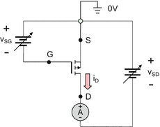

2.3 18.3 MOSFET Switching and Bias Circuits
18.3.1 Triode Region for Switching Circuits. Device Parameter Extraction
18.3.2 Resistor-Switch Model in Triode Region
Problem 18.32
A power MOSFET has the lumped process parameter \( {k}_n=130\kern0.5em \mathrm{m}\mathrm{A}/{\mathrm{V}}^2 \) and the threshold voltage of 2.0 V.
-
A.
Plot the drain current for drain-source voltages from the interval \( {\upsilon}_{\mathrm{DS}}=\left[0 \hbox{--} 9\right]\kern0.5em \mathrm{V} \) to scale and determine MOSFET turn-on resistance r DS given the gate-source voltage of 5 V.
-
B.
Plot the boundary between the triode region and the saturation region and indicate the slope 1/r DS in the figure.
-
C.
Plot r DS as a function of υ GS to scale.


Problem 18.33
Repeat the previous problem when the threshold voltage changes to 3 V.
Problem 18.34
A measurement curve for a certain NMOS transistor is shown in the figure below. Approximately determine the threshold voltage V Th and the (MOSFET) lumped process parameter k n (show units).

Problem 18.35
Repeat the previous problem for the measurement curve shown in the figure that follows.

Problem 18.36
The datasheet for an IRF510 enhanced-mode n-channel power MOSFET from Fairchild reports the average drain-source on-state resistance \( {r}_{\mathrm{D}\mathrm{S}}={\upsilon}_{\mathrm{D}\mathrm{S}}/{i}_{\mathrm{D}}=0.4\kern0.5em \Omega \) for \( {i}_{\mathrm{D}}=3.4\;\mathrm{A} \) and \( {\upsilon}_{\mathrm{GS}}=10\;\mathrm{V} \). Assuming threshold voltage to be 2.0 V, sketch r DS as a function of υ GS to scale.

18.3.3 Application Example: Output Resistance of Digital Logic Gates
Problem 18.37
For a logic gate shown in the figure that follows, construct the truth table in the form of Table 18.7 and determine the output gate resistance for every input voltage combination. Assume \( {V}_{\mathrm{DD}}>{V}_{\mathrm{Th}} \) for the NMOS transistor and \( {V}_{\mathrm{DD}}>\left|{V}_{\mathrm{Th}}\right| \) for the PMOS transistor. Label turn-on resistances of M 1,2,3,4 as r DS1,2,3,4.

Problem 18.38
For a logic gate shown in the figure that follows, construct the truth table in the form of Table 18.7 and determine the output gate resistance for every input voltage combination. Assume \( {V}_{\mathrm{DD}}>{V}_{\mathrm{Th}} \) for the NMOS transistor and \( {V}_{\mathrm{DD}}>\left|{V}_{\mathrm{Th}}\right| \) for the PMOS transistor. Label turn-on resistances of M 1,2,3,4,5,6 as r DS1,2,3,4,5,6.

18.3.4 MOSFET Circuit Analysis at DC
18.3.5 Application Example: Basic MOSFET Actuator
Problem 18.39
In a fixed-gate NMOS transistor circuit, the NMOS transistor has the lumped process parameter \( {k}_n=1.0\kern0.5em \mathrm{m}\mathrm{A}/{\mathrm{V}}^2 \) and the threshold voltage of 1.0 V. Furthermore, \( {V}_{\mathrm{GS}}=7\kern0.5em \mathrm{V} \), \( {V}_{\mathrm{DD}}=10\kern0.5em \mathrm{V} \), and \( {R}_{\mathrm{D}}=1\kern0.5em \mathrm{k}\Omega \). The corresponding υ DS – i D curve is shown in the figure that follows.
-
A.
Draw the load line in the same figure and find the solution for the drain-source voltage υ DS and drain current i D.
-
B.
Solve the same problem exactly and compare the two answers.


Problem 18.40
In a fixed-gate NMOS transistor circuit shown in the figure that follows, the NMOS transistor has the lumped process parameter \( {k}_n=1.0\kern0.5em \mathrm{m}\mathrm{A}/{\mathrm{V}}^2 \) and the threshold voltage of 1.0 V. Furthermore, \( {V}_{\mathrm{DD}}=15\kern0.5em \mathrm{V} \), and \( {R}_{\mathrm{D}}=1\kern0.5em \mathrm{k}\Omega \). Determine the region of operation of the transistor and find the solution for the drain-source voltage υ DS and drain current i D when
-
A.
\( {V}_{\mathrm{GS}}=1\kern0.5em \mathrm{V}. \)
-
B.
\( {V}_{\mathrm{GS}}=3\kern0.5em \mathrm{V}. \)
-
C.
\( {V}_{\mathrm{GS}}=5\kern0.5em \mathrm{V}. \)
-
D.
\( {V}_{\mathrm{GS}}=7\kern0.5em \mathrm{V}. \)

Problem 18.41
A solution for an unknown fixed-gate circuit shown in the previous problem is given in the figure that follows. Restore the transistor and circuit parameters (show units):
-
A.
\( {V}_{\mathrm{DD}} \)
-
B.
\( {V}_{\mathrm{GS}}-{V}_{\mathrm{Th}} \)
-
C.
\( {R}_{\mathrm{D}} \)
-
D.
\( {k}_n \)

Problem 18.42
In the circuit shown in the figure that follows, the NMOS transistor has the lumped process parameter k n and the threshold voltage V Th. Derive the analytical expression for the drain current i D as a function of V DD valid for any values of V DD.

Problem 18.43
In the circuit shown in the figure that follows, the PMOS transistor has the lumped process parameter k p and the threshold voltage \( {V}_{\mathrm{Th}}<0 \). Derive the analytical expression for the drain current i D as a function of V DD valid for any values of V DD.

Problem 18.44
In the circuit shown in the figure that follows, the NMOS transistor has the lumped process parameter k n and the threshold voltage V Th. Derive an analytical expression for the drain current i D as a function of V DD and R D valid for any values of V DD, R D.

Problem 18.45
In the circuit shown in the figure to the previous problem, a sufficiently large resistance R D has been chosen so that the drain current is very small. Measured υ DS is 2.5 V. What is approximately the threshold voltage V Th of the transistor?
Problem 18.46
In a fixed-gate NMOS transistor circuit shown in the figure, the NMOS transistor has the lumped process parameter \( {k}_n=100\kern0.5em \mathrm{m}\mathrm{A}/{\mathrm{V}}^2 \) and the threshold voltage of 2.0 V. Furthermore, \( {V}_{\mathrm{DD}}=20\kern0.5em \mathrm{V} \), \( {R}_2=1\kern0.5em \mathrm{k}\Omega \), and \( {R}_{\mathrm{D}}=40\kern0.5em \mathrm{k}\Omega \). Determine υ GS, the region of operation of the transistor, and the solution for the drain-source voltage υ DS and drain current i D when
-
A.
\( {R}_1=9\kern0.5em \mathrm{k}\Omega . \)
-
B.
\( {R}_1=4\kern0.5em \mathrm{k}\Omega . \)
-
C.
\( {R}_1=2.33\kern0.5em \mathrm{k}\Omega . \)
-
D.
\( {R}_1=1.5\kern0.5em \mathrm{k}\Omega . \)
At which value of the resistance R 1 is the load power (power into R D) maximized?
At which value of the resistance R 1 is the MOSFET power loss minimized?

Problem 18.47
Repeat the previous problem when the lumped process parameter changes to 200 mA/V2 .
2.4 18.4 MOSFET Amplifier
18.4.1 MOSFET Common-Source Amplifier
18.4.2 Voltage Transfer Characteristic
18.4.3 Principle of Operation and Q-point
18.4.4 MOSFET Biasing for Amplifier Operation
Problem 18.48
In the common-source amplifier circuit in Fig. 18.27, the MOSFET has the lumped process parameter \( {k}_n=100\kern0.5em \mathrm{m}\mathrm{A}/{\mathrm{V}}^2 \) and the threshold voltage of 2 V. The source voltage is \( {V}_{\mathrm{DD}}=20\kern0.5em \mathrm{V} \).
-
A.
Identify all values of υ IN corresponding to the saturation region when
$$ {R}_{\mathrm{D}}=1\kern0.5em \mathrm{k}\Omega . $$$$ {R}_{\mathrm{D}}=500\kern0.5em \Omega . $$$$ {R}_{\mathrm{D}}=100\kern0.5em \Omega . $$ -
B.
Identify the DC Q-point voltage V IN within the saturation region corresponding to \( {V}_{\mathrm{OUT}}={V}_{\mathrm{DD}}/2 \) when
$$ {R}_{\mathrm{D}}=1\kern0.5em \mathrm{k}\Omega . $$$$ {R}_{\mathrm{D}}=500\kern0.5em \Omega . $$$$ {R}_{\mathrm{D}}=100\kern0.5em \Omega . $$
Problem 18.49
Plot to scale the voltage transfer characteristic for the common-source amplifier circuit in Fig. 18.27 built with the general-purpose 2 N7000 NMOS transistor from Fairchild, which has the lumped process parameter \( {k}_n=90\kern0.5em \mathrm{m}\mathrm{A}/{\mathrm{V}}^2 \) and the threshold voltage of 2.0 V. Indicate the saturation region. The source voltage is \( {V}_{\mathrm{DD}}=10\kern0.5em \mathrm{V} \) and \( {R}_{\mathrm{D}}=90\kern0.5em \Omega \). Assume that the output voltage is constant in the triode region for simplicity.

18.4.5 Small-Signal MOSFET Model and Superposition
18.4.6 MOSFET Transconductance
18.4.7 Analysis of Common-Source MOSFET Amplifier
Problem 18.50
In a common-source MOSFET amplifier in Fig. 18.30a, the transistor has \( {k}_n=100\kern0.5em \mathrm{m}\mathrm{A}/{\mathrm{V}}^2 \) and \( {V}_{\mathrm{Th}}=3\kern0.5em \mathrm{V} \). Furthermore, \( {V}_{\mathrm{DD}}=20\kern0.5em \mathrm{V} \). For
-
A.
\( {R}_{\mathrm{D}}=5\kern0.5em \mathrm{k}\Omega \)
-
B.
\( {R}_{\mathrm{D}}=1\kern0.5em \mathrm{k}\Omega \)
-
C.
\( {R}_{\mathrm{D}}=100\kern0.5em \Omega \)
design the amplifier by performing the following steps:
-
1.
Identify all values of V GS corresponding to the Q-point in the saturation region.
-
2.
Determine V GS which assures that the Q-point (the DC operating point) is in saturation region and there is enough dynamic range for the output voltage to swing in both a positive and negative direction, i.e., \( {V}_{\mathrm{DS}}={V}_{\mathrm{DD}}/2 \).
-
3.
Determine the transistor’s transconductance at the Q-point.
-
4.
Determine the open-circuit small-signal voltage gain A υ0 of the amplifier.
Problem 18.51
-
A.
Repeat the previous problem when \( {R}_{\mathrm{D}}=120\kern0.5em \Omega \).
-
B.
Plot input and output voltages \( {\upsilon}_{\mathrm{IN}}(t)={V}_{\mathrm{GS}}+{\upsilon}_{\mathrm{in}}(t) \), \( {\upsilon}_{\mathrm{OUT}}(t)={V}_{\mathrm{DS}}+{\upsilon}_{\mathrm{out}}(t) \) to scale over two periods given that \( {\upsilon}_{in}(t)=0.1\kern0.5em \cos \left(\omega \kern0.1em t\right)\kern0.5em \left[\mathrm{V}\right] \).
Problem 18.52
-
A.
Repeat Problem 18.50 when \( {R}_{\mathrm{D}}=120\kern0.5em \Omega \) and \( {V}_{\mathrm{DD}}=10\kern0.5em \mathrm{V} \).
-
B.
Plot input and output voltages \( {\upsilon}_{\mathrm{IN}}(t)={V}_{\mathrm{GS}}+{\upsilon}_{\mathrm{in}}(t) \), \( {\upsilon}_{\mathrm{OUT}}(t)={V}_{\mathrm{DS}}+{\upsilon}_{\mathrm{out}}(t) \) to scale over two periods given that \( {\upsilon}_{\mathrm{in}}(t)=0.2\kern0.5em \cos \left(\omega \kern0.1em t\right)\kern0.5em \left[\mathrm{V}\right] \).
Rights and permissions
Copyright information
© 2016 Springer International Publishing Switzerland
About this chapter
Cite this chapter
N. Makarov, S., Ludwig, R., Bitar, S.J. (2016). MOS Field-Effect Transistor (MOSFET). In: Practical Electrical Engineering. Springer, Cham. https://doi.org/10.1007/978-3-319-21173-2_18
Download citation
DOI: https://doi.org/10.1007/978-3-319-21173-2_18
Publisher Name: Springer, Cham
Print ISBN: 978-3-319-21172-5
Online ISBN: 978-3-319-21173-2
eBook Packages: EngineeringEngineering (R0)