
Abstract
Among the shape-memory alloys (SMAs), nitinol (Ni–Ti alloys) is the most vital because of its very good wear and corrosion properties along with excellent mechanical properties. Nitinol has gained significant interest as micro/nano-electromechanical system (M/NEMS)-based micro/nano-actuators which are precision control devices that work based on mechanical forces at the microscale level. Other advantages of nitinol including large actuation force, high ratio of power to weight, large deformation, and high frequency response lead to a faster response in the micron-size actuators. The magnetron sputtering technique is the most effective technique to make nitinol with the desired composition for shape-memory application. The phase transformation and shape-memory behavior of nitinol-based microactuators are very sensitive to mechanical factors and sputtering-related variable parameters. Several works were carried out to fabricate nitinol with the desired composition using magnetron co-sputtering of Ti elemental target and Ni–Ti alloy target. In addition to that, nitinol was also developed using magnetron co-sputtering of individual Ni and Ti elemental targets by regulating their target power. Magnetron co-sputtering method was found incredibly simple and flexible to monitor the composition of the nitinol. In this book chapter, the dependency of the transformation and shape-memory behavior of nitinol on composition, annealing temperature, sputtering pressure, sputtering power, and growth temperature has been explained for both Ni-rich and Ti–rich Ni–Ti shape-memory alloys. Further, the application of nitinol in micromachines such as micromanipulators and fluid microvalves has been discussed.
Access provided by Autonomous University of Puebla. Download chapter PDF
Keywords
3.1 General Background
In the recent past, nitinol-based thin-film alloys have played an important role in modern technology because of their functional properties. In order to use the nitinols in the fabrication of Micro-Electromechanical Systems (MEMSs), it is required to fabricate Ni–Ti alloy films of thickness below micron size. This condition can be easily achieved by using the magnetron sputter deposition technique [1]. Nitinol-based alloy films developed using the magnetron sputter technique are considered to be applied in the fabrication of micro-electromechanical devices. In addition, equiatomic Ni–Ti alloy is the most desirable for study to use in MEMS due to numerous reasons: its large resistance to deformations, large recovery strain, high recovery stress, biocompatibility, a high ratio of power to weight, decent mechanical property, excellent fatigue resistance, quite low driving voltage, and easy design. It has also been reported that Ni–Ti alloy film has the highest work density which is useful for the shape-memory effects [2]. However, the response time is not so fast in comparison to others, and this problem can be overcome by reducing the thickness below submicron size which allows small heat flow involved during cooling and heating. For these reasons, the demand for fabricating powerful micro-actuators which drive the MEMS device using the Ni–Ti thin films has been ever-increasing [2,3,4,5,6]. The Ni–Ti alloys can reversibly transform to its low-temperature crystallographic structure from its high-temperature crystallographic structure, that is to the monoclinic phase (B19, martensite) from the CsCl (B2, austenite), directly or through the intermediate rhombohedral phase (R-phase). And because of this austenite to martensitic transition, the Ni–Ti alloy films exhibit shape-memory behavior [7, 8]. To utilize the properties exhibited by shape-memory alloys, some factors need to be considered, for example, regulating Ni–Ti alloys composition and their heat treatment which helps in fabrication and processing. The most important feature of the martensitic transition is the start and finish temperatures which have been observed to be dependent on the processing techniques and composition of the Ni–Ti alloy films [9]. The working temperature of the micro-electromechanical devices is controlled by the composition of the Ni–Ti alloy films, since temperatures required for the phase transformation are sensitive to the ratio of Ti and Ni in the Ni–Ti alloy films. The variation in 1% of composition can result in a shift in transformation temperature of about 100 °C. In addition to governing the composition of Ni–Ti alloy films, other relevant parameters such as contamination of the Ni–Ti alloy films during processing due to the formation of oxides of titanium and compatibility with conventional designing processes of microdevices must be considered [10,11,12].
Additionally, the thin-film applications in the micro/nano-electromechanical systems (M/NEMS) have driven extensive research toward the processing-microstructure and characterization of Ni–Ti alloy thin films using different techniques. Though a number of techniques have been applied for the fabrication of Ni–Ti alloy films such as cathodic arc plasma ion plating, flash evaporation, sputtering, and laser ablation, in actual practice, the sputter deposition technique has got huge success in achieving the desired composition and microstructural properties [13, 14]. In sputtering, when the alloy target of Ni–Ti is used, then Ni-rich Ni–Ti alloy films have been formed in comparison to the sputtering of the individual targets due to the higher sputtering yield for Ni than Ti at the same power [14]. This problem can be avoided by placing pure Ti onto the target in the form of small pieces [15]. Otherwise, near-equiatomic Ni–Ti alloy films can be obtained using magnetron co-sputtering of a pure Ti target along with the Ti-enriched Ni–Ti alloy target or changing the sputter gas pressure inside the chamber [16, 17]. However, by varying the sputter gas pressure, it is difficult to regulate the composition of Ni–Ti alloy films because high gas pressures lead to poor microstructure and brittleness [18]. So, by regulating the individual target power ratio of Ti and Ni during magnetron co-sputtering, the Ni–Ti alloy film composition can be controlled. The most important advantage of the magnetron co-sputtering technique over other techniques is that its ability to produce alloy films with the desired composition using appropriate element target power [10, 19].
3.2 Ni–Ti Alloys’ Phase Diagram
The Ni–Ti alloys’ phase diagram had been provocative till the 1980s. The Ni–Ti alloys reveal numerous precipitates during their heat-treatment processes and there was no such phase diagram that helps to understand this process until the 1980s. Further, Massalski et al. [20] had proposed the phase diagram of Ni–Ti system which was able to explain this system quite well. The representative Ni–Ti alloy phase diagram is shown in Fig. 3.1.

Reprinted from [7]. Copyright (1999) with permission from Elsevier Science S.A.
Shows the Ni–Ti alloys’ phase diagram.
The importance of the Ni–Ti alloys phase diagram is because of their various heat-treatment processes and enhancement in their shape-memory properties. Laves and Wallbaum were the first to recognize the single-phase Ni–Ti alloy near the equiatomic composition at higher temperatures. The single-phase Ni–Ti has an ordered structure [B2 (CsCl) type] at room temperature which plays a crucial role in the martensitic phase transformation which is responsible for the shape-memory behavior in the Ni–Ti alloy system. On the Ti–rich side, Ti2Ni phase is formed which is cubic. On the Ni-rich side, TiNi3 phase is formed. On the nickel-rich side, the formation of Ti3Ni4, Ti2Ni3, and TiNi3 has been reported, and over a period, there was confusion about whether a eutectoid reaction is occurring. The order–disorder transition temperature is at 1090 °C. The variation in atomic percentage should be kept close to the equiatomic composition for the excellent shape-memory properties since precipitates do not contribute to shape-memory behavior [21].
3.3 The Shape-Memory Effect in Nitinol (Ni–Ti Alloys)
Nitinol is one of the most significant shape-memory alloys [SMAs] having very good mechanical properties, excellent wear, and corrosion properties. The reasons for the shape-memory behavior in nitinol include not only martensitic phase transformation (which is diffusion less transformation) causes for shape-memory and pseudoelastic effects, but also diffusion transformations to improve shape-memory characteristics.
3.4 Ni–Ti Alloys Processed by Magnetron Sputtering
In many studies, it had been shown that the Ni–Ti film processed by magnetron co-sputter deposition was amorphous. The formation of amorphous film during the sputtering process might be due to the non-equilibrium conditions [22]. If there are more than three different kinds of elements with atomic size ratios above 12% and have the heat of mixing negative, then the glass will be formed by the constituent elements. This empirical rule for metals’ ability to form glass was proposed by Inoue [23]. For the Ni–Ti alloy system, there are only two elements, Ni and Ti in place of three, but then again, the difference in atomic size is 19% (Ni atomic radius = 0.124 nm and Ti atomic radius = 0.147 nm), and the standard value of enthalpy of formation is −33.1 kJ/mol atom. Therefore, these reasons are proper to understand the amorphous nature of Ni–Ti alloy. Another explanation for the formation of amorphous Ni–Ti alloy film formed by sputter deposition technique given by Chu et al. [22] is that the higher temperature for the sputtered Ni–Ti atoms as compared to the substrate on which these atoms get deposited. Therefore, the substrate is at a lower temperature and behaves as a heat sink for the magnetron co-sputter-deposited Ni–Ti alloy atoms [24]. The lodging time required for the adatom to be in equilibrating with the depositing substrate has been predicted of the order of 10–12 s. The equivalent temperature for the adatom having energy 0.1 eV is equal to 1000 °C, and during deposition, the atoms are acquired at approximately 1015 °C/s of quenching rate [25]. The quenching rates for the sputter-deposited atoms are very much faster and have significantly high energy. Previous studies had shown the non-equilibrium atomic arrangements at high quenching rates which leads to amorphous microstructures in the developed films [26].
Ni–Ti alloys may be broadly categorized into equiatomic and near-equiatomic alloys (Ti–rich and Ni-rich alloys). For the bulk Ni–Ti alloy systems, on the Ni-rich side, the shape-memory properties can be improved by the Ti3Ni4 precipitates unless Ni content reaches nearly 50%. On the other hand, on the Ti–rich side, Ti2Ni precipitates show poor shape-memory characteristics, because on the Ti–rich side, the solubility limit is almost vertical. However, for the crystallized Ni–Ti alloy films, this situation changes through a non-equilibrium amorphous state. At substrate temperature lower than 473 K, the as-deposited Ni–Ti films are amorphous in nature. Crystallization temperature depends upon the composition of the Ni–Ti films. For the compositions Ti–51.1Ni and Ti–50.4Ni, crystallization temperature was observed at 756 K [21]. The heat-treatment temperature decides the grain size of crystallized Ni–Ti alloy films. The reported grain size ranges from 1 μm to 4 μm, which is significantly smaller than the grain size for bulk Ni–Ti alloys [21].
3.5 Ni-Rich Ni–Ti Thin Films
From the extensive researches in the past, it has already been established that magnetron co-sputter-deposited Ni–Ti alloy thin films exhibit very good mechanical properties due to their extremely fine grain size. The composition of Ni–Ti alloy films decides the phase transformation behavior is a function of temperature, as shown in Fig. 3.2. It shows very similar phase transformation behavior as the bulk Ni–Ti alloys. For the near-equiatomic Ni–Ti alloy films, the transformation behavior shown in Fig. 3.2a displays a single-stage \({\text{B2}}\, \to \,\text{B19}^{\prime}\) phase transformation, while for Ni-rich Ni–Ti alloy films, the phase transformation behavior shown in Fig. 3.2b displays two-stage \({\text{B2}}\, \to \,{\text{R}}\, \to \,\text{B19}^{\prime}\) phase transformation, because Ti3Ni4 precipitates suppress \({\text{B2}}\, \to \,\text{B19}^{\prime}\) transformation relative to \({\text{B2}}\, \to \,{\text{R}}\) transformation alike bulk Ni–Ti alloys [27].

Reprinted with permission from Springer Nature: The Materials Research Society Online Proceedings Library [28]. Copyright © 2021
Shows at constant stresses, the strain versus temperature curves of Ni–Ti alloy films: a Near-equiatomic Ni–Ti and b Ni-rich Ni–Ti alloys heat treated at 773, 873, and 973 K for 1 h. Further, Fig. 3.2a shows one-stage phase transformation for all the temperature, and (b) shows two-stage phase transformation at 773 K; on the other hand, it shows one-stage phase transformation for temperatures 873 and 973 K.
In more detail, the transformation behavior, which is a function of composition as well as the condition of heat treatment, is shown in Fig. 3.3. The phase transformation behavior, microstructures, and mechanical properties for Ni-rich Ti–Ni alloy thin films are the same as the bulk Ni–Ti alloys. In this alloy, the superelasticity, one-way shape-memory effect, and two-way shape-memory effect have been observed. All these properties of this alloy have been discussed in detail in the review paper by Otsuka et al. [21].

Reprinted from [8]. Copyright © (1999) with permission from Elsevier Science S.A.
Shows the variation in phase transformation behavior for Ni-rich and near-equiatomic Ni–Ti alloy thin films because of the variation in heat-treatment temperature.
3.6 Ti–rich Ti–Ni Thin Films
For the Ti–rich side of the Ni–Ti alloy, Ti2Ni precipitates appear only at grain boundaries because of the almost vertical solubility limit, as shown in Fig. 3.1. Therefore, in these alloy films, it is almost impossible to improve shape-memory properties by using precipitation. However, in such a case if alloys have been prepared through an amorphous state, then there is a possibility for uniform precipitation because amorphous Ni–Ti alloy film can supersaturate Ti atoms, and thereafter, excess Ti atoms may get precipitated upon crystallization. A detailed investigation on Ti–rich Ti–Ni alloy films is given below.
Nakata et al. [29], in 1995, observed a thin plate of Ti2Ni precipitates surrounded by heavy strain contrast for the Ti–rich Ni–Ti alloys which is similar to GP-zones in Al–Cu alloy, obtained during heat treatment of the Ti51.5Ni48.5 alloy films for 600 s at 773 K. Similar results were observed by Zhang et al. [30] for the Ni–Ti alloy, as shown in Fig. 3.4. It was similar to GP-zones with a few atomic layers or monolayers in the B2 matrix.

Reprinted from [31]. Copyright © (2001) with permission from Acta Materialia Inc. Published by Elsevier Ltd.
High magnification images of GP-zones in the Ni–Ti alloy a annealed at 773 K for 30 min and b annealed at 823 K for 1 h. The inset representscorresponding diffraction pattern.
In 1996, Kajiwara et al. [31] reported that for the heat-treated Ti51.8Ni48.2 alloy film at 745 K, which is almost equal to crystallization temperature, similar thin plate precipitates appeared. The examination of these precipitates under high-resolution electron microscopy (HRTEM) revealed that the B2 matrix and Ti2Ni precipitate lattice are continuous, which suggests the coherency of the precipitate. From the diffraction pattern, there has been also deduced body-centered tetragonal (BCT) structure of the precipitate due to the precipitation of excess Ti in Ni–Ti alloys on {100} B2 plane. Another work [30, 32] observed a similar structure for the precipitates by examining the bright contrast of the precipitate, as revealed in Fig. 3.5, because precipitates appear bright as compared to the matrix elements. There were also carried out simulations for the imaging of these thin precipitated plates built on the model of the the layers precipitates of excess Ti in Ni–Ti alloys on {100} B2 planes. Though, instead of bright contrast, only dark contrast was observed using this model. Only after the introduction of vacancies in addition to Ti atoms, bright contrast was obtained. Therefore, it was considered that about 20% Ti atoms in the thin plate of precipitates were substituted by vacancies. This is the vital difference between these two studies on the structure of precipitates. Since the distribution of precipitates is homogeneous, Kajiwara et al. [33] considered that Ti2Ni precipitates appear only after the crystallization.

Reprinted from [30]. Copyright © (2001) with permission from Acta Materialia Inc. Published by Elsevier Ltd.
Shows high-resolution TEM image of GP-zones for Ni–Ti alloy annealed at 773 K for 5 min (observed in martensite state).
In this mechanism, it is presumed that the excess Ti atoms are somehow held within the matrix even after crystallization. Kajiwara et al. [33] also observed another morphology of the thin plate precipitate after the heat treatment of Ni–Ti alloy films at a lower temperature of about 50 K than the crystallization temperature. In this situation, most of the particles in the size range of 0.1–1 μm are associated with the crystallized films, and each particle consists of several nanocrystals of sizes varying from 20 to 40 nm. These nanocrystals are surrounded by the thin plate precipitates grown on {100} B2 planes and have the same orientation in each particle. The following mechanism is considered for the formation of this microstructure. First, a nanocrystalline B2 structure is formed upon crystallization. Then excess Ti atoms present in the B2 matrix are pushed out in the amorphous region surrounding the nanocrystals and producing thin plates of precipitates on {100} B2 planes. The above morphology is created on replication of this process. There has been also examined the mechanical properties of thin films of nitinol. It has been reported that the Ni–Ti alloy films with thin plate precipitates show great shape-memory behavior, as shown in Fig. 3.6. This also shows that without introducing plastic strain, there is a 5.5% recovery in the strain at 240 MPa stress. Likewise, Fig. 3.7a reveals that with decreasing heat-treatment temperature, the critical stress necessary for a slip in amorphous Ni–Ti alloy films increases rapidly, and it levels off at temperatures above 820 K. At this temperature (820 K), thin plate precipitates change to granular Ti2Ni particles.

Reprinted with permission from [31]. Copyright © 1996 Taylor & Francis Ltd.
Shows strain versus temperature plots for the heat-treated 51.8Ti–48.2Ni alloy film, at 745 K for one hour using constant stresses.

Reprinted with permission from [31]. Copyright © 1996 Taylor & Francis Ltd.
a Shows the critical stress required for slip versus heat-treatment temperature plot, and b shows the recoverable strain versus heat-treatment temperature plot for the 51.8Ti–48.2Ni alloy thin films.
Figure 3.7b confirms that the recovery in strain is a function of heat-treatment temperature. This shows that at lower heat-treatment temperatures, the recovery in strain is larger. The increase of recovery in strain above 750 K is due to the high diffusion rate at a higher temperature. This means for the improvement in mechanical properties, the thin plate precipitates are more important.
In 1995, studies on the crystallization behavior of Ni–Ti shape-memory alloy started [29, 34], and in the B2 matrix, granular Ti2Ni precipitates were observed above the critical temperature. In this condition, there were two classes of orientation relationships concerning the B2 matrix.
When excess Ti atoms percentage was lesser than about 53%, then granular Ti2Ni precipitates had a definite orientation relationship with the B2 matrix. Ishida et al. [35] were the first to determine the orientation relationship as
 ; that is, the crystal axes of Ti2Ni precipitates and the B2 matrix are parallel to each other. However, when excess Ti atoms percentage was more than 53%, then granular Ti2Ni precipitates were formed first, and then crystallization happened. Therefore, B2 matrix and granular Ti2Ni precipitates had no specific orientation relationship. In detail, the relation between heat-treating condition, composition, and microstructures is shown in Figs. 3.8 and 3.9 which was first made by Kawamura et al. [36] and later modified by Ishida [9].

Reprinted with permission from Springer Nature: The Materials Research Society: MRS Bulletin [9]. Copyright © 2002
a Solid squares
 represent granular Ti2Ni precipitates having a random orientation concerning B2 matrix; b open squares
 represent granular Ti2Ni precipitates having the same orientation concerning B2 matrix; c open triangles
 represent thin plate precipitates and Ti2Ni precipitates; d solid circles
 represent thin plate precipitates grown at higher temperature and e thin plate precipitates grown at a lower temperature; f open circles
 represent no precipitates; and solid triangles
 represent amorphous Ni–Ti film and, for Ti–rich Ni–Ti alloy, thin films heat treated at different temperatures for 1 h. The above-mentioned alphabets a–f also belong to the text figure of Fig. 3.9.

Reprinted with permission from Springer Nature: The Materials Research Society: MRS Bulletin [9]. Copyright © 2002
Shows bright-field TEM micrographs of Ni–Ti alloys with various compositions and heat treatment and the corresponding electron diffraction patterns shown as insets. The alphabets a–f correspond to those in the previous Fig. 3.8.
In Fig. 3.8, where Ti atoms percentage was lower than 53%, granular morphology of Ti2Ni is developed in place of thin plate morphology along with the increase in heat-treatment temperature, but then again there is a region where granular morphology and thin plate morphology coexist (indicated by a symbol Δ) in between.
The network alike patterns along < 110 > directions were observed for the Ni–Ti alloys by Otsuka et al. [21], as shown in Fig. 3.9b, c. These images are of B2 matrix and granular Ti2Ni. They also noticed that there were two different morphologies in the G.P. zone region, as shown in Fig. 3.9d, e. These images represent the morphologies that are related to thin plate precipitates heat treated at a temperature closer to crystallization temperature and lower than crystallization temperature, respectively. Near equiatomic Ni–Ti alloy films, there were no precipitates. Moreover, Ti–rich Ti–Ni alloy thin films show superelasticity [37], two-stage phase transformation via R-phase as well as two-way shape-memory effect [38], as shown in Fig. 3.6. In these alloy films, the phase transformation temperatures are greater than the Ni-rich Ni–Ti alloy films, because the martensitic transformation temperature of Ni–Ti alloy films has a propensity to decrease with increasing Ni content in Ni-rich Ni–Ti alloy, whereas it is almost constant for the Ti–rich Ni–Ti alloy [39].
Besides the Ni–Ti binary alloy, the examination of ternary shape-memory alloy is also interesting. Among these, Ni–Ti–Cu, Ni–Ti–Pd, and Ni–Ti–Hf ternary alloy are the most promising for the shape-memory behaviors [40]. The Ni–Ti–Cu ternary alloy thin films are quite fascinating for the design of actuators with small temperature hysteresis. However, Ni–Ti–Pd and Ni–Ti–Hf ternary alloy thin films are promising for the high-temperature shape-memory behavior.
3.7 Influence of Various Processing Parameters Related to Magnetron Sputtering on Film Quality
Relevant parameters which affect the microstructure and properties of the Ni–Ti alloy thin films are as follows:
-
(1)
Target power.
-
(2)
Substrate–target distance.
-
(3)
Substrate temperature.
-
(4)
Substrate rotation.
-
(5)
Substrate bias.
-
(6)
Ar gas pressure.
-
(7)
Deposition geometry.
-
(1)
Target Power: As the target power increases, a greater number of atoms will be ejected because Ar ions will strike the target with more energy thus increasing the deposition rate [41]. The sputtering rate is known to scale with the applied target power [42, 43]. It has been shown that the sputtering rate is related to the target power through the following relation [44]:
$$\left( {{{{\text{dN}}} \mathord{\left/ {\vphantom {{{\text{dN}}} {{\text{dt}}}}} \right. \kern-\nulldelimiterspace} {{\text{dt}}}}} \right) = {{{\text{AYI}}} \mathord{\left/ {\vphantom {{{\text{AYI}}} {\text{e}}}} \right. \kern-\nulldelimiterspace} {\text{e}}}$$(3.1)where N is the number of sputtered atoms, A is the area of the target, Y is the sputtering yield, I is the ion current, and e is the electronic charge. If the power is kept constant, then if there is an increase in the sputtering gas pressure, there is an increase in ion density. For low target power, the use of high pressure leads to lowering of the kinetic energy of the sputtered atoms because of the increased number of inelastic collisions with sputtering gas ions.
-
(2)
Substrate–Target Distance: Substrate–Target distance (STD) is a crucial parameter influencing the deposition rate, and this has been well investigated by Wuhrer et al. [45]. If the value of STD is increased, the sputtered atoms have to travel more before reaching the substrate. During their travel, the atoms are easily scattered by collision with gas ions in the chamber, and therefore, the mean free path becomes shorter. As a result, only fewer atoms can reach the substrate. The deposition rate (R) is related to the prominent sputtering parameters by the following relation [46]:
$${\text{R}} = {{{\text{k}} \cdot {\text{P}}} \mathord{\left/ {\vphantom {{{\text{k}} \cdot {\text{P}}} {\rho \cdot \left( {{\text{STD}}} \right)}}} \right. \kern-\nulldelimiterspace} {\rho \cdot \left( {{\text{STD}}} \right)}}$$(3.2)where P is the target power, ρ is gas pressure, and k is the proportionality constant which depends on the target materials and the type of the gas used for sputtering.
-
(3)
Substrate Temperature: From the phase diagram of the Ni–Ti alloys, it is clear that the Ni–Ti alloy is stable above the temperature Te ≈ 630 °C. Therefore, the Ni–Ti alloy thin films deposited at room temperature are unstructured but after the post-annealing above Te, the films’ nature becomes crystalline. The crystalline Ni–Ti alloy films can also be grown by using in situ heating of the substrates at a relatively higher temperature. It has been observed that the 300–450 °C substrate temperature is sufficient to get crystalline Ni–Ti alloy films with fantastic shape–memory properties [10, 47].
-
(4)
Substrate Rotation: Krulevitch et al. [11] observed that the magnetron sputtering technique for the deposition of Ni–Ti–Cu alloy films from Cu, Ti, and Ni targets with zero substrate rotation speed leads to a significant change in composition. In the absence of substrate rotation, the composition variation across the Ni–Ti-deposited substrate, where the target power of Ti was around three times more than the target power of Ni to maintain the same deposition rate of Ti and Ni, is shown in Fig. 3.10a. However, compositional uniformity was easily obtained for the Ni–Ti alloy films using substrate rotation. The variation in composition for the Ti–rich Ni–Ti films, near-equiatomic Ni–Ti films, and Ni-rich Ni–Ti films is shown in Fig. 3.10b [12].
Fig. 3.10 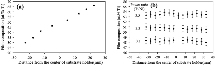
Reprinted from [12] Copyright © (2005) with permission from Elsevier B.V.
Shows the variation in composition across the substrate a without substrate rotation and b with substrate rotation for the three different ratios of target power.
-
(5)
Substrate Bias: Substrate bias is the most effective parameter related to magnetron sputtering which was used for the formation of equiaxed grains in a microstructure whereas films formed without bias were mostly columnar as observed and nicely explained by R. Mitra et al. [48]. For the columnar microstructure, because of intercolumnar porosity, the density is expected to be lower, as shown in Fig. 3.11a, b, and hence in the transverse direction, the mechanical properties will be worse. Negative substrate bias increases the momentum of the sputter gas ions striking the growing films which break the columnar structure rising from the islands on the substrate by hitting the atoms into their nearest valleys. But at the same time, it leads to a higher rate of re-sputtering of atoms from the growing film which may cause a rough filmsurface.
Fig. 3.11 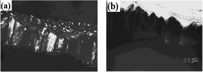
Reprinted with permission from Springer Nature: The Materials Research Society: Journal of Materials Research [48]. Copyright © 2001
Shows the TEM images of Ni film developed at room temperature in the absence of substrate bias: a dark-field image reveals equiaxed grains on the top and columnar grains below, and b bright-field image reveals the presence of columnar porosities as indicated by arrows.
-
(6)
Ar Gas Pressure: The Ar gas pressure generally controls the energies of the depositing atoms and therefore affects the microstructure, film density, and stress developed in the films. At low Ar gas pressures, the microstructure is denser with lesser defects, while at higher Ar gas pressures, the deposited films show microstructural defects and lower density. Sohrab et al. [12] observed that films having a range of compositions, grown at Ar gas pressures greater than one pascal (Pa), had cracks on the surface with brittle microstructure, as shown in Fig. 3.12a which reveals the wide delamination at the Ni–Ti/Si interface and cracks on the surface because of the tensile residual stress. Films prepared at low Ar gas pressures with the same composition showed a relatively smoother surface with featureless structure, as shown in Fig. 3.12b.
Fig. 3.12 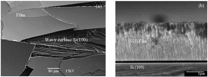
Reprinted from [12]. Copyright © (2005) with permission from Elsevier B.V.
a Shows SEM plan view micrograph of Ni–Ti/Si films deposited at 1.2 Pa Ar gas pressures, and b illustrates the FESEM cross-sectional micrograph of Ni–Ti/Si film developed at Ar gas pressure of 0.6 Pa.
Chu et al. [22] also reported the effect of Ar gas pressure on the microstructure of the sputter-deposited film. The films grown at Ar gas pressures higher than 7mTorr showed a well-defined cluster of columnar microstructures, as shown in Fig. 3.13a, b. However, the film prepared below 0.5 mTorr argon gas pressures reveals a dense microstructure, as shown in Fig. 3.13c. The columnar microstructures are responsible for the relatively larger grain size because of the inadequate mobility of the depositing atoms. The main reason for the columnar microstructures is the high argon gas pressure which leads to a decrease in the energy of atoms released from the target by sputtering leads to a decrease in adatoms mobility which eventually develops the columnar microstructure [49]. Moreover, at high gas pressures, argon atoms that are absorbed on the growing film surface could restrict the motion of depositing atoms which results in a columnar microstructure in the grown films [50]. Sohrab et al. [12] investigated Ni–Ti thin films deposited at high gas pressure for the shape-memory applications; despite controlling the composition, the Ni–Ti films showed poor shape-memory properties. Whereas the Ni–Ti films processed at relatively lower Ar gas pressures preferably showed better shape-memory effects. In addition to that, the films deposited at high gas pressures showed poor film microstructure which affects phase transformation behaviors. The annealing temperature also affects the shape-memory behavior of the Ni–Ti films.
Fig. 3.13 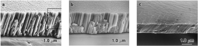
Reprinted from [22]. Copyright © (2000) with permission from Elsevier Science S.A.
Shows the cross-sectional SEM images of Ni–Ti alloy films processed at room temperature for constant time with Ar gas pressures of a 10 m Torr, b 7 m Torr, and c 0.5 m Torr.
-
(7)
Deposition Geometry: The appropriate deposition geometry also controls the composition uniformity. The substrate–target distance, size, and shape of targets and inclining the axes of the targets are included in deposition geometry [50].


3.8 Surface Topography of Sputter-Deposited Films
Surface topography plays an important role to impart a good functional characteristic to thin films. Extensive work on the surface topography of Ni thin films grown at room temperature and liquid nitrogen temperature by applying various substrate biasing conditions was carried out by Mitra et al. [48], as shown in Fig. 3.14a, b, c. It shows 2.0-μm-thick Ni films developed at room temperature at a negative substrate bias voltage of 0 V, −150 V, and −200 V, respectively. From Fig. 3.14, it is clear that the Ni film deposited at zero substrate bias voltage is having extra surface porosity as compared to the Ni films deposited at relatively higher negative substrate bias. The Ni films deposited by applying 0 V and 200 V substrate bias voltages reveal a rough surface morphology. The roughness and porosities in the Ni film deposited at 0 V substrate bias voltage, as shown in Fig. 3.14a, are mainly because of the columnar and tapered grains. Figure 3.11b reveals the intercolumnar or grain boundary voids with larger surface porosities. These grain boundary voids are generated during the time of nucleation of islands that are also prevented by intergrain shadowing effects which cause tapered crystallites with the columnar grain morphology. Therefore, the intergrain boundaries are not true grain boundaries because of the presense of voids.

Reprinted with permission from Springer Nature: The Materials Research Society: Journal of Materials Research [48]. Copyright © 2001
Shows optical micrographs of Ni films deposited at room temperature and 200 W target power with a negative substrate bias voltage of a 0 V, b −150 V, and c −200 V.
If the vacancies trapped in the grain boundaries have considerable mobility and coalesce, then the pores grow faster. The nanopores present at grain boundaries were also examined by TEM during the investigation of Ni films processed without a substrate bias voltage. By application of an intermediate substrate bias voltage, the entrapment of argon atoms is reduced because of the re-sputtering phenomenon that occurs due to argon ions bombardments. But at higher substrate bias argon entrapment is more, and a higher degree of re-sputtering causes a large concentration of points defects.
The surface morphology of Ni films grown at the temperature of liquid nitrogen has shown more surface porosity as compared to Ni films grown at room temperature. These things can be described by the inadequate mobility of the atoms on the growing film at a lower temperature. The sticking problem for the argon atoms reflected toward the growing film from the target materials would be more prominent while cooling the film growing substrate by liquid nitrogen as compared to room temperature. Whereas, during heating the substrate, the entrapped argon gas atom would escape from the surface and leave behind the pores.
The optical images of 2.0-mm-thick Ni films processed using negative substrate bias of 0 V and −150 V, at liquid nitrogen temperature, are shown in Fig. 3.15. From Fig. 3.15a, it is noticeable that Ni film surface deposited at 0 V substrate bias is very porous with larger pores size. On the other side, the Ni film surface deposited at −150 V substrate bias discloses fewer pores as compared to the Ni films deposited at 0 V substrate bias, as shown in Fig. 3.15b. It has been also examined that the Ni films grown at −150 V substrate bias (Fig. 3.15b) have a smoother surface relative to the Ni film deposited at 0 V substrate bias. Furthermore, the increase in negative substrate bias above −150 V leads to an increase in surface roughness of the deposited Ni film at room temperature as well as at liquid nitrogen temperature [48].

Reprinted with permission from Springer Nature: The Materials Research Society: Journal of Materials Research [48]. Copyright © 2001
Shows optical micrographs of the Ni films deposited at liquid nitrogen temperature using substrate bias voltage of a 0 V and b −150 V.
Moreover, it was reported that for the thick film deposited at −200 V substrate bias voltage, the surface roughness was quite high. The film surface roughness also increased with increasing film thickness due to the continued ion bombardment on the depositing surfaces [43].
3.9 Micro-Actuator
The micromachines such as micromanipulators and fluid microvalves with electronic behavior are pretty important and have important roles in different technologies and the design of various devices such as micromechanical devices, biotechnology, medicine industry, the semiconductor industry, precision optical devices, and automation technology. The nitinol (Ni–Ti alloys)-based Shape-Memory Alloy (SMA) films processed using sputter sputtering technique have potential applications in the making of micro/nano-electromechanical systems (M/NEMSs) and Bio-micro/nano-electromechanical systems-based microactuators (e.g., micro-positioners, microfluid pumps, microgrippers, and micro-wrapper), cantilevers, and stent for neurovascular blood vessels [18].
Nitinol-based shape-memory alloys are also considered as an essential material for generating actuation in M/NEMS-based devices, where periodic operation and large force/stroke have been required. This can be used in extreme environmental conditions, for example, biological, corrosive, and radioactive conditions. Therefore, the design of M/NEMS is a multi-disciplinary approach for their potential applications. Generally, the common microactuators, for example, microswitches and microsensors utilize shape-memory alloy (SMA) films for their inherent two-way shape-memory effect (TWSME) through a higher displacement, and homogenous composition among the film thickness. There may be variations in composition along with film thickness [51, 52]. The nitinol-based thin-film actuators can offer a quite large actuation force though foregoing their strain. With the help of suitable biasing force, the substrate of nitinol-based thin films can be activated and a mechanical TWSME with a relatively small actuation force is generated [53,54,55]. The two-way shape-memory effect (TWSME) can be realized in (1) entity of R-phase, (2) ability of aging and hot shaping, (3) their intrinsic residual stress, and (4) generation of the mechanical energy and displacement all through the phase transformation. The deformation in nitinol-based SMA actuators is generated because of the cooling and heating cycles which are the two most important parameters for the formation of SMA actuators [56, 57]. Nitinol-based SMA used in bimorph actuators provides a relatively much higher actuation force at a lower temperature which is essential to influence the fully actuated state that is austenitic phase as compared to other shape-memory alloy (SMA) materials [58]. The systematic design and development of nitinol-based micromanipulator developed using two bimorph micro-actuators together and its proposed application in handling small objects are shown in Figs. 3.16 and 3.17, respectively [59].

Reprinted from [59] Copyright © (2016) with permission from Elsevier Ltd.
Shows the advanced micromanipulator’s state: a off-state, b first link in actuated state, c both links in actuated state, d the gripper without actuation, and e the gripper with actuation.

Reprinted from [59] Copyright © (2016) with permission from Elsevier Ltd.
Shows the advanced micromanipulator application in handling small objects.
3.10 Conclusions
This book chapter comprises a study of nitinol-based shape-memory alloys with emphasis on the processing of these alloys by the physical vapor deposition technique. Based on the focus of the present work, the topic of magnetron sputtering has been dealt with in detail. The studies deal with the effect of magnetron sputter-related parameters on the structure and properties of Ni-rich and Ti–rich Ni–Ti alloys. This chapter indicates that the effect of process parameters on growth rate as well as structure and properties of the Ni–Ti alloys needs further study. Furthermore, an overview of the nitinol (Ni–Ti alloys)-based shape-memory alloys (SMAs) processed using the sputtering technique in the making of micro/nano-electromechanical systems has been presented.
References
Cho H, Kim HY, Miyazaki S (2005) Fabrication and characterization of Ti–Ni shape-memory thin film using Ti/Ni multilayer technique. Sci Technol Adv Mater 6:678–683
Hae-Yong NOH, Kwang-Koo JEE, Kyu-Hwan LEE, Young-Kook LEE (2006) Electron beam deposition and characterization of thin film Ti–Ni for shape-memory applications. Rare Metals 25:237–242
Mahtabi MJ (2016) NimaShamsaei, Multiaxial fatigue modeling for Nitinol shape-memory alloysunder in-phase loading. J Mech Behav Biomed Mater 55:236–249
Kannan TDB, Sathiya P, Ramesh T (2017) Experimental investigation and characterization of laser welded NiTinol shape-memory alloys. J Manuf Process 25:253–261
Mani Prabhu SS, Madhu HC, Perugu CS, Akash K, Mithun R, Ajay Kumar P, Kailas SV, Anbarasu M, Palani IA (2019) Shape-memory effect, temperature distribution and mechanical properties of friction stir welded nitinol. J Alloys Compd 776:334–345
Bhardwaj A, Gupta AK, Padisala SK, Poluri K (2019) Characterization of mechanical and microstructural properties of constrained groove pressed nitinol shape-memory alloy for biomedical applications. Mat Sci Eng A 102:730–742
Otsuka K, Ren X (1999) Martensitic transformations in nonferrous shape-memory alloys. Mat Sci Eng A 273–275:89–105
Gyobu A, Kawamura Y, Horikawa H, Saburi T (1999) Martensitic transformation and two-way shape-memory effect of sputter-deposited Ni-rich Ti–Ni alloy films. Mat Sci Eng A 273–275:749–753
Ishida A, Martynov V (2002) Sputter-deposited shape-memory alloy thin films: properties and applications. MRS Bull 27:111–114
Arranz MA, Riveiro JM (2005) Shape-memory effect in sputtered Ti–Ni thin films. J.M.M.M. 290–291, 865–867
Krulevitch P, Ramsey PB, Makowiecki DM, Lee AP, Northrup MA, Johnson GC (1996) Mixed-sputter deposition of Ni–Ti–Cu shape-memory films. Thin Solid Films 274:101–105
Sanjabi S, Sadrnezhaad SK, Yates KA, Barber ZH (2005) Growth and characterization of TixNi1-x shape-memory thin films using simultaneous sputter deposition from separate elemental targets. Thin Solid Films 491:190–196
Walker JA, Gabriel KJ, Mehregany M (1990) Thin-film Processing of TiNi Shape-Memory Alloy. Sens Actuators A. 23:243–246
Grummon DS, Hou L, Zhao Z, Pence TJ (1995) Progress on sputter-deposited thermoactive titanium-nickel films. J de Phys 5:665–670
Miyazaki S, Ishida A (1999) Martensitic transformation and shape-memory behavior in sputter-deposited TiNi-base thin films. Mater Sci Eng A Struct Mater Prop Microstruct Process 273–275, 106–133
Shih CL, Lai BK, Kahn H, Philips SM, Heuer AH (2001) A robust co-sputtering fabrication procedure for TiNi shape-memory alloys for MEMS. J MEMS 10:69–79
Quandt E, Halene C, Holleck H, Feit K, Kohl M, Schlomacher P, Skokan A (1996) Sputter deposition of TiNi, TiNiPd and TiPd films displaying the two-way shape-memory effect. Sens Actuators A Phys 53:434
Ishida A, Takei A, Miyazaki S (1993) Shape-memory thin film of Ti–Ni formed by sputtering. Thin Solid Films 228:210–214
Freund LB, Suresh S (2003) Thin film materials-stress, defect formation and surface evolution. Cambridge University Press, p 260
Massalski TB, Okamoto H, Subramanian PR, Kacprzak L (1990) Binary alloy phase diagrams, 2nd edn, vol 3. ASM International, Materials Park, OH, pp 2874
Otsuka K, Ren X (2005) Physical metallurgy of Ti–Ni-based shape-memory alloys. Prog Mater Sci 50:511–678
Chu JP, Lai YW, Lin TN, Wang SF (2000) Deposition and characterization of TiNi-base thin films by sputtering. Mat Sci Eng A. 277:11–17
Inoue A (2000) Stabilization of metallic supercooled liquid and bulk amorphous alloys. Acta Mater 48:279–306
Miyazaki S, Nomura K (1994) Development of perfect shape-memory effect in sputter-deposited Ti–Ni thin films. In: Proceedings of IEEE micro electro mechanical systems (MEMS-94). Oiso, Japan, pp 176–181
Shin SM, Ray MA, Rigsbee JM, Greene JE (1983) Growth of metastable Cu1−xCrx solid solutions by ion mixing during bias-sputter deposition. Appl Phys Lett 43:249–251
Ho KK, Mohanchandra KP, Carman GP (2002) Examination of the sputtering profile of NiTi under target heating conditions. Thin Solid Films 413:1–7
Miyazaki S, Ishida A (1999) Microstructure and mechanical properties of sputter-deposited Ti–Ni alloy thin films. Mater Sci Eng A 273–275:106–133
Ishida A, Takei A, Sato M, Miyazaki S (1995) Shape-memory behavior of Ti-Ni thin films annealed at various temperatures. MRS Symp 360:381–386
Nakata Y, Tadaki T, Sakamoto H, Tanaka A, Shimizu K (1995) Effect of heat treatments on morphology and transformation temperatures of sputtered Ti–Ni thin films. J Phys IV C8:671–677
Zhang JX, Sato M, Ishida A (2001) Structure of martensite in sputter-deposited thin films containing GP-zones. Acta Mater 49:3001–3010
Kajiwara S, Kikuchi T, Ogawa K, Matsunaga T, Miyazaki S (1996) Strengthening of Ti-Ni shape-memory films by coherent subnanometric plate precipitates. Philos Mag Lett 74:137–144
Nakata Y, Tadaki T, Hirotsu Y, Sakamoto H, Tanaka A, Shimizu K (1999) High resolution observation of Guinier-Preston zones in sputter-deposited Ti-rich Ti–Ni thin films. In: Proceedings of an international conference on solid phase transformations 99 (JIMIC-3). Japan Institute of Metals, pp 1088–1091
Kajiwara S, Ogawa K, Kikuchi T, Matsunaga T, Miyazaki S (1996) Formation of nanocrystals with an identical orientation in sputter-deposited Ti–Ni thin films. Philos Mag Lett 74:395–404
Kawamura Y, Gyobu A, Horikawa H, Saburi T (1995) Martenistic transformations and shape-memory effect in Ti–Ni sputter-deposited thin films. J Phys IV C8:683–688
Ishida A, Sato M, Takei A, Miyazaki S (1995) Effect of heat treatment on shape-memory behavior of Ti-rich Ti–Ni thin films. Mater Trans JIM 36:1349–1355
Kawamura Y, Gyobu A, Saburi T, Asai M (2000) Structure of sputter-deposited Ti-rich Ti–Ni alloy films. Mater Sci Forum 327–328:303–306
Ishida A, Takei A, Sato M, Miyazaki S (1996) Stress-strain curves of sputtered thin films of TiNi. Thin Solid Films 281–282:337–339
Gyobu A, Kawamura Y, Saburi T, Asai M (2000) Martensitic transformation and two-way shape-memory effect of sputter-deposited Ti-Rich Ti–Ni alloy films. J Jpn Inst Met 63:438–443
Gyobu A, Kawamura Y, Horikawa H, Saburi T (1996) Martensitic transformations in sputterdeposited shape-memory Ti–Ni films. Mater Trans JIM 37:697–702
Hashinaga T, Miyazaki S, Ueki T, Horikawa H (1995) Transformation and deformation behaviour in sputter-deposited Ti–Ni–Cu thin films. J Phys IV C8:689–694
Lehnert T, Grimer H, Boni P, Horisberger M, Gotthart R (2000) Characterization of shape-memory alloy thin films made up from sputter-deposited Ni/Ti multilayers. Acta mater 48:4069–4071
Chopra KL (1969) Thin film phenomena. McGraw Hill, New York
Ohring M (1991) Materials science of thin films: deposition and structure. Academic press, San Diego
Farooq M, Lee ZH (2002) Optimization of the sputtering process for depositing composite thin films. J Korean Phys Soc 40:511–515
Wuhrer R, Yeung WY (2003) Effect of target–substrate working distance on magnetron sputter deposition of nanostructured titanium aluminium nitride coatings. Scr Mater 49:199–205
Zendehnam A, Ghanati M, Mirzaei M (2007) Study and comparison of deposition rates, grain size of Ag and Cu thin films with respect to sputtering parameters, and annealing temperature. J Phys: Conf Ser 61:1322–1325
Li YH, Li LM, Meng FL, Zheng WT, Zhao J, Wang YM (2006) Effect of substrate temperature on the surface and interface oxidation of NiTi thin films. J Electron Spectros Relat Phenomena 151:146–148
Mitra R, Hoffman RA, Madan A, Weertman JR (2001) Effect of process variables on the structure, residual stress, and hardness of sputtered nanocrystalline nickel films. J Mater Res 16:1010–1027
Gadieu FJ, Chencinski N (1975) Selective thermalization in sputtering to produce high Tc films. IEEE Trans Magn 11:227–230
Wu SK, Chen YS, Chen JZ (2000) Composition control of r.f.-sputtered Ti50Ni40Cu10 thin films using optical emission spectroscopy. Thin Solid Films 365:61–66
Psakhie S, Meisner S, Lotkov A, Meisner L, Tverdokhlebova A (2014) Effect of surface alloying by silicon on the corrosion resistance and biocompatibility of the binary NiTi. J Mat Eng Perform 23:2620–2629
Scoggin D, Wilson C (2008) Shape-memory alloys and their use in mems capable deployable sensors. In: 17th Biennial University/Government/Industry Micro/Nano Symposium
Gill JJ, Ho K, Carman GP (2002) Three-dimensional thin-film shape-memory alloy microactuator with two-way effect. Microelectromechan. Sys. 11:68–77
Gyobu A, Kawamura Y, Saburi T, Asai M (2001) Two-way shape-memory effect of sputter-deposited Ti-rich Ti-Ni alloy films. Mat Sci Eng A 312:227–231
Quandt E, Halene C, Holleck H, Feit K, Kohl M, Schlomacherl P, Skokan A, Skrobanck K (1996) Sputter deposition of TiNi, TiNiPd and TiPd films displaying the two-way shape-memory effect. Sens Actuators A. Phys 53:434–439
Elahinia E (2015) Shape-memory alloy actuators: design, fabrication and experimental evaluation. Wiley, New York
Wheeler RW, Hartl DJ, Chemisky Y, Lagoudas DC (2015) Modeling of thermo-mechanical fatigue and damage in shape-memory alloy axial actuators, SPIE smart structures and materials+ nondestructive evaluation and health monitoring. Int Soc Opt Photonics 94320K-94320K-10
Lott CD, McLain TW, Harb JN, Howell LL (2002) Modeling the thermal behavior of a surface-micromachined linear-displacement thermomechanical microactuator. Sens Actuators A. 101:239–250
Zaiter AA, Nafea M, Ali MSM (2016) Development of a shape-memory-alloy micromanipulator based on integrated bimorph microactuators. Mechatronics 38:16–28
Author information
Authors and Affiliations
Corresponding author
Editor information
Editors and Affiliations
Rights and permissions
Copyright information
© 2022 The Author(s), under exclusive license to Springer Nature Switzerland AG
About this chapter

Cite this chapter
Kumar, M. (2022). Nitinol-Based Shape-Memory Alloys. In: Maurya, M.R., Sadasivuni, K.K., Cabibihan, JJ., Ahmad, S., Kazim, S. (eds) Shape Memory Composites Based on Polymers and Metals for 4D Printing. Springer, Cham. https://doi.org/10.1007/978-3-030-94114-7_3
Download citation
DOI: https://doi.org/10.1007/978-3-030-94114-7_3
Published:
Publisher Name: Springer, Cham
Print ISBN: 978-3-030-94113-0
Online ISBN: 978-3-030-94114-7
eBook Packages: EngineeringEngineering (R0)