
Abstract
Beams of electrons and ions of energies ranging from a few keV to over 100keV and diameters in the single nanometers have become standard nanofabrication tools. Electron beams are routinely used to expose resist down to dimensions of 10nm. In principle, ion beams can be and have been used similarly to expose resist. However, what motivates this chapter is that both ion beams and electron beams can be used to directly produce structures without the usual multistep lithography process. Ion beams can simply locally sputter a surface, i.e., carve predesigned structures. In addition both electron beams and ion beams can be used to deposit material if a suitable precursor gas is adsorbed on the surface. The beam causes the adsorbed molecules to dissociate leaving some constituent behind. Similarly, if the adsorbate is a reactive gas, such as Cl2 or XeF2, a chemical reaction is induced where the beam is incident, and the material is locally etched. These material shaping techniques have found many applications and there are many types of structures have been built. However, the beam solid-interaction is complicated and factors other than the diameter of the beam limit the size of the structure that can be fabricated. In addition, these point-by-point fabrication techniques are slow. Typically to add or remove 1cm3 may require several tens of seconds. The finer the resolution needed the longer the fabrication time. Nevertheless these electron and ion nanobeam tools are widely used in research and in industry.
Access provided by Autonomous University of Puebla. Download chapter PDF
Keywords
- Beam system
- Material shaping
- Precursor gas
- Surface coverage
- Ion sputtering
- Material removal
- Model
- Beam patterning
8.1 Introduction
The shaping of materials has been a fundamental human activity from the Stone Age to the present. The structures made have depended on the availability of both the materials and the shaping techniques. The shaping techniques can be either additive, such as casting, or subtractive, such as machining. Our world today is characterized by a bewildering array of materials and shaping techniques. One of the most sophisticated structures fabricated today is the ubiquitous computer chip or integrated circuit (IC). Although its function is electrical, it is still fabricated as a physically shaped, mechanical structure using both additive and subtractive techniques. What has made our information age possible is the unprecedented ability to fabricate at ever smaller dimensions. The worldwide race to miniaturization has led to the development of sophisticated tools and techniques which have opened other micro/nanofabrication fields outside conventional integrated circuits. We will discuss one set of such techniques, namely those based on ion and electron nanobeams.
The fundamental step in the nanofabrication of IC’s is photolithography [1]. The silicon wafer surface is covered by a thin light-sensitive polymer film, called photoresist, which is then selectively exposed to UV radiation, and the exposed parts are dissolved in an appropriate developer. The area laid bare is then treated in some way by having material added, subtracted, or altered compared to the neighboring covered surface. This is illustrated in Fig. 8.1 on the left. The early interest in focused ion and electron beams (focused to dimensions below, say, 100 nm, nowadays below 1 nm!) was that these material alteration steps could be carried out without the use of this multistep resist-based process. As illustrated on the right side of Fig. 8.1 a focused beam of ions [2] (or electron) can remove material, add material using the appropriate precursor gas [3], or, in the case of ions, implant and thereby alter the substrate. These functions are carried out in one step, albeit slowly and locally, rather than in the multistep, whole-wafer, global lithography-based processes (left side of Fig. 8.1). The interaction of an energetic ion (say, 30 keV) incident on the substrate surface and its effect on the surface is complex. The main attributes are summarized in Fig. 8.2. The ion can sputter off surface atoms, imbed itself in the substrate, induce a chemical reaction with an adsorbate on the surface, and cause electrons to be emitted. All of these effects can play a role, both enabling and limiting in the mechanical shaping of materials by focused ion beams (FIBs).

The elementary patterning steps that characterize most micro/nanofabrication, as in the making of integrated circuits, are illustrated on the left. The process relies on resist which is exposed in a pattern, usually by UV radiation, and then the exposed part is chemically removed. The uncovered part of the sample is then treated in some way to create a permanent structure in the sample surface. The techniques we are discussing in this paper can in principle simplify the process and do the patterning directly on the material in one step. However, this is done in a point-by-point process which is of course slow

The fundamental processes and ion-surface interaction are shown on the left. The incident ion embeds itself at some depth in the substrate depending on energy and on the nature of the random scattering. It also displaces substrate atoms creating both damage and sputtering from the surface. The electron–surface interaction is shown on the right. An electron in the tens of kilovolts energy range penetrates much deeper, several micrometers, than an ion of comparable energy. For both electrons and ions a local chemical reaction on the surface can be produced leading to either material removal or material addition. Secondary electrons are emitted from the surface in both cases and are used for imaging [3]
Electron beams can also add or remove material by locally inducing a surface chemical reaction with the adsorbed gas in the area where material is to be removed or added [3]. In some cases, electron beams can also alter the interior of the material chemically which can be exploited for shaping by preferential etching. (Another electron beam material fabrication technique is electron beam welding. It uses orders of magnitude more intense beams at orders of magnitude larger dimensions and will not be discussed here.) The main mechanism for inducing the surface chemical reactions is secondary electron emission [3]. When an electron strikes the surface, a number of low energy electrons are emitted from the surface, which interact with the adsorbed gas molecules producing a chemical reaction.
Both electron beams and ion beams can be used to image the sample. A scanning electron microscope (SEM) is usually used in this way. If no external gases or adsorbates are present, most materials are unaffected by electron beam imaging. Ion beams can also be used in the same way, namely, scanning the beam over the surface and collecting secondary electrons that are emitted to form an image. The only difference is that during this scanning the ion beam sputters the surface of the sample. However, with care a good image can be formed by sacrificing less than a monolayer of the substrate. Imaging is an important complement to the shaping of material. Thus the location where material is to be added or removed can be located and defined with very high precision.
8.2 Ion and Electron Beam Systems
8.2.1 How Are Focused Ion Beams Produced?
By far the most widely used FIB systems today are based on the Ga liquid metal ion source (LMIS) [2]. Briefly liquid gallium slides down a sharp needle from a reservoir, the needle is biased positively, for example at 10 kV, with respect to a facing, concentric, circular electrode. The beam from this, in effect, point source proceeds through this electrode and other biased electrodes which act as lenses and is refocused on the sample where it can be deflected (i.e., scanned over the surface) as well as turned on and off. A schematic of a system is shown in Fig. 8.3. The system can be thought of as having three parts:

A schematic of the focused ion beam (FIB) system consisting of a liquid metal (usually gallium) ion source, extraction aperture, beam blanking deflection electrodes, beam steering electrodes, and lenses. The lenses are concentric circular electrodes which both accelerate and focus the beam. The gas feed which provides an adsorbate for induced chemical reactions on the surface usually consists of a hypodermic needle-like stainless steel tubing aimed at the point of ion incidence on the sample
-
1.
The ion column which produces the beam on the substrate, typically below 10 nm in diameter with the current density in the beam of about 10 A/cm2 at 30 kV. The beam profile on the surface is approximately Gaussian and when we speak of diameter we are considering full width at half maximum and the current density is simply the total beam current divided by the area of the circle defined by the beam diameter.
-
2.
The vacuum chamber and stage which have to be vibration free with respect to the column otherwise the beam diameter will effectively appear to be enlarged. The vacuum chamber also contains an electron detector which collects the electrons which are emitted from the surface where the ions strike. This permits an object to be imaged in exactly the same way that it is imaged in the SEM. Of course, the surface is eroded during this imaging. However, if the length of the scan is appropriately controlled, a good image can be formed by sacrificing less than a monolayer of the surface. Many of the systems in use today include a SEM working in conjunction with the FIB column. These are called dual beam systems. As shown in Fig. 8.4, the two beams are arranged to focus to the same point on the sample with angles of incidence about 50–60° apart. Typically the sample stage can be translated, tilted, and rotated.
Fig. 8.4 
On the right, a schematic of a dual beam system which permits both electron beams and ion beams to be incident on the sample. A gas feed is provided for the precursor gas. The sample stage can be displaced and tilted. On the left, a photo of a system is present (Nova 200 Nanolab, FEI) [4]. A number of companies supply these systems: FEI, Zeiss, Hitachi, Seiko, and Tescan
-
3.
Beam-controlled electronics. The deflection and the turning on and off of the beam is typically under computer-control so that selected areas can be scanned and desired geometries can be generated. The programming of the beam scanning and stage motion is often an essential feature since the rate of material removal with the ion beam is slow, typically a few hundred seconds to remove 1 μm3. Thus some operations can take many hours and can proceed without the operator. An example of the sophisticated structure is shown in Fig. 8.5.
Fig. 8.5 
Relative milling yield as a function of angle of incidence for silicon and silicon dioxide [5]. The solid line was calculated using TRIM


8.2.2 How Are Electron Beams Produced?
Two types of electron systems capable of producing nanometer diameter beams are commonly found: SEM’s modified for materials shaping, and electron beam lithography systems. E-beam lithography systems are widely used in nanofabrication for resist exposure [1]. The fabrication then proceeds as illustrated in Fig. 8.1. Features in the 10 nm range have been defined in resist. These systems are specialized and very expensive and are not generally used for beam-induced processes. However, they would be ideal since excellent beam writing capabilities are built in.
SEMs are much less expensive and simply need to be modified by introducing a gas feed and by introducing more sophisticated beam control than is needed for microscopy. In the dual beam systems (FIB/SEM, Fig. 8.4) these capabilities are built in. Electron columns for producing the beam are common. The challenge is often in the peripherals: vibration free stage whose motion is coordinated with the beam, the gas feed, and sample neutralization. For highly insulating substrates an arriving electron beam (and also ion beam) will charge the surface, deflecting the subsequent incoming beam. Schemes for avoiding charging include, generating a plasma, and introducing a gas as in an environmental SEM.
Sophisticated electron beam tools have been developed adapted uniquely for photomask and extreme ultraviolet (EUV) mask repair [6].
8.3 Material Shaping with Ion Beams
For the time being we will restrict our discussion to material shaping with the gallium ion beam. There have been recent exciting developments (to be discussed below) such as the gas field ion source which can produce helium or neon ion beam diameters below 1 nm, and laser cooled ion sources promising ultrasmall beam diameters of various elements. A plasma ion source can be used to produce a higher current beam but with less resolution. In addition, the plasma source is a key component in the development of a multibeam system, which could extend beam processing to production. Incidentally the multibeam system has also been demonstrated with electrons. Our discussion of the gallium ion beam applications will help us understand how these other ion beams can be used.
Over much of the range of interest the beam current density in a Ga ion beam system remains constant (typically at about 10 A/cm2) thus one can increase the beam current and increase the removal rate but at the cost of enlarging the beam diameter and sacrificing the minimum dimensions of features that can be fabricated [2].
8.3.1 Ion Milling
Typically an ion incident on the sample surface will cause several sample atoms to be sputtered off. You can think of this as sandblasting with atoms. The detailed mechanism is described as collision cascades. The incoming ion collides with an atom imparting substantial energy to it. The ion then further collides with other atoms, and each displaced atom of high energy again collides with other substrate atoms [7]. Some of these collision cascades will reach the surface. If as a result surface atoms have energies above a certain material-dependent threshold usually in the range of a few electron volts, then the surface atom is sputtered off. The number of atoms removed per incident ion is called the yield. It can also be expressed in terms of μm3/nC. The yield, of course, is a critical parameter in any shaping of material with the ion beam. The measurement of the yield turns out to be more complex than one would think at first glance. The same complexity will be reflected in any practical application of the gallium ion beam to material shaping.
The simplest, unambiguous measurement of yield can be done by scanning the FIB repeatedly over a rectangle to produce a relatively shallow pit whose depth (i.e., volume removed) can then be measured and from the total number of ions (or coulombs) incident during the milling time, the yield can be calculated. What effects need to be taken into account in practical milling or in measurement of milling yield?
-
1.
Angle of incidence. As one might intuitively expect the milling yield will increase as the angle of incidence departs from normal. This is indeed the case for most materials, and the increase in yield can be as much as a factor of 6 or 7. See Fig. 8.5. Perhaps somewhat surprisingly, the yield goes down as one approaches glancing incidence. This is predicted by the modeling using TRIM. This is due to the fact that the sputtering process is in fact due to a collision cascade produced by the incident ion. As the ion enters the substrate it scatters multiple times imparting significant momentum to atoms of the substrate which in turn scatter other atoms of the substrate. These scattered atoms have a probability of reaching the surface thus leading to sputtering. At glancing incidence the first collision of the incident ion with the substrate atom can lead to a 50% probability of the ion leaving the substrate thus producing no further scattering events. See Fig. 8.5.
-
2.
Crystal structure of the substrate. Ions entering a single crystal along asymmetry axis will encounter open spaces between rows of substrate atoms. Thus they will penetrate much deeper before scattering. This is a well-known phenomenon and is called channeling. Obviously the yield will be reduced in such circumstances. The picture is further complicated by the fact that during the ion bombardment an initially single crystal sample surface is disordered, producing an amorphous surface layer. Milling of polycrystalline sample will result in the roughening of the surface since grains of different orientation will mill at different rates this as shown for gold in Fig. 8.6.
Fig. 8.6 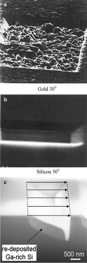
On the left of top (a), rectangle sputtered in a polycrystalline gold film at 30° angle of incidence showing the roughening of the sputtered surface relative to the unsputtered surface. On the right of top (b) a similar rectangle sputtered in a single crystal silicon surface showing that no roughening occurs [5]. On the bottom (c), redeposition during milling. Ga FIB scanning is carried out only from left to right. Thus redeposition occurs “behind” the beam. From ref. [3] (original from P. Nellen and V. Callegari, Chimia60, A735 (2006)). If the beam is scanned back and forth in both directions repeatedly, redeposition can be minimized. For a fairly deep pit as shown it will still occur and reduce the overall material removal rate by the beam, but the pit will be symmetric
-
3.
Redeposition. In certain geometries, for example when attempting to mill a very deep pit, the sputtered substrate atoms will redeposit on the sides of the pit. (This is why above we said that milling yield should be measured by milling a shallow pit.) In the case of milling of gold with gallium, the angular distribution has been measured and has the expected cosine squared dependence [8].
-
4.
Scanning speed. If the scanning speed is slow and the thickness of material removed per scan is comparable to the beam diameter, then locally under the beam the ions are not normally incident on the surface. See Fig. 8.7. This has been shown to increase the milling yield by about a factor of 2 [9].
Fig. 8.7 
(a) A schematic of the ion beam/target geometry illustrating why slow scan speed can lead to increased material removal rate. To simplify the analysis the beam was scanned rapidly in the Y direction, into the paper and advanced slowly in the X direction. If the beam is scanned slowly in both directions, the same reasoning applies but the analysis is more complex. (b) The sputter yield as a function of scan speed. Top, for Si, bottom SiO2. If the beam is scanned so slowly that each pass removes a thickness comparable to the beam diameter (as illustrated in (a)), the yield will increase. Microscopically the ions in that case are not impinging at normal incidence [9]
-
5.
Temperature of the sample can also affect the milling rate. As the thermal motion of the atoms increases, one would expect they would more readily leave the surface. But the reverse is sometimes true. At high enough temperature the sample will anneal during milling, reducing the amorphization of the surface and thus the milling yield [10]. One may also have to consider that under some circumstances the energy deposited by the ion beam may locally heat the sample, thus affecting the milling rate. Heating under the beam can be estimated by a simple calculation [11]. The conclusion is that even for an insulating substrate such as silicon dioxide the heating is minimal unless the beam diameter and beam current are large, i.e., beam heating could play a role in some circumstances.
-
6.
At low doses some swelling is observed for single crystal substrates [10]. This is due to the fact that the amorphized surface layer is less dense than the single crystal. This effect is negligible except when one is milling depths below, say, 10 nm.
-
7.
Surface contamination may also affect the rate of milling. In a moderate vacuum, like 10−6 mbar, a monolayer is adsorbed in about a second. Thus if one is scanning a relatively large area such that the average ion impingement rate per unit area is comparable to the residual gas impingement rate (5 × 10¹⁴ molecules/cm2 s), then the contamination can interfere with the removal process.


The milling yields of some typical materials are shown in Table 8.1. The numbers come from various published papers. Presumably the measurements were made for shallow pits rapidly milled and in ways that avoided the above-mentioned effects. But probably this was not the case, and there is often considerable variation in the reported numbers.
A number of workers as well as the manufacturers of the FIB/SEM systems have developed strategies and computer programs for obtaining desired shapes. For brevity we include only two references [22, 23].
8.3.2 Material Shaping Using a Precursor Gas
The precursor gas used for both adding material and enhancing the material removal is beamed onto the surface near the point of ion impact through a small needle somewhat like a hypodermic needle [3]. See Fig. 8.4. In the case of ions the chemical reaction induced by the beam can be produced by three mechanisms:
-
(a)
Collision cascades, as in the case of milling this results in energetic surface atoms which can induce chemical reactions.
-
(b)
Secondary electron emission, these low-energy electrons can also induce chemical reactions.
-
(c)
Direct ion collision with a precursor gas molecule on the surface.
Although all three mechanisms clearly can play a role, by far the dominant one in the case of gallium ions is collision cascades. (For electrons and possibly also light ion such as helium the secondary electron emission mechanism is likely dominant.)
8.3.2.1 Material Removal
The induced chemical reaction will produce material removal if the substrate is turned into a gas. For example, a commonly used gas is xenon difluoride, XeF2. It turns silicon into SiF4 which is a gas and is simply pumped away. Likewise one can think of silicon dioxide as being turned into oxygen and SiF4. Chlorine gas will act similarly. This chemical removal process proceeds in parallel with the milling. The material removal rate with gas is typically about a factor of 10 higher than without gas and with ion impact alone. Clearly for materials like gold which have no stable and volatile compounds, the removal rate cannot be enhanced with a reactive precursor gas. Table 8.2 shows some of the gases that have been used and the enhancement rates.
In addition to the increased removal rate, an important advantage of material removal with a precursor gas is that it enables one to avoid, or at least minimize, redeposition. This permits one to, for example, fabricate deeper pits with more vertical sidewalls. A second important advantage is selectivity. One can take advantage of chemistry to, for example, remove part of a film that is on top of a substrate of a different material with minimal erosion of the substrate. For example, an organic film on top of the silicon dioxide can be etched very effectively with water vapor [25]. The difference between the removal rate of the organic film and the silicon dioxide is about 20, whereas with milling alone there may be little or no difference in the removal rate.
8.3.2.2 Material Addition
The inverse process occurs when a precursor gas absorbs on the surface which has the property that the incident ion causes a volatile compound to be removed from the precursor gas molecule leaving a solid behind. For example tungsten carbonyl, W(CO)6, may dissociate into, CO, CO2, O2, C, and W. Unfortunately it turns out that both carbon and tungsten are left on the surface. Thus the “metal” left behind which is a mixture of tungsten, carbon, and gallium has a resistivity one or two orders of magnitude higher than pure tungsten. Nevertheless, this process is used for example in locally rewiring integrated circuits and in making various electrical connections in research device structures. Most of the common gases used for material deposition are organometallic, such as (Methylcyclopentadienyl) trimethylplatinum and likewise yield metal-carbon mixtures. Much purer deposits of copper and gold have been obtained by heating the substrate to temperatures of 80–100°C either by heating the entire stage [31, 32] or by locally heating the sample by focusing a laser beam near the point of ion impact [33]. In this way resistivity only about a factor of two higher than pure metal (rather than a factor of 100) can be obtained. Some examples of precursor gases and deposited materials are shown in Table 8.3. Note that also insulators such as SiO2 can be deposited. Again, the deposit is not pure. Probably largely due to the Ga ion implantation the resistivity of the oxide is lower than that of pure SiO2. Still in many cases it is a useful insulator.
An important feature of both focused ion and electron beam-induced deposition is that structures can be made on non-planar surfaces. Conventional, lithography-based fabrication, see Fig. 8.1, can only be carried out on the planar surfaces. Beam-induced deposition does not have this limitation. Within reason material can be deposited at the bottom of the pit or on the end of the pillar. A frequent application utilizing both beam milling and deposition is that a pit is cut through several layers on an integrated circuit and then filled to make electrical contact to a buried conductor. This technique is used to locally rewiring a circuit during development phase to diagnose and/or correct malfunctions.
Other examples of fabricated structures include conductors deposited on surface, Fig. 8.8b, nanocantilevers [40] Fig. 8.9, and springs [41] Fig. 8.10. The fabrication of the spring structure may seem surprising. With the beam-induced deposition, one can fabricate a cantilever extending from the edge of a cliff at some particular angle of inclination. The beam is programmed to slowly advance and material is deposited on the end of the cantilever. If the beam is advanced more slowly, the cantilever is more vertical. (If the beam is not moved at all of vertical pillar can be grown. See for example Fig. 8.17. To fabricate the spring the same principle applies except that the ion beam is programmed to slowly move in a circle and since the beam diameter is small the windings below the point on the spring being fabricated do not have any Ga+ ions incident on them, i.e., the range of the Ga ions in the wire is less than the diameter of the wire. Thus one can maintain spacing between the windings. By the way, this kind of scheme would not work with electron beams since the electron beam would penetrate through the spring winding and cause deposition on the levels below unless very low energy electrons are used.

(a) Example of FIB milled structure (30 keV Ga+ ion beam) Luthenium iron garnet (LIG) ferrimagnetic film on Gadolinium gallium garnet (GGG) [23]. (b) Microfluidics building block on silicon, FIB milled, serpentine channel with a conductor pattern on the surface fabricated by FIB-induced deposition (FEI Helios 600 FIB) photo courtesy of Jon Orloff, FEI

(a) Diamond-like carbon cantilever fabricated by FIB-induced deposition from phenanthrene C14N10 precursor gas. A 30 keV Ga+ fixed, normal incidence ion beam at 0.5 pA was used [40]. (b) Resonant spectrum of the cantilever. A small deposit made on the end of the cantilever shifts the resonant frequency. In this way a mass of 12 ± 3 × 10⁻¹⁵ g was measured

(a) A scanning electron micrograph of a spring of diamond-like carbon with 130 nm “wire” diameter [41]. It was fabricated by FIB-induced deposition from a C14N10 precursor. (b) A scanning ion micrograph of a spring 20 μm long and 130 nm wire diameter. Both were fabricated using 30 keV Ga ions at 1 pA and 5 nm beam diameter
8.4 Material Shaping with Electron Beams
In most cases, the electron beam systems used for direct material nanofabrication are simply a modified SEM. Beam diameters below 1 nm are available and a gas feed can be readily introduced. In fact, in the dual beam systems the same chamber, stage, and gas feed can be used for either electron beam or ion beam-induced processing. Electron beam-induced deposition actually predates ion beam-induced deposition. Recently electron beam-induced deposition and etching have gained technical importance because of the need to repair photomasks and EUV masks without damage due to gallium implantation. In addition electron beam-induced deposition may be favored for depositing electrical contacts on semiconductors where again damage and implantation may be undesirable.
8.4.1 Material Addition
With some exceptions the same precursor gases used with ion beams also work with electron beams. The mechanism, however, in this case is secondary electron-based. Because of their small mass and momentum, electron beams do not in general displace atoms and therefore collision cascades do not occur. Moreover, the process is less efficient. For example in many cases one molecule is dissociated per 100 incident electrons. While for ions, 10 molecules may be dissociated per incident ion. In addition, if organometallic precursors are used the large concentrations of carbon remain in the deposit and the electrical resistivity may be 4–5 orders of magnitude higher than that of pure metal. However, relatively pure deposits of gold and platinum, with the resistivities only 2–3 times higher than pure metal, have been obtained using inorganic precursor gases. However, the gold precursor AuPF3Cl is very unstable and difficult to use or obtain, and the platinum precursor Pt(PF3)4 has a low sticking coefficient and the deposition is inefficient. Limited samples of deposited materials are shown in Table 8.4. The dimensions of the deposits are larger than the beam diameter because the secondary electrons leave the surface at distances of many tens of nanometers, depending on the incident electron energy, from the point of electron impact. Note that the resistivity in Table 8.4 is given in Ω cm not μΩ cm. A far more complete listing of precursor gases and deposited materials can be found in the review article referenced earlier [3].
A nanothermometer built using electron beam-induced deposition from the organometallic platinum precursor is shown in Fig. 8.11. The resistance of this loop is a relatively sensitive to temperature so the structure can be used as a scanning probe to map the temperature of the surface [49].

Structures fabricated using electron beam-induced deposition using methylcyclopentadienyl-trimethylplatinum-platinum as a precursor gas. The structure in the top figure (a) was fabricated by tilting the stage at a given angle and keeping the beam stationary. The deposition then simply grows “up the beam.” The stages then tilted again at an appropriate angle and the new beam is grown to connect to the previous one. The curved “wires” (b, c) are grown by programming the beam to scan in an appropriate slow rate. The structure in (c) allows for four-point measurement of resistance which is more sensitive and more accurate [49]
8.4.2 Material Removal
Electron beams can also be used to remove material using precursor gas. The process is entirely gas-dependent since negligible removal occurs with electron “milling.” The secondary electrons produced by the incident beam induce a chemical reaction between adsorbed molecules and modules of the substrate leading to volatile compounds that are pumped away in the vacuum chamber. In some instances electron beams may be preferred to ion beams. Ion beams will damage whatever surface they are incident on. At the doses used here the top layer of any single crystal material will be amorphized by ions to a depth of a few hundred nanometers. Moreover, it will be heavily implanted with gallium ions. Thus in some applications like making electrical contacts to semiconductor materials or in the repair of quartz photomasks, i.e., the removal of an opaque chrome layer from the quartz, the ion damage and implantation are detrimental.
Most of the same precursor gases that are used with ion beams for material removal (Table 8.2) will also work with electron beams. It is of course necessary that the gas does not spontaneously react with the surface but rather reacts only at the point where the ion beam or in this case electron beam is incident. To be more precise, the reaction will occur in the area surrounding the point of incidence where the secondary electrons are emitted. An extensive list of precursor gases and of their applications is in the review article [3].
A technologically important challenge that has been addressed with electron beam-induced etching is the repair of lithography masks. Etchants are needed to be found for materials such as chromium and tantalum nitride [50]. (Because of the potential commercial sensitivity the etching gases have not been disclosed.) Examples of some etched structures are shown in Fig. 8.12.

Top left. Electron beam-induced etching of a chromium layer. Top right etching of a tantalum nitride layer bottom left slot X through a silicon carbide stencil mask viewed from top and bottom. Bottom right example of a freestanding bridge structure deposited across a gap [50]
An important advantage of electron beam-induced etching for mask repair is that the process can be made selective. In the case of ion beams complete selectivity is not possible because the ion beam by itself will also remove material. This selectivity is crucially important in the repair of EUV lithography masks [51]. These masks consist of delicate, thin multilayers which would be damaged by both the ion impact and the gallium implantation. An example of this kind of repair is the removal of an aluminum oxide particle using NOCl (Nitrosyl chlorine) gas. The electron beam does not induce etching of the substrate material with this precursor.
8.5 Models of Material Shaping by Ion and Electron Beams
Except for ion beam sputtering, the material removal and addition techniques depend on a precursor gas. The process can be viewed in two parts: Dynamics of the gas adsorption on the surface, and the details of the beam/solid interaction. Sputtering (ion milling) depends only on the beam solid interaction and will be discussed first.
8.5.1 Ion Sputtering
Material removal by ion bombardment is a long-standing process used in the research and industry, usually using energies between 100 and 1,000 eV. In this instance, the apparatus, usually called an ion miller, is designed to illuminate a large area, for example, an entire wafer, with the uniform current density per unit area. Patterning is achieved using photolithography, namely, covering part of the surface and leaving part of the surface uncovered to the incident ions.
There is extensive literature dating back many decades on the measurement of sputter yields of many substrates and many incident ions. See for example the three volume set, from Springer [52] and the earlier (1969) collection of data and theory [53]. In most cases, the milling yield increases monotonically with ion energy and peaks in the 50–100 keV range and then decreases.
Energetic ions entering a solid lose their energy in two ways: to the cloud of electrons, and by collisions with the nuclei in the solid. Since electrons are much, much lighter than ions. They do not perturb the path of the ions, but nevertheless, extract energy from the incident beam. The collision with the nuclei is a more random process and results in the jagged path of the incoming ion. In addition, the substrate atoms participating in the collision absorb enough energy to be launched on a path in the solid where they produce more collisions. Thus, the incoming ion produces what is called a collision cascade. This is illustrated in Fig. 8.2 on the left side.
The energy, E, loss per unit length of path, z, is written as
stopping power is defined as S(E) = −dE/dz and has, as in equation above both an electronic and nuclear complement S(E) = Sn(E) + Se(E). Both of these terms strongly depend on the mass and energy of the incident ion and the mass of the atoms in the solid. For example, a 30 keV krypton ion (close in mass to gallium) loses 10 times as much energy to nuclei (1.5 MeV/μm) than to electrons (0.15 MeV/μm). At 1,000 keV the energy loss to both ions and electrons is about the same (0.9 MeV/μm). The energy lost to the electrons generally does not alter the material while sputtering and radiation damage, i.e., amorphization of the material if it is initially single crystal, is due to the nuclear stopping power. The sputter yield is very well predicted by the Monte Carlo models developed SRIM and TRIM [54]. This is illustrated in Fig. 8.13 for nickel bombarded by a variety of ions from hydrogen, deuterium, and the noble gases. Also see Fig. 8.5 where both measured and calculated results for the relative milling yield of silicon and silicon dioxide are compared. Again, the agreement is quite good.

Comparison of measured and calculated sputter yield of nickel bombarded by a variety of ions (from [55]). The lines are drawn through the calculated points as a guide to the eye. These are broad beam measurements not FIB measurements. Still there is a fair amount of scattered in some of the measured results shown by the open symbols. But the overall trends agree fairly well
8.5.2 Surface Coverage by Precursor Gas
The precursor gas is generally delivered to the surface by capillary tube of internal diameter less than a millimeter in close proximity to the point where the ion or electron beam is incident. The geometry is shown in Fig. 8.14.

From Utke et al. [3]. The gas is delivered by capillary tube from the right as shown, and impinges on the surface over a larger area, surrounding the point of electron or ion beam incidence
In general, the ion or electron beam traverses less than a few millimeters through the precursor gas in the gas phase. As analyzed in detail [3] the probability of scattering of the incident beam by the gas molecules is negligible. The relevant interaction of the electron or ion beam with the gas occurs on (or in) the surface.
The impingement rate of molecules on the surface or the flux, J (molecules/cm2 s) at a pressure P is given by
where k is the Boltzmann constant, T the absolute temperature, and m the mass of the molecule.
For the gas used in the past for gold deposition DMG(hfac) (C7 H7F6Au) at.wt. = 434 g. At the pressures generally used, say 1 mbar, the impingement rate (or flux, J) of molecules on the surface is 7.5 × 10¹⁹ molecules/cm2 s. The impingement rate of ions (or ion flux, f) for a beam current density of 10 A/cm2 (typical for a Ga+ FIB) is 6.25 × 10¹⁹/cm2 s. Thus with a stationary beam any deposition or etching process would begin to be precursor gas limited. Moreover, one ion very likely consumes several gas molecules. (For incident electrons the situation is reversed, namely, a number of electrons are incident per dissociated molecule. However, the electron beam current density is much higher.). In fact, the situation is likely to be more complicated. An incident molecule has a certain sticking probability, s. The gas can diffuse on the surface with the diffusion coefficient, D, and a residence time, τ. Thus the density of adsorbed gas molecules on the surface as a function of radial distance from the center of the beam impingement and of time, n(r, t), is given by the following equation [3]
where σ is the cross-section for the dissociation of an adsorbed molecule, whether etching or deposition. We are assuming that at most one monolayer, characterized by a density n 0, can be adsorbed on the surface. Thus in the first term on the right hand side of the equation no more adsorption can occur if n = n 0. That only one monolayer is adsorbed on the surface at the impingement rates of interest was confirmed by experiment for the gold bearing precursor gas (DMGhfac) [56]. In steady-state the rate, R(r), as a function of distance from the center of the beam at which material is added or removed (in units of height per second) is given by
where V is the volume of material added or removed per adsorbed and dissociated molecule. The quantity f(r) is the radial distribution of incident ions measured from the center of the beam. n(r) is the steady-state solution of the differential equation above, including the impingement and adsorption of gas molecules on the surface, and their diffusion toward the point of ion impact which in effect acts as a sink for the gas molecules. The influence of diffusion of the adsorbed precursor has been experimentally observed for Cl2 on Si. A diffusion coefficient D = 8.0 × 10⁻⁶ cm2/s was measured [57].
8.5.3 Ion Beam Precursor-Gas/Solid Interaction
We have discussed the ion-solid interaction above, illustrated in Fig. 8.2. The incident ion produces a number of effects: secondary electrons are emitted, atoms are sputtered off the surface, and substrate atoms are displaced from their normal crystal sites. The dissipation of the energy of the ion in the solid can also be thought of as very locally raising its temperature. How do these effects cause gas molecules on the surface to decompose and deposit material or chemically react with the substrate leading to etching? This has been studied to some degree for deposition using noble gas ions between 2 and 10 keV [58] and up to 100 keV [59]. The results show a strong correlation between the collision cascade energy reaching the surface, (calculated by TRIM) and the dissociation rate of the adsorbed precursor gas. This is the same mechanism that causes sputtering. If a collision cascade reaches the surface and imparts sufficient energy to the surface atom, of order 5 eV, that atom will be sputtered off. However, if an adsorbed gas is present, a lower energy, say, 1 eV is all that is necessary to cause the precursor molecule to dissociate. There is, of course, competition between the addition of material due to the dissociation of the precursor gas and the removal of material due to sputtering. Since dissociation occurs at a lower energy than sputtering, deposition dominates sputtering, provided there is sufficient surface coverage by the precursor gas.
The total dissociation yield is the sum of the measured net yield for material addition, i.e., how many atoms are deposited from the precursor gas per incident ion, and the sputter yield also experimentally measured simply by turning off the precursor gas and measuring how many atoms are removed per incident ion. This total dissociation yield correlates well with the calculated yield as shown in Fig. 8.15 [58]. For each ion species there are data points at various energies between 2 and 10 keV. The slope of the line drawn through the points is adjusted by 13% (Y = 1.13X), i.e., if the correlation were perfect, we would have Y = X. This is remarkably good agreement since there were no adjustable parameters and strongly suggests that the model based on the collision cascades reaching the surface and causing the decomposition of the precursor gas is valid. In the same study the thermal spike model was also analyzed and the correlation with the yield calculated in that way was not good. It is also possible that secondary electrons emitted when the ion hits the surface can cause dissociation of the adsorbed precursor gas. However, in that instance correlation between the total dissociation yield and the secondary electron yield is completely absent.

A plot of the total decomposition yield vs. the total calculated yield using the binary collision model [58]. For each ion species, measurements were made at several energies. Thus there are several data points, i.e., the yield increased with increasing ion energy
8.5.4 Electron Beam Precursor-Gas/Solid Interaction
When an energetic electron strikes a solid surface, secondary electrons of lower energy (typically below 20 eV) are emitted. Other effects such as emission of photons or heating may also occur. But the secondary electrons play the major role in electron beam-induced deposition and etching. Because of the large difference in mass between an atom, or more precisely its nucleus, and the electron, virtually no disturbances to the lattice, such as sputtering, occur. As described in the review article [3] Monte Carlo simulations can effectively be used to model the deposition and etching. In particular the trajectories of the primary electrons and the locations where the secondary electrons are emitted can be used to model the growth of pillars. The diameters of pillars grown with a stationary electron beam in the presence of a precursor gas are always much larger than the diameter of the beam. This is due to the fact that the primary electron beam scatters in the pillar and produces secondary electrons that exit at the side of the pillar, dissociate the adsorbate, and increase the diameter. This is illustrated in Fig. 8.16. The electron trajectories can be simulated by the Monte Carlo models and the growth of surface film, as well as pillars can be predicted. As can be seen from the figure, the diameter of the pillar will be limited by the range of the primary electrons, i.e., far enough down the pillar no primary electrons will exit from the side and no secondaries will be produced.

Focused electron beam deposition due to the secondary electrons produced by the primary electrons which scatter to the side of the pillar [3]
The deleterious effects of the long electron trajectories in the solid can be avoided if deposition is carried out on an ultrathin membrane. This was in fact done and in that instance deposits, albeit very thin, with sub nanometer dimensions were produced [60].
8.6 Recent Developments
The first gallium ion beam nanofabrication was reported in the 1970s, in the decades since many practical applications have been explored and developed so that gallium ion beam nanofabrication can be thought of as a fairly mature technology.
In the past decade, four novel ion beam technologies have appeared based largely on ion source development.
8.6.1 The Gas Field Ion Source
The gas field ion source can be used to produce helium and neon ion nanobeams. The ions are produced by a cryogenically cooled, single crystal tungsten tip and are essentially emitted from a single tungsten atom. This is an exotic ion source with a long history of development. The first practical system was conceived and developed by the ALIS Corp [61]. The main application envisaged was imaging with the helium ion beam which has advantages over a conventional SEM. ALIS was acquired by Zeiss which now offers systems for sale. Nanofabrication is being explored. Typically the ion energy is about 35 keV with the beam diameter of about 1 nm and a beam current in the 1–5 pA range. Moreover, the milling yield of helium ions is very low (~0.1 atoms/ion), neon is somewhat higher. Gallium ion beams typically are in the 10 pA to 1 nA range, depending on the beam diameter desired, and have a much higher milling yield (~2–10 atoms/ion). Applications are now being explored which take advantage of the ultrasmall beam diameter and of the fact that the milling ions are inert and, unlike gallium, will not contaminate the substrate surface. Moreover, the area from which secondary electrons are emitted is smaller than for an incident electron beam, and likewise the area where collision Cascades reach the surface is likewise smaller than for gallium ions. The light helium ions impart less energy to atoms of the substrate so the straggler is more confined. Beam-induced deposition and milling have been demonstrated [42]. Some examples of fabricated structures are shown in Figs. 8.17, and 8.18. A special concern with helium ions is that they penetrate deep in the substrate resulting in trapped gas. In single crystal silicon for example macroscopic, micrometer-sized bubbles have been observed when irradiated with doses of 1.3 × 10¹⁸/cm2 at both 12 and 25 keV [62].

Pillars grown using 25 keV Helium ion beam at various currents using methylcyclopentadienyl-trimethylplatinum precursor gas [42]. Minimum pillar diameter is 36 nm

(Supplied by L. Scipioni, Carl Zeiss NTS Peabody, Ma.) Examples of milling with He ion beam. Left: A 10 nm hole drilled through an asbestos fiber. Right: A 40 nm C-shaped aperture, done by Zeiss with Stanford U. Note the sharpness of the corners
8.6.2 Plasma Ion Beam Source
Both the liquid metal gallium ion source and the cryogenic helium/neon source depend on emission from a small dot with a high current density. These sources have a high brightness. Sources based on an ionized gas are commonly used in for example, ion implanters, but are much less bright. However, they offer a very large total current, and almost any ion in the periodic table can in principle be used. If high-resolution milling is not needed and a beam diameter in the >100 nm range is acceptable, then the plasma ion source can outperform a gallium source particularly if heavy ions such as xenon are used. For example, 10 nA current can be obtained in a 300 nm diameter beam. According to simulations at a 20 μm beam diameter the xenon plasma source will deliver about two orders of magnitude more current than a gallium ion liquid metal source [63]. Plasma-based ion beam systems have been developed and are used for specific applications that require high removal rates but do not require high-resolution, for example in sectioning a solder ball in a flip chip integrated circuit as shown in Fig. 8.19 [63].

Cross-section of a 750 μm diameter solder ball used in flip chip packaging. With a 1.7 μA xenon beam this milling took 6 h. With the gallium ion beam at comparable resolution it would have taken 600 h. The image was also taken with a xenon beam but at the 100 pA where the resolution (beam diameter) is about 80 nm. The dark and light areas show crystal grains. This kind of sectioning is useful in diagnosing solder ball/substrate contact problems (image courtesy of Noel Smith, Oregon Physics, Hillsboro Oregon)
8.6.3 Laser Cooled Source
Laser radiation is used to cool atoms trapped in a magnetic field. The ion temperature can be reduced to the millikelvin range. Thus when they are ionized and extracted the energy spread is small permitting finer focus by minimizing chromatic aberration. Atomic spectral lines have to be matched to the laser wavelength. Most recently Li ion beams have been reported [64]. This is an exciting development but is still in the research stage.
8.6.4 Multibeam Ion Sources
One of the main shortcomings of FIBs (and electron beams) is the slow rate of material removal or addition. They are mainly used for local, single structure fabrication. Multiple beam systems for both ions and electrons have been developed in the past years. The systems are largely aimed at lithography, namely, exposure of resist. The systems use a plasma ion source to produce a relatively broad beam of collimated ions which are incident on a stencil mask that can have a static pattern of openings or programmable windows which allow complex patterns to be written [65]. These multibeam systems of either ions or electrons would be useful in instances where the intended fabrication is over a large area so that many sites can be addressed simultaneously. Obviously the systems are not suitable if one wants to make, for example, a single pit in the sample.
Figure 8.20 shows examples of structures milled in a nickel film with a 10 keV argon beams in a multibeam machine [66]. A silicon stencil mask with the pattern over a 5 mm × 5 mm area is back illuminated with a broad, collimated argon ion beam. The pattern passes through ion optics where it is demagnified 200 times resulting in a field size of 25 × 25 μm projected on the sample. The current density on the sample was 110 μA/cm2 and the features shown in both parts of the figure are milled to a depth of 80 nm in 19 s. These patterns are used in a conventional injection molding machine to produce the reverse patterns in polymer materials. The patterns were produced with a static stencil mask. Programmable masks have also been produced which can direct and control 43,000 individual beams on the sample for writing more intricate, customized patterns. However, for this kind of patterning with a programmable mask rather than a fixed stencil mask the milling time would be much longer because the total window area in the programmable mask is much smaller than in the static mask. Considerable area is required to accommodate the switching circuitry, so that only about 1% of the ion current incident on the mask passes down to the sample. On the other hand, the static mask is exactly as shown in Fig. 8.20 enlarged 200 times, and has a large open area.

Hexagons with 470 nm diagonal diameter and the minimum spacing of 100 nm milled in nickel to a depth of 80 nm and an array of circular holes with a diameter of 150 nm milled into a nickel surface to a depth of 80 nm [66]
8.7 Beam Patterning in the Volume
The fabrication with ion and electron beams that we have discussed so far could be characterized as surface fabrication either material is removed from the surface or deposited on the surface. The beams can also produce chemical or physical changes in the volume of the material. This can also be exploited in nanofabrication. The standard exposure of resist, as in e-beam lithography, is an example of a chemical change produced by the beam. In addition, ion beams can produce physical change in the volume in the form of damage or local amortization. This can then be exploited in preferential etching, or resistance to etching. In addition, the presence of the implanted ions can also physically alter the material. For example, silicon implanted with the helium nanobeam discussed above can form bubbles [62]. See Fig. 8.21.

From ref. [62]. Cross-section of silicon sample implanted with a helium ion dose of 1.3 × 10¹⁸ ions/ cm2 at beam energies of (a) 12 keV and (b) 25 keV. A 2 μm × 2 μm area was exposed. Evidently the helium is not soluble in silicon and forms a bubble. Note that the bubble skin thickness is related to the ion penetration depth. At higher energy the bubble starts the form deeper in the substrate
If a resist has good mechanical and chemical stability, it can itself present a useful structure. For example, an epoxy-based resist called SU8-2000 exposed with a 5 keV electron beam has been used to produce photonic waveguides down to 100 nm [67].
High-energy, MeV proton beams have also been used to produce high aspect ratio structures in materials such as SU8. The advantage of the proton beam is that it can penetrate many tens of micrometers in material and alter the material along a straight line trajectory. This allows one to produce high aspect ratio structures, for example, 60 nm structures, 10 μm deep in SU8. For the review of this work, see ref. [68].
8.8 Conclusions
Focused ion and electron beams can be used to fabricate structures down into the 10 nm regime. Both material removal and material addition are possible. With ion beams, material can be removed by sputtering and by sputtering in the presence of a reactive gas which can greatly increase the removal rate. Material can be added by flooding the sample surface with an appropriate precursor gas which the ion beam dissociates to leave a deposit behind. With electron beams material can only be removed with the aid of a reactive gas. And material can be added with the aid of a precursor gas. However, since these are point beams, fabrication is slow. So in general they can be used only for limited volumes. For example, to mill a volume of 1 μm3 with a 10 pA beam would take 5 min. By sacrificing resolution one can increase the current and decrease the milling time by as much as two orders of magnitude the minimum dimensions at which structures can be fabricated is larger than the beam diameter, often hundred nanometers, rather than the 1–10 nm ion or electron beam diameter. This is because the ion-surface interaction produces collision cascades some distance from the point of ion impact. Similarly electron-surface interaction causes secondary electrons to be emitted from an area surrounding the point of impact.
Much of the impetus for the development of the systems has come from the semiconductor industry where they are used for mask repair, for sample sectioning for failure analysis, and for circuit rewiring. However, many other nanofabrication applications have been demonstrated in diverse fields. Recent developments promise even finer resolution fabrication with helium or neon ions, rapid fabrication with xenon ion plasma sources, and multibeam fabrication with potential manufacturing applications.
References
Thompson LF, Willson CG, Bowden MJ (1994) Introduction to microlithography, 2nd edn. ACS, Washington, DC
Orloff J, Utlaut M, Swanson L (2003) High resolution focused ion beams: FIB and its applications. Springer, New York
Utke I, Hoffmann P, Melngailis J (2008) J Vac Sci Technol B 26(4):1197
http://portal.tugraz.at/portal/page/portal/felmi/research/FIB/Principles%20of%20FIB
Xu X, DellaRatta AD, Sosonkina J, Melngailis J (1992) J Vac Sci Technol B 10(6):2675
TRIM (or SRIM) simulation of sputtering: http://www.srim.org/
Muller KP, Petzold HC (1990) Proc SPIE 1263:12
Santamore D, Edinger K, Orloff J, Melngailis J (1997) J Vac Sci Technol B 15(6):2346
Lugstein A, Steiger-Thirsfeld A, Basnar B, Hyun YJ, Pongratz P, Bertagnolli E (2009) J Appl Phys 105(4):044912
Melngailis J (1987) J Vac Sci Technol B 5(2):469
Yamaguchi H (1987) J Phys Colloques 48(C6):165
Muller KP, Petzold HC (1990) Proc SPIE 1263(12) (repeat with [8])
Anderson HH, Bay HL (1981) Topics in applied physics: sputtering by particle bombardment. In: Behrisch R (ed) Physical sputtering of single element solids, vol 47. Springer, New York, p 145
Young RJ, Cleaver JRA, Ahmed H (1993) J Vac Sci Technol B 11(6):234
Adams DP, Vasile MJ, Mayer TM, Hodges VC (2003) J Vac Sci Technol B 21(6):2334
Stanishevsky A (2001) Thin Solid Films 398:560
Steckl AJ, Chyr I (1999) J Vac Sci Technol B 17(2):362
Blauner PG, Ro JS, Butt Y, Melngailis J (1989) J Vac Sci Technol B 7(4):609
Ostadi H, Jiang K, Prewett PD (2009) Microelectron Eng 86(4):1021
Mulders JJL, de Winter DAM, Duinkerken WJHCP (2007) Microelectron Eng 84(5):1540
Vasile MJ, Xie J, Nasser R (1999) J Vac Sci Technol B 17(6):3085
Vick D, Sauer V, Fraser AE, Freeman MR, Hiebert WK (2010) J Micromech Microeng 20(10):105005
Ochiai Y, Gamo K, Namba S, Shihoyama K, Masuyama A, Shiokawa T, Toyoda K (1987) J Vac Sci Technol B 5(1):423
Stark TJ, Shedd GM, Vitarelli J, Griffis DP, Russell PE (1995) J Vac Sci Technol B 13(6):2565
Young RJ, Cleaver JRA, Ahmed H (1993) J Vac Sci Technol B 11(2):234 (repeat with [17])
Harriott LR (1993) J Vac Sci Technol B 11(6):2012
Kola RR, Celler GK, Harriott LR (1993) Mater Res Soc Symp Proc 279:593
Edinger K (1999) J Vac Sci Technol B 17(6):3058
Santschi C, Jenke M, Hoffmann P, Brugger J (2006) Nanotechnology 17(11):2722
DellaRatta AD, Melngailis J, Thompson CV (1993) J Vac Sci Technol B 11(6):2195
Blauner PG, Butt Y, Ro JS, Thompson CV, Melngailis J (1989) J Vac Sci Technol B 7(4):1816
Funatsu J, Thompson CV, Melngailis J, Walpole JN (1996) J Vac Sci Technol B 14(1):179
Stewart DK, Stern LA, Morgan JC (1989) Proc SPIE 1089:18
Luxmoore IJ, Ross IM, Cullis AG, Fry PW, Orr J, Buckle PD, Jefferson JH (2007) Thin Solid Films 515(17):6791
Tao T, Ro JS, Melngailis J, Xue Z, Kaesz HD (1990) J Vac Sci Technol B 8(6):1826
Puretz J, Swanson LW (1992) J Vac Sci Technol B 10(6):2695
Gannon TJ, Gu G, Casey JD, Huynh C, Bassom N, Antoniou N (2004) J Vac Sci Technol B 22(6):3000
Edinger K, Melngailis J, Orloff J (1998) J Vac Sci Technol B 16(6):3311
Igaki J, Nakamatsu K, Kometani R, Kanda K, Haruyama Y, Kaito T, Matsui S (2006) J Vac Sci Technol B 24(6):2911
Namatsu K, Nagase M, Igaki J, Namatsu H, Matsui S (2005) J Vac Sci Technol B 23(6):2801
Alkemade PFA, Chen P, Veldhoven EV, Maas D (2010) J Vac Sci Technol B 28(6):C6F22
Hoyle PC, Cleaver JRA, Ahmed H (1996) J Vac Sci Technol B 14(2):662
Koops HWP, Weiel R, Kern DP, Baum TH (1988) J Vac Sci Technol B 6(1):477
Utke I, Dwir B, Leifer K, Cicoira F, Doppelt P, Hoffmann P, Kapon E (2000) Microelectron Eng 53(1):261
Yavas O, Ochiai C, Takai M, Park YK, Lehrer C, Lipp S, Frey L, Ryssel H, Hosono A, Okuda S (2000) J Vac Sci Technol B 18(2):976
Barry JD, Ervin M, Molstad J, Wickenden A, Brintlinger T, Hoffman P, Meingailis J (2006) J Vac Sci Technol B 24(6):3165
Utke I, Hoffmann P, Dwir B, Leifer K, Kapon E, Doppelt P (2000) J Vac Sci Technol B 18(6):3168
Edinger K, Gotsalk T, Rangelow I (2001) J Vac Sci Technol B 19(6):2856
Edinger K, Becht H, Bihr J, Boegli V, Budach M, Hofmann T, Koops HWP, Kuschnerus P, Oster J, Spies P, Weyrauch B (2004) J Vac Sci Technol B 22(6):2902
Bret T, Afra B, Becker R, Hofmann T, Edinger K, Liang T, Hoffmann P (2009) J Vac Sci Technol B 27(6):2727
Behrisch R (ed) (1981, 1983) Topics in applied physics “Sputtering by particle bombardment,” vol 52, 47; Behrisch R, Wittmaak K (eds) (1991) Topics in applied physics “Sputtering by particle bombardment,” vol 64. Springer Verlag, Berlin; also Behrisch R, Eckstein W (eds) ((2007)) Topics in applied physics, Sputtering by particle bombardment: experiments and computer calculations, vol 110. Springer, Berlin
Carter G, Colligon JS (1969) Ion bombardment of solids. Heinemann, London
Ziegler JF, Biersack JP, Littmark U (1984) The stopping and range of ions in solids, vol. 1 of series stopping and ranges of ions in matter. Pergamon Press, New York, see also http://www.srim.org/
Biersack JP, Eckstein W (1984) Appl Phys A 34(2):73
Dubner AJ, Wagner A (1989) J Appl Phys 66(2):870
Harashi S, Komoro M (1993) Jpn J Appl Phys 32:6168
Dubner AJ, Wagner A, Melngailis J, Thompson CV (1991) J Appl Phys 70(2):665
Ro JS, Thompson CV, Melngailis J (1994) J Vac Sci Technol B 12(1):73
van Dorp WF, Lazić I, Beyer A, Gölzhäuser A, Wagner JB, Hansen TW, Hagen CW (2011) Nanotechnology 22(11):115303
Ward BW, Notte JA, Economou NP (2006) J Vac Sci Technol B 24(6):2871
Livengood R, Tan S, Greenzweig Y, Notte J, McVey S (2009) J Vac Sci Technol B 27(6):3244
Tesch P, Smith N, Martin N, Kinion D (2008) Proceedings of the 34th ISTFA conference, vol 7
Knufman B, Steele AV, Orloff J, McClelland JJ (2011) New J Phys 13(10):103035
Platzgummer E, Loeschner H (2009) J Vac Sci Technol B 27(6):2707
Koeck A, Bruck R, Wellenzohn M, Hainberger R, Platzgummer E, Loeschner H, Joech P, Eder-Kapl S, Ebm C, Czepl P et al (2010) J Vac Sci Technol B 28(6):C6B2
De Vittorio M, Todaro MT, Stomeo T, Cingolani R, Cojoc D, Di Fabrizio E (2004) Microelectron Eng 73:388
Watt F, Breese MBH, Bettiol AA, van Kan JA (2007) Mater Today 10(6):20
Author information
Authors and Affiliations
Corresponding author
Editor information
Editors and Affiliations
Rights and permissions
Copyright information
© 2013 Springer Science+Business Media New York
About this chapter
Cite this chapter
Melngailis, J. (2013). Material Shaping by Ion and Electron Nanobeams. In: Hocheng, H., Tsai, HY. (eds) Advanced Analysis of Nontraditional Machining. Springer, New York, NY. https://doi.org/10.1007/978-1-4614-4054-3_8
Download citation
DOI: https://doi.org/10.1007/978-1-4614-4054-3_8
Published:
Publisher Name: Springer, New York, NY
Print ISBN: 978-1-4614-4053-6
Online ISBN: 978-1-4614-4054-3
eBook Packages: EngineeringEngineering (R0)