
Abstract
Dielectrics are an important class of thin-film electronic materials for microelectronics. Applications include a wide swathe of device applications, including active devices such as transistors and their electrical isolation, as well as passive devices, such as capacitors. In a world dominated by Si-based device technologies, the properties of thin-film dielectric materials span several areas. Most recently, these include high-permittivity applications, such as transistor gate and capacitor dielectrics, as well as low-permittivity materials, such as inter-level metal dielectrics, operating at switching frequencies in the gigahertz regime for the most demanding applications.
This chapter provides a survey of the various dielectric material systems employed to address the very substantial challenge associated with the scaling Si-based integrated circuit technology. A synopsis of the challenge of device scaling is followed by an examination of the dielectric materials employed for transistors, device isolation, memory and interconnect technologies. This is presented in view of the industry roadmap which captures the consensus for device scaling (and the underlying economics) – the International Technology Roadmap for Semiconductors. Portions of the survey presented here are selected from work previously published by the author [28.1,2,3].
Access provided by Autonomous University of Puebla. Download reference work entry PDF
Keywords
- Electron Spin Resonance
- Chemical Mechanical Polishing
- Gate Electrode
- Barium Strontium Titanate
- Capacitance Density
These keywords were added by machine and not by the authors. This process is experimental and the keywords may be updated as the learning algorithm improves.
This chapter considers the role of dielectric materials in microelectronic devices and circuits and provides a survey of the various materials employed in their fabrication. We will examine the impact of scaling on these materials, and the various materials utilized for their dielectric behavior. Extensive reviews are available on the device characteristics for the reader to consult [28.4,5,6,7]. We will primarily confine the discussion here to Si-based microelectronic circuits.
Dielectric materials are an integral element of all microelectronic circuits. In addition to their primary function of electrical isolation of circuit and device components, these materials also provide useful chemical and interfacial properties. The material (and resulting electrical) properties of dielectrics must also be considered in the context of the thin films used in semiconductor microelectronics, as compared to bulk properties. The dimensions of these dielectric thin films are determined by the device design of the associated integrated circuit technology, and these dimensions decrease due to a calculated design process called scaling.
FormalPara 28.0.1 The Scaling of Integrated CircuitsThe ability to reduce the size of the components of integrated circuits (ICs), and therefore the circuits themselves, has resulted in substantial improvements in device and circuit speeds over the last 30 years. Equally important, this calculated size reduction permits the fabrication of a higher density of circuits per unit area on semiconductor substrates. The economic implication of this scaling was captured by G. Moore more than 40 years ago [28.8].
- Mooreʼs Law:
-
Moore observed that the minimum cost of manufacturing integrated circuits per component actually decreases with increasing number of IC components, and thus with greater circuit functionality and computing power. This is obviously an important economic driving force, as the ability to increase the number of circuits per unit area would lead to a lower minimum cost, and thus higher market demand and more potential profit. Moreover, Moore noted that the rate of increase in the number of components for a given circuit function roughly doubled each year in the early 1960s, and predicted that it would continue to do so through 1975. In 1975, Moore revised this estimate of doubling time to 24 months due to the anticipated complexity of circuits [28.9].
The semiconductor industry has generally confirmed (and aligned to meet) these extrapolations, often referred to as Mooreʼs law, over the last 30 years. The extrapolation is often analyzed in the semiconductor industry, and the doubling period, which has varied between 17 and 32 months over the life of the industry, is now roughly 23 months [28.10]. Indeed the cost per transistor has decreased from ≈5 $/ transistor in 1965 to less than 10−6 $/transistor today [28.11]. Current advanced Si IC production technology results in the fabrication of well over 500000000 transistors on a microprocessor chip.
- Technology Roadmap:
-
The contemporary industry analysis encompassing this observation is presented in the International Technology Roadmap for Semiconductors (ITRS) where the extrapolations of the future technological (and economic) requirements for the industry are annually updated [28.12]. The current scaling trends indicate that the compound annual reduction rate (CARR) in device dimensions is currently consistent with the following equation:
 (28.1)
where T is the technology node cycle time measured in years. Thus in two years, the rate of reduction is −15.9%. This corresponds to a scaling factor of ≈0.7 × from a given technology node to the next, or a factor of ≈0.5 × over the time of two technology nodes. Recent reviews and predictions for the limits of scaled integrated circuit technology continue to be available [28.13,14].
Table 28.1 provides selected scaling targets from the ITRS through 2010 [28.12]. As may be seen, the industry roadmap now segregates scaling targets among three categories: microprocessor (MPU)/application-specific IC (ASIC) applications, low-operational-power applications, and low-stand-by-power applications. Higher-performance technologies, such as MPU/ASIC applications, require aggressive scaling, while low-stand-by-power applications require less-aggressive scaling. A key criteria to enable these technologies is the associated power management in the on and off state, hence leakage current remains an important distinction amongst the various roadmap applications.
Table 28.1 Selected scaling targets from the ITRS roadmap [28.12] - Performance and Scaling:
-
The concomitant reduction in device dimensions, such as transistor channel length, associated with increasing the number of components per unit area has resulted in a significant increase in processing performance – the speed at which computations can be done. For example, as scaling reduces the distance that carriers must travel in a transistor channel, the response time of the transistor as a digital switch also decreases (as long as sufficient mobility is maintained). Scaling has resulted in the speeds of microprocessors increasing from 25–50 MHz clock frequencies in the early 1990s (≈106 transistors) to 2.2 GHz in 2003 (≈108 transistors) [28.15]. Current predictions suggest that 20-GHz frequencies are possible for complementary metal oxide semiconductor (CMOS)-based microprocessors incorporating 109 transistors [28.11].
The various dielectric materials associated with the components impacts the overall performance of the corresponding IC technology. In the case of transistors, the gate dielectric is integral to the performance of transistor electrical characteristics such as the drive current I d. The interconnection performance of circuit elements is influenced by the dielectric material that isolates the various metal interconnection lines through the line-to-line capacitance. Memory elements incorporate very-low-leakage dielectric materials for charge-storage purposes. The behavior of these materials with component size reduction is thus an important design consideration in IC technology.
Figure 28.1 shows the dependence of the delay time as a function of technology node (scaling) associated with conventional CMOS transistor gates interconnected with metal lines that are isolated with different dielectrics [28.16]. The total delay time associated with the circuit response for a given technology node is a combination of the temporal response of the transistor gate (influenced by the gate capacitance) as well as the propagation through the interconnecting wire lines associated with the circuit [influenced by the wire resistance and the line-to-line capacitance, i.e. a resistive–capacitive (RC) delay] [28.16,17]. Changing both the interconnect wire material (from Al to Cu) to decrease the line resistivity as well as decreasing the dielectric constant in the material isolating these lines (from SiO2 to a lower dielectric constant material) to decrease line-to-line parasitic capacitance minimizes the overall RC delay time response. Of course, the challenge in adopting this solution was the successful integration of these material changes into a high-volume fabrication line, which took the investment of considerable time and effort.
Fig. 28.1 
Time delay contributions for integrated circuits. The resultant delay is dependent upon the circuit architecture as well as the material constituents. After [28.16] (© 2004 IEEE, with permission)
In order to compare the performance of different CMOS technologies, one can consider a performance metric that captures the dynamic response (i.e. charging and discharging) of the transistors associated with a specific circuit element to the supply voltage provided to the element at a representative (clock) frequency [28.1,18,19]. A common element employed to examine such switching-time effects in a new transistor design technology node is a CMOS inverter. This circuit element is shown in Fig. 28.2 where the input signal is attached to the gates and the output signal is connected to both the n-type MOS (NMOS) and p-type MOS (PMOS) transistors associated with the CMOS stage. The switching time is limited by both the fall time required to discharge the load capacitance by the n-type field-effect transistor (n-FET) drive current and the rise time required to charge the load capacitance by the p-FET drive current. That is, the switching response times τ are given by:
 (28.2)
and C j and C i are the parasitic junction and local interconnection capacitances, respectively. Of course, as one considers the combination of transistors to produce various circuit logic elements to enable computations (viz. a processor), it is also clear that the manner in which the transistors are interconnected also plays an important role on the overall performance of the circuit. The fan out for interconnected devices is given by the factor F. Ignoring delay in the gate electrode response, as τ GATE ≪ τ n,p, the average switching time is therefore:
 (28.3)
Fig. 28.2 
Example circuits employed to evaluate the performance of a transistor technology. For example, elements are combined to simulate processor performance adequately. After [28.1] (AIP, with permission© 2001)
The load capacitance in the case of a single CMOS inverter is simply the gate capacitance if one ignores parasitic contributions such as junction and interconnect capacitance. Hence, an increase in I d is desirable to reduce switching speeds. For more realistic estimates of microprocessor performance, the load capacitance is connected (fanned out) to other inverter elements in a predetermined fashion. When coupled with other NMOS/PMOS transistor pairs in the configuration shown in Fig. 28.2, one can create a logic NAND gate, which can be used to investigate the dynamic response of the transistors and thus examine their performance under such configurations. For example, a fan out F = 3 can be employed in microprocessor performance estimates, as shown in Fig. 28.2.
One can then characterize the performance of a circuit technology (based on a particular transistor structure) through this switching time. To do this, various figures of merit (FOM) have been proposed that incorporate parasitic capacitance as well as the influence of gate sheet resistance on the switching time [28.18,19,20]. For example, a common FOM employed is related to (28.3) simply by
 (28.4)
In the case where parasitic capacitance and resistance effects are ignored, it is easily seen then that an increase in the device drive current I d results in a decrease in the switching time and thus an increase in the FOM value (performance). However, the incorporation of parasitic effects results in the limitation of FOM improvement, despite an increase in the gate dielectric capacitance. All of these issues depend critically upon the materials constituents of the integrated circuit, and dielectrics are an important component [28.1].
- Impact of Scaling on Dielectrics:
-
The scaling associated with the device dimensions that constitute an integrated circuit impacts on virtually all film dimensions such as thickness, including the dielectrics employed in the circuit. Various scaling methodologies have been applied since the pioneering work by Dennard and coworkers [28.21,22]. These various methods have been recently summarized [28.5,23]. For example, following the work by Dennard et al., the scaling of the transistor from one node N to the next N + 1 under a constant-electric-field condition would result in a relationship between the new transistor gate (or channel) length L N+1 = L N /α, where α > 1 is the constant scaling factor (Fig. 28.3). Other dimensions, such as the gate dielectric thickness and the gate width, scale similarly. The voltage would also scale according to V N+1 = V N /α in this scenario as well. Table 28.1 provides the drive voltage scaling (V dd) anticipated by the ITRS roadmap, depending upon the application.
Fig. 28.3 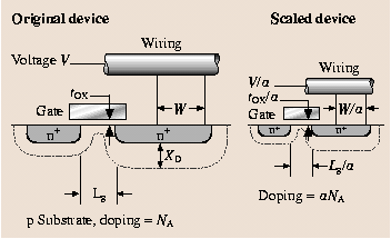
Scaling methodology for integrated circuit technology. After [28.23] (© 2004 IEEE, with permission)
This scaling approach has several shortcomings, including the reduction of power-supply voltages with each node, raising problems with circuit power-supply compatibility. So, for earlier technology nodes (L ≥0.35 μm), the power supply was kept constant while the device dimensions were scaled as described above. Eventually, the resultant higher electric fields associated with this scaling approach led to reliability concerns for the gate dielectric, mobility degradation and hot-carrier effects. For further scaling, the power supply was scaled at a different factor (such as α 1/2) to compensate for such effects. For modern devices with deep-submicron gate length, other techniques are used to scale from node to node. Nevertheless, for CMOS technology over the last ≈ 25 years, it has been noted that the gate dielectric thickness can be related to the channel length as shown in Fig. 28.4 for a wide variety of device technologies [28.24].
Fig. 28.4 
Scaling trends of the transistor gate length and the gate insulator thickness for various generations of integrated technologies. The solid line is a linear fit to the data. The dashed line represents the approximate scaling trend between the gate dielectric thickness and gate length observed over several technology generations: L G = 45 × t ox. After [28.24], with permission
The critical point in the context of dielectric films is that the dimensions of the devices, and therefore the dimensions (thicknesses) of the dielectric layers, are significantly reduced as scaling proceeds (Table 28.1). At some point, the materials properties associated with the dielectric in a component will be predicted to no longer provide the desirable electrical behavior attained in previous nodes, thus stimulating research on new dielectric materials. In the case of gate dielectrics, scaling results in thinner layers to a point where quantum-mechanical tunneling becomes an issue. For memory capacitor dielectrics, a specific capacitance density is required, regardless of capacitor dimensions, for a reliable memory element. Indeed, scaling impacts on the selection and integration of numerous constituents of electronic devices including gate electrode materials, source/drain junction regions, contacts, interconnect dielectrics.


Dielectrics are pervasive throughout the structure of an integrated circuit. Applications include gate dielectrics, tunneling oxides in memory devices, capacitor dielectrics, interconnect dielectrics and isolation dielectrics, as well as sacrificial or masking applications during the circuit fabrication process.
The basic properties utilized in dielectric materials include their structure and the resultant polarizability behavior. As noted in Fig. 28.5, there are several mechanisms to consider in the polarization of materials in the presence of an electric field. For nonmetallic (insulating) solids in CMOS applications, there are two main contributions of interest to the dielectric constant which give rise to the polarizability: electronic and ionic dipoles. Figure 28.5 illustrates the frequency ranges where each contribution to the real part of the complex relative dielectric permittivity ε r dominates, as well as the imaginary part of the complex permittivity (dielectric losses), ε r′′ [28.25]. The region of interest to CMOS applications includes the shaded area where switching frequencies are in the GHz range at the present time.

Schematic of the dependence of dielectric permittivity on frequency. After [28.25], with permission
In general, atoms with a large ionic radius (i.e. high atomic number, Z) exhibit more electron dipole response to an external electric field, because there are more electrons to respond to the field (electron screening effects also play a role in this response). This electronic contribution tends to increase the permittivity of materials with higher-Z atoms.
The ionic contribution to the permittivity can be much larger than the electronic portion in cases such as perovskite crystals of (Ba,Sr)TiO3 (BST) and (Pb,Zr)TiO3 (PZT), which exhibit ferroelectric behavior below the Curie point. In these cases, Ti ions in unit cells throughout the crystal are uniformly displaced in response to an applied electric field (for the case of ferroelectric materials, the Ti ions reside in one of two stable, non-isosymmetric positions about the center of the Ti–O octahedra). This displacement of Ti ions causes an enormous polarization in the material, and thus can give rise to very large dielectric constants in bulk films of 2000–3000, and has therefore been considered for dynamic random-access memory (DRAM) capacitor applications [28.26,27]. Since ions respond more slowly than electrons to an applied field, the ionic contribution begins to decrease at very high frequencies, in the infrared range of ≈1012 Hz, as shown in Fig. 28.5.
Gate Dielectrics
Transistor Structure
A cross-sectional schematic of the structure of a metal–oxide–semiconductor (MOS) field-effect transistor (FET) and a modern CMOS transistor, consisting of the n-FET and p-FET pair, is shown in Fig. 28.6. The source- and drain-region dopant profiles reflect modern planar CMOS technologies where an extended, doped region is produced under the gate region in the channel. Additionally, so-called halo or pocket dopant implantation regions are also shown. These dopant profile approaches have been incorporated in recent years in an effort to permit transistor channel scaling and yet maintain performance [28.28].

Important regions of (a) a MIS field-effect transistor, and (b) a planar CMOS transistor structure. After [28.31] (© 2004 IEEE, with permission)
As can be seen, there exist several regions of the device which require dielectric materials to enable useful transistor operation. Both n-MOS and p-MOS transistors are isolated with a dielectric, typically deposited SiO2 in most modern device technologies, which is deposited in trench structures. This isolation technique is called shallow trench isolation (STI) as the associated trench depth is ≤0.5 μm. Earlier generations of CMOS (and often devices under research) also utilized the so-called local oxidation of silicon (LOCOS) isolation approach [28.29,30]. So-called spacer dielectrics (typically SiO2, SiO x N y , or SiN x ) are also used around the transistor gate stack for isolation and implantation-profile control. The gate stack is defined here as the films and interfaces comprising the gate electrode, the underlying gate dielectric, and the channel region. The gate dielectric, typically SiO2 or SiO x N y for transistors currently in production, electrically isolates the gate electrode from the underlying Si channel region while allowing the modulation of the carrier flow in the channel. As we shall see, the interface between the gate dielectric and the channel regions is particularly important in regard to device performance.
Transistor Dielectric Requirements in View of Scaling
In addition to the thickness reduction associated with scaling, the gate dielectric must adhere to several requirements that are dependent upon the specific product application, including adequate drive current, suitable capacitance, minimal leakage current, and reliable performance. Table 28.1 provides some selected values describing the ITRS 2003 roadmap.
Drive Current
The improved performance associated with the scaling of logic device dimensions can be seen by considering a simple model for the drive current associated with a FET [28.1,3,18,20]. In the gradual channel approximation, the drive current can be written as:

where W is the width of the transistor channel, L is the channel length, μ is the channel carrier mobility (assumed to be constant in this analysis), C inv is the capacitance density associated with the gate dielectric when the underlying channel is in the inverted state, V G and V D are the voltages applied to the transistor gate and drain, respectively, and the threshold voltage is given by V T. It can be seen that in this approximation the drain current is proportional to the average charge across the channel (with a potential V D/2) and the average electric field (V D/L) along the channel direction. Initially, I D increases linearly with V D and then eventually saturates to a maximum when V D,sat = V G − V T to yield:

A goal here is to increase the saturation drive current as much as possible for a given transistor technology design. The term (V G − V T) is limited in range due to reliability concerns as too large a V G would create an undesirable, high electric field across the gate dielectric. Moreover, practical operation of the device at room temperature (or above) requires that V T cannot easily be reduced below about 8 × k B T ≅200 meV (k B T ≈25 meV at room temperature). Elevated operating temperatures could therefore cause statistical fluctuations in thermal energy, which would adversely affect the desired V T value. Thus, even in this simplified approximation, one is left to pursue a reduction in the channel length, increasing the width, increasing the gate dielectric capacitance, or a carefully engineered combination of all of these in order to increase I D,sat. Note that none of these dimensions are, in reality, independent and so substantial resources are utilized to simulate device performance in order to maximize the performance prior to the fabrication of a representative transistor [28.5,30,32].
Gate Capacitance
In the case of increasing the inversion capacitance to improve I D, consider the gate stack structure idealized as a parallel-plate capacitor (ignoring quantum-mechanical and depletion effects from a Si substrate and gate [28.33]),

where κ is the dielectric constant of the material, ε 0 is the permittivity of free space (=8.85×10⁻³ fF/μm), A is the area of the capacitor, and t is the thickness of the dielectric between the capacitor electrode plates. (Note that the relative permittivity of a material is often given by ε or ε r, such as with the expression C = εε 0 A/t. Note that the relation between κ and ε varies depending on the choice of units (e.g. when ε 0 = 1), but since it is always the case that κ ≈ ε, we shall assume here that κ = ε.) It is clear that transistor designs utilizing planar CMOS scaling approaches discourage increasing the area of the capacitor, and so one is left to considering the reduction of the dielectric thickness in order to increase the capacitance.
In order to compare alternative dielectric materials which exhibit a dielectric constant higher than the standard for the industry, SiO2, this expression for C can also be rewritten in terms of t eq (i.e. equivalent oxide thickness) and th eκ ox of the capacitor (κ ox =3.9 for the low-frequency dielectric constant of SiO2). The term t eq then represents the theoretical thickness of SiO2 that would be required to achieve the same capacitance density as the dielectric (ignoring important issues such as leakage current and reliability). For example, if the capacitor dielectric is SiO2, t eq =3.9 ε 0(A/C), and so a capacitance density of C/A =34.5 fF/μm2 corresponds to t eq =10 Å.
Thus, the physical thickness of an alternative high-κ dielectric employed to achieve the equivalent capacitance density of t eq =10 Å can be obtained from the expression

From this expression, a dielectric with a relative permittivity of 16 therefore results in a physical thickness of ≈40 Å, to obtain t eq =10 Å. The increase in the physical thickness of the dielectric impacts on properties such as the tunneling (leakage) current through the dielectric, and is discussed further below.
The industry scaling process clearly presents a major challenge for the core transistor gate dielectric as predictions call for a much thinner effective thickness for future alternative gate dielectrics: t eq ≤1 nm [28.12]. The interfacial regions between the gate electrode, dielectric and channel [in totality termed the metal–insulator–semiconductor (MIS) gate stack as shown schematically in Fig. 28.7] require careful attention, as they are particularly important in regard to transistor performance. These regions, less than approximately 0.5 nm thick, serve as a transition between the atoms associated with the materials in the gate electrode, gate dielectric and Si channel, and can alter the overall capacitance of the gate stack, particularly if they have a thickness that is substantial relative to the gate dielectric. Additionally, these interfacial regions can be exploited to obtain desirable properties. The upper interface, for example, can be engineered in order to block boron out-diffusion from the poly-Si gate. The lower interface, which is in direct contact with the CMOS channel region, must be engineered to provide low interface trap densities (e.g. dangling bonds) and minimize carrier scattering (maximize channel carrier mobility) in order to obtain reliable, high-performance device. Mobility degradation, relative to that obtained using SiO2 (or SiON) gate dielectrics, associated with the incorporation of high-κ gate dielectrics is an important issue currently under investigation and discussed further below.

Schematic of the important regions of the transistor gate stack. After [28.1] (AIP, with permission © 2001)
Reactions at either of these interfaces during the device fabrication process can result in the formation of a significant interfacial layer that will likely reduce the desired gate stack capacitance. Additionally, any suitable interfacial layer near the channel must result in a low density of electrically active defects (⪅1011/ cm2eV is often obtained for SiO2) and avoid degradation of carrier mobility in the region near the surface channel.
The reduced capacitance can be seen by noting that the dielectric film that has undergone interfacial reactions results in a structure that essentially consists of several dielectric layers in series. If we suppose that the dielectric consists of two layers, then from electrostatics the total capacitance of two dielectrics in series is given by 1/C tot = 1/C 1 + 1/C 2, where C 1 and C 2 are the capacitances of the two layers. Thus, the lowest-capacitance layer will dominate the overall capacitance and also set a limit on the minimum achievable t eq value. If we consider a dielectric stack structure such that the bottom layer (layer 1) of the stack is SiO2, and the top layer (layer 2) is the high-κ alternative gate dielectric, (28.8) is expanded (assuming equal areas) to:

From (28.9), it is clear that the layer with the lower dielectric constant (SiO2 in this case) limits the ultimate capacitance of the MIS gate stack.
Of course, the actual capacitance of a CMOS gate stack for ultra-large-scale integration (ULSI) devices does not scale simply with 1/t due to parasitics, quantum-mechanical confinement of carriers, and depletion effects. Indeed, consideration of these important effects can result in much confusion on the definition of dielectric thickness as extracted from electrical measurements.
Parasitic resistances and capacitances associated with various portions of the transistor structure can result in an overall degradation of performance as defined by a delay time figure of merit [28.1,19]. There exist several materials issues associated with the control of such parasitics including source/drain dopant-profile control, gate/contact sheet resistance minimization, etc. which are beyond the scope of this chapter.
Quantum-mechanical confinement effects on carriers in the channel region occur as a result of the large electrical fields in the vicinity of the Si substrate surface. These fields quantize the available energy levels resulting in the displacement of the charge centroid from the interface into the Si and at energies above the Si conduction-band edge. The extent of the penetration of the charge centroid is dependent upon the biasing conditions employed for the metal–insulator–semiconductor (MIS) structure and, for accurate estimates of transistor drain-current performance, the inversion capacitance measurement provides accurate determination of the equivalent oxide thickness [28.33,36,37].
Current MIS gate-stack structures employ heavily doped polycrystalline Si (poly-Si) as the metal gate electrode for CMOS transistors. Poly-Si gates were introduced as a replacement for Al metal gates in the 1970s for CMOS integrated circuits and have the very desirable property of a tunable work function for both n-MOS and p-MOS transistors through the implantation of the appropriate dopant into the poly-Si gate electrode.
However, in deep-submicron scaled devices, the poly-Si depletion effect impacts the overall gate-stack capacitance significantly, as the scaling results in an increased sensitivity to the effective electrical thickness resulting from all of the gate-stack component films, including the gate electrode. The depletion effect (which occurs in any doped semiconductor) is a result of the decrease in the density of majority carriers near the poly-Si/dielectric interface upon biasing, resulting in an increased depletion width in the poly-Si [28.28,38]. This results in a voltage drop across the depletion region, rendering a smaller voltage drop across the remaining portions of the gate stack (i.e. the dielectric and the substrate). As a result, the (low-frequency) capacitance under strong inversion biasing conditions is significantly lower than that obtained under accumulation (Fig. 28.8). Moreover, the inversion-layer charge in the substrate is reduced from that possible in the ideal case where no depletion layer exists in the gate (i.e. an ideal metal conductor for the gate electrode). This reduction in the inversion-layer charge in turn reduces the ideal transistor drive current. As the dielectric thickness is reduced in the scaling process, this effect becomes a serious limitation for transistor drive current.

Capacitance–voltage curves demonstrating the effects of poly-Si depletion and quantum-mechanical behavior for scaled transistors. N sub and N poly denote the dopant density for the substrate and poly-Si gate, respectively. After [28.34]
To solve this problem, a return to metal gate electrode materials is now under development to eliminate any depletion region in the gate, and thus the interaction of any dielectric with various metal gate candidates is of interest. Compatibility of dielectric materials with metal gate materials is briefly discussed later in this chapter.
When a capacitance–voltage curve is properly corrected for these quantum-mechanical and dopant depletion effects, as seen in Fig. 28.8, one can accurately extract the equivalent oxide thickness (EOT), t eq [28.34]. This thickness definition is in contrast to that derived directly from the raw data in a capacitance–voltage (C–V) measurement, which is termed the capacitance equivalent thickness (CET> EOT), or the physical thickness, which can be determined by non-electrical characterization methods such as ellipsometry or high-resolution transmission electron microscopy, as seen in Fig. 28.9 [28.34,35]. Please note that thicknesses derived from quantum-mechanical-corrected accumulation capacitance data are also often abbreviated as t qm.

Metrology results for various measurement techniques of the thickness of thin SiO2 films. X-ray photoelectron spectroscopy (XPS) measured thicknesses are compared to thicknesses derived from high-resolution transmission electron microscopy (HRTEM), C–V and ellipsometry. After [28.35] (AIP, with permission © 1997)
Leakage Current
Of course, physically thinning the dielectric layer to the nanometer regime raises the prospect of quantum-mechanical tunneling through the dielectric – often referred to as leakage. To minimize gate leakage (tunneling) currents,
quantum mechanics indicates that the gate dielectric must be sufficiently thick and have a sufficient energy barrier (band offset) to minimize the resultant tunneling current. Consider the band diagram
shown in Fig. 28.10, where the electron affinity (χ) and gate electrode work function
(Φ
M) are defined (q is the charge). For electrons traveling from the Si substrate to the gate, this barrier is the conduction-band offset,  ; for electrons traveling from the gate to the Si substrate, this barrier is Φ
B. The effect of the height of the energy barrier and the film thickness on tunneling current
can be seen by considering the expression for the direct tunneling current where electron transport occurs through a trapezoidal energy barrier [28.18]:
; for electrons traveling from the gate to the Si substrate, this barrier is Φ
B. The effect of the height of the energy barrier and the film thickness on tunneling current
can be seen by considering the expression for the direct tunneling current where electron transport occurs through a trapezoidal energy barrier [28.18]:


Energy-band diagram for an MIS stack structure
Here A is a constant, B = 4π/h(2m * q)1/2, Φ B is the potential-energy barrier associated with the tunneling process, t diel is the physical thickness of the dielectric, V diel is the voltage drop across the dielectric, and m * is the electron effective mass in the dielectric. From (28.10), one observes that the tunneling (leakage) current increases exponentially with decreasing barrier height and thickness for electron direct-tunneling transport. In the context of charge transport through the dielectric, electrically active defects (electron or hole traps) can result in charging of the dielectric, which in turn deleteriously affects the electric field in the channel region and therefore mobility. Conduction mechanisms through such fixed charge traps can also be evaluated through electrical characterization techniques [28.18]. In the case of dielectrics layers, tunneling transport has also been previously examined [28.39].
The introduction of a dielectric material that exhibits a suitable energy barrier and thickness, while performing electrically as a thin SiO2 layer, is now a key research and development goal for the industry to continue the scaling trend. It is also clear that the gate dielectric must exhibit adequate thickness uniformity and integrity over the surface of the wafer. The reduction of this leakage current impacts important circuit properties such as stand-by power consumption, as shown in Fig. 28.11. With the minimization of leakage current as a key driving force, alternate gate dielectric materials appear to be required for low-power CMOS device technologies in the near future and are therefore the subject of intense research.

Reduction of leakage (tunneling current) from the incorporation of a higher permittivity gate dielectric. After [28.1] (AIP, with permission © 2001)
Reliability
Any gate dielectric material must possess the ability to enable a specified, stable operational lifetime for the transistor. Key areas of concern in this regard includes defect generation/mitigation resulting in dielectric breakdown phenomenon, charge formation within the dielectric and at the associated interfaces, and resistance to energetic (“hot”) carrier interactions. This is often evaluated in the context of accelerated lifetime testing through electrical stressing in combination with thermal stressing of devices. Reviews on these topics can be found in this handbook as well as other sources [28.6,28,40,41].
Silicon Dioxide
As articulated by Hummel, silicon has an amazing number of desirable materials (and therefore electronic) properties that no other electronic material can rival [28.42]. Silicon constitutes 28% of the Earthʼs crust, it is nontoxic, exhibits a useful band gap (E G =1.12 eV) for applications at room temperature, and can be grown in crystalline form (from abundant sand, i.e. SiO2). However, it can be argued that the ability of Si to form the stable, high-quality insulator, SiO2, may be the primary reason that Si-based transistor technology has dominated the industry since the 1960s [28.8,43]. This compound has a number of material properties that result in outstanding electrical performance. Some of these properties are summarized in Table 28.2. Over the last 25 years, abundant compendia of the properties of SiO2 with particular emphasis on materials and electrical properties have been published, as well as conferences which have focused almost exclusively on SiO2 [28.44,45,46,47,48,49,50,51,52,53].
It is noteworthy that the early development of transistor technology utilized the semiconductor Ge, which has a rather unstable oxide, GeO2, that is water soluble. The utilization of crystalline Si and its stable oxide presented a superior solution for the practical manufacturing of the planar transistor and the associated integrated circuit of the era [28.43]. It was the utilization of the properties of SiO2 that resulted in the dominance of Si-based device technology over Ge-based technology in the 1960ʼs.
Bonding Arrangements for Thin SiO2
As can be seen in Fig. 28.12, the phase diagram for SiO2 has a number of crystalline phases and associated polymorphisms [28.52,54]. In the context of accessible phase space appropriate for typical CMOS processes (pressure ≈1 bar and T ≤1100 °C), the quartz and tridymite phases are stable [28.55]. High-pressure phases are also well studied [28.56].

Phase diagram for SiO2. Inset: bonding configurations for the O–Si–O system. (a) Tetrahedral unit for the Si–O bonding arrangement. (b) Bond angle θ defined for O–Si–O bonds. After [28.54] (IOP Publishing © 1994, with permission)
The bulk SiO2 tetrahedral bonding coordination (inset, Fig. 28.12) results in an average Si–O–Si bond angle of θ ≈145° [28.57] comparable to that observed for vitreous silica [28.54,58]. As noted originally in the classic work by Zachariasen, the bonding interconnections among the various SiO4 tetrahedra can result in an amorphous SiO2 film consisting of locally ordered ring structures commonly observed in silica glasses [28.50,52,59]. The numerous available variations of the ring structure provide substantial flexibility and minimize bond strain and the density of defects at interfaces [28.60].
For the purposes of microelectronic applications, we first consider so-called thermally grown SiO2. As the name implies, a SiO2 layer is formed on Si from a thermally activated oxidation process (often referred to as a thermal oxide) rather than simply a (low-temperature) deposition process. Thermal oxide films are stable enough to endure high-temperature (≈1000 °C) post-implantation/dopant activation anneals. These films have useful electrical properties including a stable (thermal and electrical) interface with minimal electrically-active-defect densities (≈1010 / cm2) as well as high breakdown strength (≈10 MV/cm) over a large area (≈1 cm2) [28.18]. The breakdown strength is important for high reliability of devices fabricated with a dielectric, as the scaling of devices typically results in somewhat higher electric fields across the oxide.
Recent experimental results on thin thermal SiO2 [28.34,40,61] combined with modern computational modeling [28.57,62] of the defects associated with the SiO2/Si(001) interface, which is the dominant microelectronic materials system, and bulk SiO2 [28.63] has provided a reasonably consistent picture of the known defects and interface structure.
High-resolution X-ray photoelectron spectroscopy (XPS) evidence, coupled with other experimental and theoretical modeling results, appears to support the presence of SiO x (x = 4) species (often called sub-oxides) detected as a chemical shift in the associated Si oxidation states (Fig. 28.13) [28.64,65,66,67].

(a) Oxidation states and local chemical bonding variations associated with the Si–SiO2 interface. After [28.54]. High-resolution XPS results demonstrating the existence of such bonding variations at the interface for substrate orientation and with (b) 5-Å and (c) 14-Å SiO2 film thickness. Photon energy hν =130 eV. After [28.66] (APS, with permission © 1988)
More recent high-resolution angle-resolved XPS analysis of ultrathin (6-Å) SiO2 has resulted in a further understanding of the average oxidation state observed with depth along the interfacial transition region [28.68,69]. From these experimental results, models of the interface have been constructed from first-principles methods that reproduce the experimental results, as shown in Fig. 28.14 [28.57,62]. As seen in Fig. 28.14, the transition region between the Si substrate and the SiO2 consists of interfacial suboxide species of varying abundance (and therefore density). These results appear to be in general agreement with recent high-resolution transmission electron microscopy as well [28.70].

(a) First-principles simulations of the SiO2/Si interface. After [28.62] © 2002 Elsevier. (b) Angle-resolved XPS results for the SiO2/Si interface showing the detected O–Si–O bonding environments. The single layer thickness t =0.137 nm associated with the bonding distance in Si in this evaluation. After [28.69] (© 2001 by APS, with permission)
Oxidation Kinetics of Si
The oxidation kinetics of Si have also been exhaustively studied and reviewed [28.28,40,71]. Two regimes for oxidation are generally characterized as passive and active in nature. The passive oxidation regime refers to the low-temperature/high-pressure region of the pressure–temperature (p–T) phase space shown in Fig. 28.15 [28.40,72,73,74,75,76,77]. In this portion of the p–T phase space, the reaction between Si and O2 proceeds as a surface reaction resulting in a thin (≤2-nm) SiO x layer, where 0.5≤ x ≤ 2. Decreasing pressure and increasing temperature during the reaction results in both Si etching and oxidation – the so-called active regime – and the formation of thicker SiO2 films.

Pressure–temperature phase diagram for thin SiO2/Si. After [28.77] (© 1997 AIP, with permission)
The clever utilization of isotopic labeling techniques coupled with depth profiling from ion scattering [28.78] and nuclear reaction analysis [28.71] has generally confirmed that molecular oxygen (O2) is the mobile species that interstitially diffuses through a growing oxide and only reacts at the Si interface to form the SiO2 on the Si surface, as first empirically proposed by Deal and Grove in 1965 for SiO2 thicker than about 4 nm [28.79,80]. The details of the oxidation process for thin films deviates from the Deal–Grove model, and is discussed thoroughly in the review by Green et al., for example [28.40].
Defects for Thin SiO2
In addition to the electrical breakdown strength associated with SiO2, the physicochemical properties of the interface between the substrate Si and SiO2 plays a major role in establishing the observed electrical properties [28.61,67]. Like all interfaces of solids, the interface between bulk Si and bulk SiO2 naturally results in the presence of point defects (Fig. 28.16). Examples include strained bonds, atoms that are not fully bonded to neighboring atoms (so-called “dangling”), bonds and hydrogenic species bonded among the Si–O bonding network. These defects can result in energy levels in the band structure associated with an MIS device, and serve as traps for carriers (electrons and holes).

Schematic representations of (a) the various point defects for the SiO2/Si interface and (b) bulk SiO2. After [28.54] (IOP, with permission © 1994)
The dominant orientation for contemporary Si-based integrated circuit technology substrates is Si(100). This is, of course, no accident and the choice of the substrate orientation has much to do with the resultant SiO2/Si interface. Early in the development of Si-based transistors, it was observed that the density of interface states for SiO2 grown on Si(100) was significantly lower than that observed on Si(111) [28.81,82,83,84,85]. This difference in interface state behavior is attributed to the density of unsatisfied (dangling) bonds at the SiO2/Si interface.
Techniques sensitive to the presence of such point defects, such as electron (paramagnetic) spin resonance (EPR or ESR) [28.88] have provided valuable insight on the atomic nature of the various defects in the bulk and interfacial regions of SiO2 [28.89,90,91,92,93,94]. For such defects, although the electrical manifestation of significant densities (≥1010 / cm2eV) of such trap states is easily detected by conventional electrical characterization methods, the unambiguous identification of the moiety responsible for the observed electrical behavior is very difficult using only electrical characterization. From techniques like ESR employed over the last 30 years, point-defect structural models have been established in the bulk regions of SiO2 and Si, as well as at the interface (including various substrate orientations). A schematic illustration of various known point defects for the Si/SiO2 system is shown in Fig. 28.16. The major classes of defects that have been examined over the last 35 years by ESR have included interfacial dangling bonds (Pb centers) and bulk defects in SiO2 (E′ centers) [28.91,94].
The early discovery and study of Pb centers [28.95,96,97] eventually led to the interpretation of their ESR signals as due to dangling bonds and the realization of their importance to MOS device physics [28.86,90,91,98]. It has also been noted that Pb-center defects are generated for unannealed, thermally stressed and radiation-damaged MOS structures, and moreover can account for roughly 50% of the density of interface defect states (D it) for Si/SiO2 interfaces [28.54,99,100]. It has been demonstrated that the interface state density can be directly proportional to the density of Pb centers (dangling bonds) for the SiO2/Si(111) and SiO2/Si(100) interfaces, as seen in Fig. 28.17. Recently, further ESR work has been performed to establish the detailed structure of the defect on Si(100) and Si(111) [28.101,102,103,104,105,106,107,108].

Mitigation of Defects for Thin SiO2
Synopses of the early MOS transistor work [28.109,110,111] examining the importance of the dielectric–semiconductor interface are available [28.6,43,112]. Indeed, the close connection between interfacial chemical behavior and electrical device performance was investigated and realized in pioneering surface science work by Law and coworkers on the reaction of gaseous species with atomically clean Ge [28.113] and Si surfaces [28.114,115,116]. In particular, the relative interface state (dangling-bond) density, as measured by the areal density of surface reactions with technologically important species such as H2O, H2, O2, CO, CO2, provided important clues on the control of the Si/SiO2 interface and the resultant electrical properties reported 5–10 years later.
The control of the density of interface defects through the chemical reaction of species, introduced mainly through gaseous exposure at elevated temperatures, has proven to be fruitful. As noted above, early surface science work [28.114] indicated the rapid reaction of H2 with the atomically clean Si surface. By definition, the atomically clean Si surface is saturated with dangling bonds. The reaction of these bonds with H2 results in the chemical passivation of the surface – that is, the reaction of the surface to eliminate the dangling bonds and produce a H-terminated Si surface. In the context of the MOS structure [28.47,117], it was realized early that annealing the structure in ambient H2 resulted in beneficial transconductance performance [28.118,119,120,121]. The use of anneals in forming gas (N2:H2 of various mixtures, typically 90–95%N2 : 10–5%H2) were originally developed to improve electrical contacts for the gate and source/drain regions of the MOSFET. Balk and Kooi established the effect of hydrogen ambients on the reduction of fixed charge in the Al/SiO2/Si MOS structure [28.120,122].
Subsequent studies demonstrated that anneals of the MOS structure in hydrogenic environments, typically at 400–500 °C for 30–60 min, results in the passivation of dangling bonds at the interface [28.86,101,102,103,104,105,106,123,124,125,126].
Hydrogen incorporation into the bulk of SiO2 can, however, also be detrimental to dielectric performance in MOS capacitors and FETs [28.54,127]. For example, silicon bonded to hydroxyl (silanol) species have been identified with fixed charge in the oxide, resulting in undesirable, irreversible voltage shifts. This charge induced shift is shown in Fig. 28.18 for n-type and p-type MIS diode structures from their associated capacitance–voltage response [28.1,6,7]. (An analogous threshold-voltage shift would be observed in a transistor turn-on characteristic.) More complicated effects such as negative-bias temperature instability (NBTI), where an increase of the density of fixed charge (Q f) and interface trap (Q it) density is noted with time upon thermal stress and/or under negative bias, has been attributed to H2O-induced depassivation of Si dangling bonds (i.e., generation of Pb centers) at the Si/SiO2 interface [28.54,128]. Defects generated by radiation damage have also been extensively investigated [28.54,129] as well as interactions with annealing ambients such as vacuum [28.130] or SiO [28.124].

The effect of fixed charging of the capacitor dielectric, demonstrating the shift of the associated flat-band voltage for MIS structures with (a) n-type and (b) p-type substrates. After [28.1] (© 2001 AIP, with permission)
Dielectric Breakdown and Reliability of SiO2
As noted in Sect. 28.1.2, the reliability of dielectrics is obviously an important phenomenon to control. The scaling of microelectronic devices necessarily results in increased stress on the dielectric due to the higher electric fields placed across the dielectric film. As a result, power-supply voltages are also scaled to minimize the likelihood of catastrophic (hard) breakdown, which would generally result in complete failure in the associated integrated circuit. As noted by Hori, such a catastrophic breakdown phenomenon is dependent upon the presence of defects in the dielectric, and thus requires a statistical analysis of many devices (and therefore films) to enable a reliability prediction for the dielectric layer [28.18]. Evaluation of the breakdown is often performed under the conditions of constant-field stress until a time at which breakdown is observed [called time-dependent dielectric breakdown (TDDB)]. Breakdown fields for thermally grown SiO2 with thicknesses larger than ≈10 nm often exceed 10 MV/cm, providing outstanding insulator prosperities for microelectronic applications. Various models have also been developed to accelerate such testing to perform reliability predictions. A concise review of these is offered in the literature as well [28.18,28]. Defects such as film nonuniformity, bond stress, surface asperities, contamination, and particulates embedded in the film or the Si substrate are a few examples of potential causes of catastrophic breakdown phenomenon.
With the scaling of the SiO2 gate dielectric layer to thicknesses well below 10 nm, extensive evaluations have been made of the various models that attempt to predict the reliability of SiO2 in regard to breakdown. Often, a soft breakdown can be observed, where the film exhibits a sudden increase in conductivity, but not to the same degree as that observed in hard breakdown phenomenon. In spite of the many years of research on SiO2 thin films, the nuances of the dependence of voltage acceleration extrapolation on dielectric thickness and the improvement of reliability projection arising from improved oxide thickness uniformity, have only recently become understood, despite decades of research on SiO2 [28.131].
Silicon Oxynitride: SiO x N y
The introduction of nitrogen in SiO2, often described as silicon-oxynitride
(or more simply SiON) has provided the opportunity to maintain the scaling expectations for integrated circuits while minimizing the process variations associated with the modification of the gate dielectric material [28.18,40,71,132].
(It should be noted that engineers and technologists often loosely refer to SiON films simply as oxide or nitride – frequently leading to confusion on the detailed chemical composition of the film.) Introduction of N into SiO2 has been accomplished by thermal treatments (in N2, N2O, NO and NH3) as well as plasma treatments [28.18,133]. The bulk phase diagram for the SiON system is presented in Fig. 28.19, which indicates that, under equilibrium conditions, Si2N2O is the only stable SiON species and SiO2 and Si3N4 would not coexist [28.134]. As noted by Green et al., N would not be expected to incorporate into SiO2 whenever an even very small partial pressure of oxygen  is present. However, the nonequilibrium surface reaction kinetics and/or a reduction in interfacial bond strain likely plays a key role in the tendency for interfacial N incorporation for SiON films [28.40].

Calculated phase diagram for the growth of Si–O–N for various oxygen partial pressures. After [28.134], with permission
The dielectric constant and band gap as a function of the SiO2 content are presented in Fig. 28.20 [28.135]. As noted in Sect. 28.1.2, it is the increase in the dielectric constant that increases the capacitance of an associated MOS structure. Thus, for a SiON film with κ = 7, a 2-nm SiON film would ideally exhibit electrical behavior (such as capacitance and leakage-current behavior) equivalent to a 1.1-nm SiO2 film, according to (28.8). The data in Fig. 28.20 implies that the index of refraction (at 635 nm) varies between n(SiO2) =1.46 and n(Si3N4) = 2, indicating that optical techniques such as ellipsometry can provide very useful information for such films.

Dependence of permittivity and insulator band gap of SiO x N y with SiO2 content. After [28.135], with permission
Like the SiO2/Si system, point defects have also been studied for SiON films on silicon [28.136]. Lenahan and coworkers examined the role of strain at the interface and the impact on the associated dangling bonds [28.137]. More recently, work on the effects of hydrogen annealing has also examined the SiON system [28.138].
It is also noted that the SiON material system also exhibits useful diffusion-barrier properties. This property is utilized to inhibit uncontrolled dopant diffusion from the polysilicon gate electrode through the dielectric layer and into the channel region of transistors, for example. The formation of SiON films from the reaction of NO or N2O with Si, as well as nitridation of Si and SiO2 from N2 and NH3 exposure, has been examined in detail and has been summarized in recent reviews [28.40,71].
For transistor gate dielectric applications, a controlled variation in the depth concentration profile for N is often required throughout the dielectric to maintain the improved device reliability and mobility associated with SiON thin films [28.28]. An example of such N profiles is shown in Fig. 28.21, where a somewhat reduced N content is noted in the vicinity of the Si channel/dielectric interface relative to that near the dielectric/poly-Si gate interface [28.34]. Such profiles are thought to control effects such as interfacial strain and roughness (which can degrade mobility) and inhibit dopant out-diffusion from the gate electrode. Incorporation of N in thin dielectric films using plasma processes has been studied extensively [28.133,139,140,141,142,143].

N concentration depth profiles for tailoring the overall dielectric constant and materials properties of a SiON layer. After [28.34] (© 1999 Elsevier, with permission)
Given the various leakage-current constraints afforded by power limitations and reliability, the scaling of SiON appears to be limited to t eq ≈1 nm, corresponding to the 65-nm node for high-performance microprocessor products set to begin in ≈ 2007 [28.12]. As a result, investigations of alternative high-κ dielectric materials have been initiated over the last several years.
High-κ Dielectrics
Recent research has focused on high-κ dielectrics to further enable scaling of transistor (and memory capacitor) technology. In the context of the industry roadmap, the term high-κ dielectric more generally refers to materials which exhibit dielectric constants higher than the SiON films (κ ≈ 7) described above.
Desirable Properties for High-κ Dielectrics
Many materials systems are currently under consideration as potential replacements for SiO2 and SiO x N y as the gate dielectric material for sub-100-nm (CMOS) technology. It should be stated at the outset that this field of materials research remains very active, and a conclusive summary on the topic of high-κ materials, particularly for conventional MOSFET gate dielectric applications, is not yet possible. The field continues to evolve with interesting research being reported almost weekly in peer-review journals as well as industry newsletters and magazines. Nevertheless, a systematic consideration of the required properties of gate dielectrics indicates that the key desirable properties for selecting an alternative gate dielectric include: permittivity and the associated band gap/alignment to silicon as well as mobility, thermodynamic stability, film morphology, interface quality, compatibility with the current or expected materials to be used in processing for CMOS devices, process compatibility, and reliability. The desirable properties are summarized in Table 28.3. Reviews of the developing field and recent research on high-κ dielectric materials candidates are available [28.1,2,144].
Many gate dielectric materials appear favorable in some of these areas, but very few materials are promising with respect to all of these properties. Indeed, many of these desirable properties are interrelated. Many of these materials have been examined over the last 20 years for capacitor applications, for example. Materials currently under extensive investigation include oxides, silicates and aluminates of Hf, Zr, La, Y, and their mixtures, which results in dielectric constants in the range 10–80. Table 28.4 summarizes some of the measured or calculated properties associated with high-κ dielectric material constituents. There are also some recent studies of oxides associated with the rare-earth lanthanide series of elements in the periodic table [28.145]. One notes the tradeoff between the band gap (and therefore the conduction/valence-band offsets to those of Si) for these dielectrics and the associated dielectric constant, as seen in Fig. 28.22 [28.146].

Band gap versus dielectric constant for a number of dielectric materials. After [28.146] MRS Bulletin, with permission
The compatibility of alternative dielectrics with metal gate electrodes is also an important consideration [28.1,3,147]. The interfacial reactions between some gate electrode metals and gate dielectric is thought to lead to extrinsic states due to Fermi-level pinning, which shifts the threshold voltages for transistors to a fixed value. Another clear challenge is compatibility with other process steps that entail substantial thermal budgets (≈1000 °C, ≤10 s) for conventional CMOS. Future scaling may well require a modification (reduction) of such thermal budget desires to incorporate metal gate electrodes in CMOS, and thus may open the door to the consideration of other gate dielectric materials that exhibit stability at somewhat lower temperatures. However, key issues that must be addressed under such a scenario include alternative source/drain engineering (e.g. dopant activation at lower thermal budgets) and/or gate electrode formation in the device fabrication flow (e.g. gate electrode insertion after high-temperature anneals). Previous research on such CMOS process modifications has indicated that a variety of challenges exist to address such scenarios with adequate process margin and yield.
Mobility Degradation for Transistorswith High-κ Dielectrics
In the case of many of the alternate gate dielectric materials (mainly metal oxides) currently under consideration, the polarizability of the metal–oxygen (ionic) bond is responsible for the observed low-frequency permittivity enhancement. Such highly polarizable bonds are described to be soft relative to the less polarizable stiff Si–O bonds associated with SiO2. Unlike the relatively stiff Si–O bond, the polarization frequency dependence of the M–O bond is predicted to result in an enhanced scattering coupling strength for electrons with the associated low-energy and surface optical phonons. This scattering mechanism can therefore degrade the electron mobility in the inversion layer associated with MOSFET devices. A theoretical examination of this effect is provided by Fischetti et al. where calculations of the magnitude of the effect indicate that pure metal–oxide systems, such as ZrO2 and HfO2, suffer the worst degradation, whereas materials which incorporate Si–O bonds, such as silicates, fare better [28.160]. In that work, it is also noted that the presence of a thin SiO2 interfacial layer between the Si substrate and the high-κ dielectric can help boost the resultant mobility by screening this effect, although the maximum attainable effective mobility is still below that for the ideal SiO2/Si system. These researchers further suggest that the effect is also minimized by the incorporation of Si–O in the dielectric, as in the case of pseudo-binary systems such as silicates.
Comparisons of this model with experimental evidence have recently been reported explicitly through the comparison of HfO2 and Hf–silicate mobility studies. The results indicate that n-MOS and p-MOS poly-Si gated devices with Hf–silicate dielectrics exhibit better mobilities (approaching those of SiO2) over those obtained using HfO2 due to a diminished soft-phonon scattering mechanism [28.161]. Incorporation of metal gate electrodes results in further improvement [28.162].
Current High-κ Dielectric Researchand Development
At this time (end of 2004), work on Hf-based dielectric materials, mainly Hf–silicates [28.163] and HfO2 [28.1], dominates the recent engineering literature (Fig. 28.23) and they appear to exhibit useful properties for integrated-circuit scaling down to the 20-nm node. These properties include a relative stability for interfacial reactions that prefer silicate formation thus can avoid a lower overall dielectric constant of the high-κ dielectric stack, due to a pure SiO2 interfacial layer, as described by equation (28.9). The papers on these materials systems are too numerous to list individually here and so the reader is referred to the reviews on the topic [28.1,2,144].

Distribution of papers presented at recent IEEE international electron devices meeting (IEDM) and very-large-scale integration (VLSI) conferences indicate the current emphasis of materials systems examined for gate dielectric research
Of particular importance for gate dielectrics have been investigations of the stability (in particular, changes in morphology and interdiffusion) of these films upon thermal processing in view of the required integration constraints for CMOS applications [28.3]. A significant hurdle for the integration of all dielectrics currently under consideration for conventional CMOS is the stability of all gate-stack constituents (stable film morphology, minimal interdiffusion, etc.) under a thermal budget of ≈1000 °C for 10 s for dopant activation and adequate process integration margin. Under such thermal treatments, gate dielectric constituents such as Zr [28.164] or Al [28.165] have been reported to penetrate the Si channel region and thus present a potential source of impurity scattering for mobility degradation. In contrast, Hf does not appear to exhibit such penetration within detectible limits [28.166].
It is also important to note that most of the high-κ metal oxides listed in Table 28.4 crystallize at relatively low temperatures (T ≈500–600 °C). An exception is Al2O3 where crystallization in thin films is observed at T ≈800 °C [28.167]. In the case of Hf–silicates, film morphology (viz. suppression of crystallization) and diffusion-barrier properties can be controlled through the incorporation of N, as in the case of SiO2 [28.157,168,169,170,171,172]. Currently, HfSiON dielectrics appear to provide desirable properties in this regard.
Suppression of crystallization is also observed for aluminates (depending upon the Al content) [28.173], but there are fewer studies of interdiffusion with the Si substrate available at this time. As noted above however for the case of Al2O3 thin films, Al penetration into the Si substrate has been reported upon thermal annealing budgets appropriate for dopant activation [28.165]. Such penetration could be a concern for any high-κ dielectric incorporating Al as well.
The morphology of the dielectric film may also impact on the propensity for capping layer constituents (from metal gate material layers) to diffuse through the stack as well. Metal gate materials currently under investigation include well-known minority-lifetime killers such as Ni (in NiSi) as well as tunable-work-function alloys and layers [28.3,147,174,175]. The potential for the interdiffusion of metals into the channel region is clearly undesirable.
The limits of a useful high-κ dielectric constant value have also been examined. For example, the study by Frank et al. (Fig. 28.24) suggests that there exist a range of useful permittivity values as planar CMOS transistor structures are scaled [28.23]. It is noted that the physical thickness of the gate insulator should be less than the Si depletion length under the channel region, and that this results in a limited design space that enables further device scaling. Again, one notes that the dielectric constant cannot be arbitrarily increased without careful consideration of the complete transistor design.

Contours of constant scale length, which is proportional to the transistor gate length, versus dielectric constant and insulator thickness, showing the useful design space for high-κ gate dielectrics. Data points are rough estimates of the tunneling constraints for various high-κ insulators. The depletion depth is assumed to be 15 nm. The useful design space will shrink with decreasing depletion depth. After [28.23] (© 2004 IEEE, with permission)
Isolation Dielectrics
Dielectrics are also employed to electrically isolate various regions of an integrated-circuit technology. The dominant material for these applications is SiO2. A method commonly employed to obtain such isolation in larger-scale IC technologies (generally with gate lengths larger than 0.25 μm) is the so-called local oxidation of silicon (LOCOS) technique, where regions of Si between various components are preferentially (thermally) oxidized [28.18,28]. Such isolation oxides are typically several hundred nanometers thick and the tapered shape of the edge of the LOCOS isolation oxide near the transistor gate dielectric and source/drain region (often referred to as the birdʼs beak) is an important region to control during the device fabrication at these gate lengths. Thinning of the dielectrics in this region results in breakdown reliability concerns, as the electric fields in this region can be quite high. A reoxidation process is often performed to improve the thickness and reliability of the SiO2 in this region as well.
Scaling ICs beyond this gate-length regime however has required the placement of isolated regions utilizing deposited SiO2 trench structures, as seen in Fig. 28.6. As summarized by Wolf, extensive work has been done to control the shape of the trench walls and the SiO2 layer initially formed on these walls. Chemical vapor deposition methods are normally utilized for the dielectric deposition as this approach provides superior conformality in the trench structure. Filling the trench without void formation, controlling film stress, and chemical mechanical polishing properties are also important aspects that must be addressed in the fabrication process [28.12,28]. Scaling of integrate circuits will result in a decrease of the area available for these isolation trenches, and so the increasing aspect ratio of the trench depth to width requires considerable attention in regard to trench filling. The control of the shape of the top corner regions of the trench structures is also an area of concern due to high-field reliability as well as the formation of essentially a parasitic edge transistor. Initially, thermal oxidation methods were employed to round off the shape of the corner, but further scaling will require etch processing methods.
The fabrication of transistor source/drain regions utilizing implantation processes also utilizes a dielectric spacer layer that surrounds the transistor gate region (Fig. 28.6). This spacer provides isolation between the gate and source/drain regions, and also permits the control of the depth (and therefore profile) of the implanted dopant species – a so-called self-aligned dopant implantation process. Dielectrics used for spacer technologies include deposited SiO2 and Si3N4, and the extent of the spacer dimensions from the gate is an important device parameter to control [28.18]. Further scaling of transistor structures will likely result in the need for elevated source/drain regions, and so process compatibility of the spacer material with the source/drain formation processes and high-κ dielectrics will become an important consideration [28.12].
Capacitor Dielectrics
Capacitors are employed in a variety of integrated circuits including storage (memory) circuit elements and input/output coupling circuitry. Clearly, dielectrics are critically important in this application. In contrast to the MIS structure associated with transistors, capacitors are passive devices incorporating a metal–insulator–metal (MIM) structure. Early electrodes were composed of degenerately doped Si while more recent work focuses on integrating metals for modern devices.
Types of IC Memory
A dominant memory technology for the IC industry includes dynamic random-access memory (DRAM) in which capacitors play the essential role of storing charge, and thereby useful information. This type of memory element requires refreshing in order to maintain useful information, and the rate of refresh is fundamentally related to the dielectric associated with the capacitor structure and leakage of charge from that capacitor. As a result, this class of memory devices is called volatile. In contrast, a static random-access memory (SRAM) nonvolatile memory element required a capacitor which stores charge without the refresh requirement, and can preserve charge for many years. Again capacitor design must include the consideration of the dielectric [28.27].
In addition to DRAM capacitors, other types of capacitors are used in the back end of the transistor flow. These devices are MIM capacitors, and they typically reside between levels of metal interconnects, and serve as decoupling or radio-frequency (RF) capacitors for input/output functions. For these applications, the capacitance density is still of critical importance, but other factors must be considered, such as the linearity of the capacitance as a function of voltage and temperature.
Capacitor Dielectric Requirements in View of Scaling
In brief, scaling the capacitor dimensions requires a tradeoff between the amount of stored charge required for a reliable memory element and the area occupied by the capacitor (and the associated transistors for the memory cell). From generation to generation of devices, the amount of stored charge is kept roughly constant (≈30 fF/cell), even though dimensional scaling occurs, for bit detection (sense amplifier), retention and reliability reasons [28.28,176].
As noted in (28.6) for a simple parallel-plate capacitor, the area associated with the capacitor as well as the dielectric permittivity play an important role. Maintaining the required capacitance with scaling was (and will be) accomplished by increasing the capacitor area, for a suitable dielectric thickness where leakage currents are severely limited; this can be accomplished by utilizing three-dimensional capacitor structures produced in the Si bulk, such as deep-trench capacitors [28.176,177]. Clever and intricate processing methods to increase the capacitor area were adopted for several generations for well-established SiO2 and Si–oxynitride dielectric capacitor materials, such as the implementation of hemispherical-grain (HSG) poly-Si and crown structures (Fig. 28.25). Eventually, practical concerns about cost and device yield make manufacturing such structures problematic. Thus, substantially increasing the dielectric constant of the insulating material was considered, and less-complicated structures can be fabricated. At this point, both stacked and trench capacitor structures are dominant in the industry. Indeed, the ability to fabricate deep-trench structures will help guide the need for the incorporation of alternative dielectrics. These structures often require the use of chemical vapor deposition (CVD) methods to ensure conformality over the stacked structure topography or deep within trenches that have large aspect ratios. More recently, atomic-layer CVD processes have been examined for this purpose as well. Although capacitors do not have requirements regarding lateral transport of carriers, as transistors do, capacitors have much more rigorous charge-storage-capacity requirements when they serve as memory elements. This additional constraint results in projected limitations.

Assorted capacitor structures employed in IC technology. Courtesy of S. Summerfelt
Dielectrics for Volatile Memory Capacitors
Capacitor dielectric properties for dynamic random-access memory (DRAM) applications have been important since these devices were introduced commercially in the early 1970s for volatile memory [28.178]. Fazan provides some rules of thumb that provide guidance for the selection of desirable materials (and electrical) properties for DRAM capacitor dielectrics [28.176]. In addition to the desire to maintain the storage capacitance around 30 fF/cell, leakage of charge from the storage capacitor must be kept to a current density of less than 0.1 μA/cm2 so that less than ≈10% of the capacitor charge is lost during the associated refresh (recharge) cycle. Scaling the DRAM cell size has resulted in the consideration of a variety of dielectric materials [28.12,27,28].
SiO2 and 

The earliest DRAM planar capacitors utilized SiO2 as the dielectric. Subsequent scaling into the Mbit regime required an increased capacitance density, and thus a higher dielectric constant. So-called oxide/nitride (ON) or oxide/nitride/oxide (ONO) dielectric stacks were incorporated [28.18]. As the names imply, the dielectric consisted of a stack of SiO2 and Si3N4 layers. The incorporation of the Si nitride layer, typically by a deposition method such as chemical vapor deposition, results in an overall increase in the dielectric constant of the stack. Scaling the stacked capacitors has required the development of alternative dielectrics (Al2O3 and Ta2O5) at the 130-nm node. Nevertheless, according to the 2003 ITRS, Si3N4 will be utilized for DRAM capacitor structures to the 45-nm node.
Al2O3
Aluminium oxide exhibits a dielectric constant of κ ≈ 9 and a significant band gap of 8.7 eV, as noted in Table 28.4. However, the rate of capacitor scaling and the charge storage per cell appears to require a dielectric constant significantly larger than this value. As a result, substantial research and development was also conducted to incorporate tantalum pentoxide into DRAM capacitor dielectrics. According to the 2003 ITRS, Al2O3 will be utilized for DRAM capacitor structures to the 45-nm node.
Ta2O5
Amorphous tantalum pentoxide provides a dielectric constant of κ ≈ 25 with a concomitantly smaller band gap (≈4.4 eV). Ta2O5 films are often deposited by CVD processes for conformality in stacked or trench capacitor structures. Metal–insulator–metal structures are required to preserve the maximum capacitance density, as reactions with polysilicon results in the formation of a thin SiO2 layer as discussed above in connection with gate dielectric materials. Moreover, the use of MIM structures permits the possibility of a Ta2O5 crystalline microstructure, which enables a κ ≈ 50. Chaneliere et al. has summarized the research and development associated with Ta2O5 films [28.179]. According to the 2003 ITRS, Ta2O5 will also be utilized for DRAM capacitor structures to the 45-nm node.
Barium Strontium Titanate (BST)
Considerable effort has also been exerted in the search for CMOS-compatible “ultra high-κ” dielectrics. Such materials are envisioned to be required for scaling at and beyond the 45-nm node [28.12]. CVD BST films have been a focus of these efforts in the recent past, with a dielectric constant of k ≈ 250. The movement of the Ti atom (ion) in the BST lattice structure results in a substantial contribution to the polarization of this materials system. Utilization of this material has required the use of noble-metal electrodes including Pt, Ru (RuO2) and Ir to control interfacial reactions. As a result, considerable process complexity is introduced into the manufacturing process.
Alternative Dielectric Materials
We also note that recent research on alternative gate dielectric materials, such as HfO2 and HfSiO, has also rekindled interest in these materials for capacitor applications. The prospect of better interfacial oxide formation control has been one motivating factor, although substantial further work is still required.
Dielectrics for Nonvolatile Memory
As the name implies, nonvolatile memory devices retain their state whether power is applied to the device or not. A thorough description of such devices is provided by Hori [28.18]. For example, the electrically erasable programmable read-only memory (EEPROM) device requires an erase operation prior to programming (writing) new data to the device. To accomplish this, a stacked-gate MOS structure is utilized where the intermediate gate is embedded in a dielectric – a so-called floating gate. The placement of a higher electric field to permit Fowler–Nordheim tunneling through such dielectrics to the floating gate is utilized to program arrays of these elements – called flash memory. Scaling and the reliability required for such nonvolatile memory devices has required the evolution from using SiO2 to SiO x N y .
SiO2 and 

For flash memory elements, the formation of nitrided SiO2 enables a suitable dielectric for reliable operation. The nitridation process, as described earlier, entails the exposure of an SiO2 dielectric to anneals with N2, NH3, or N2O (or combinations of these), often under rapid thermal annealing conditions. Details of this process have been summarized by Hori [28.18]. Subsequent reoxidation of the dielectric is also employed to improve reliability properties. So-called silicon oxide nitride oxide silicon (SONOS) structures are under examination to improve the scaling limitations of the dielectric thickness and tunneling properties [28.180].
Further scaling of transistors presents significant challenges for flash memory. The thickness of the dielectric is again a key constraint given the need for reliable operation under high-electric-field conditions. Memories based on Si nanocrystals embedded within SiO2 are currently under development to address this challenge [28.182].
Ferroelectrics
Ferroelectric materials, such as PbZr1–x Ti x O3 (PZT) or SrBi2Ta2O9 (SBT) have been examined for some time as potential dielectric candidates for memory elements based upon the ferroelectric effect [28.26]. In storage capacitors incorporating such materials, the polarization state of the ferroelectric is preserved (once poled) without the presence of an electric field [28.25]. This state is then sensed by associated circuitry and can therefore be used as a memory device.
Principles
Ferroelectricity describes the spontaneous alignment of dipoles in a dielectric as the result of an externally applied electric field. This alignment behavior has thermal constraints in that heating the dielectric above the Curie temperature results in a phase transformation to a paraelectric state. Therefore, capacitors and circuits which utilize the ferroelectric effect must contain materials that have a relatively high Curie temperature compared to that experienced during operation and reliability testing (generally >200 °C). As shown in Fig. 28.26, the polarization response of these materials to an externally applied electric field exhibits a hysteresis behavior [28.181]. (This behavior is analogous to that observed in ferromagnetic materials, hence the name. Note however that ferroelectric materials contain no iron.) Upon increasing the voltage across the ferroelectric above a coercive value (V c), the polarization of the material is limited to the spontaneous value (P s), corresponding to maximum domain alignment. Removal of the electric field results in a decrease of the polarization to the remnant value (P r), which can be sensed accordingly. The time required for the polarization to be switched is on the order of nanoseconds for these devices. Moreover, this can be accomplished in low-power circuits, making these materials attractive, in principle, for scaled CMOS.

Polarization–voltage curve for a ferroelectric material. After [28.181] (© 2004 IEEE, with permission)
Materials
In addition to the perovskite PZT and SBT materials mentioned above, other materials investigated for nonvolatile memory applications include BaTiO3, PbTiO3, Pb1–x La x Zr1–y Ti y O3 (PLZT), PbMg1–x Nb x O3 (PMN), SrBi2Nb2O9 (SBN), and SrBi2 (Ta1–x Nb x )2 O9 (SBTN). These materials generally have the cubic structure ABO3 shown in Fig. 28.27, with the larger (A) cations in the corner of the cubic unit cell, and the smaller (B) cations (e.g. Ti, Zr, Mg, Nb, Ta) located in the center of the unit cell. The oxygen anions are located at the face-centered-cube positions. The distortion of the unit cell in response to the externally applied electric field results in the observed polarization. In particular, the movement of the B cation (e.g. Ti) in the associated lattice between the equilibrium positions results in substantial distortion and therefore polarization [28.26,181].

Perovskite ABO unit cell showing motion of the B ion in the cell among the equilibrium positions, resulting in ferroelectric polarization behavior. After [28.181] (© 2004 IEEE, with permission)
Issues for Ferroelectric Materials
Substantial research is underway to understand the reliability issues associated with ferroelectric memory devices. The retention of the polarization state is one area of investigation. It is observed that the polarization state decreases slowly over time (log-time decay behavior), even in the absence of an electric field, and the reasons are still poorly understood. Another area of concern is imprint, where a polarization state, if repeatedly poled to the same state, becomes preferred. Subsequent switching to the opposite state can result in relatively poor retention times. Again, the physical mechanism associated with this phenomenon is poorly understood. The role of hydrogen exposure is another area of investigation, where exposure of ferroelectric random-access memory (FeRAM) elements to hydrogen, commonly from forming gas during CMOS back-end processing, can result in the suppression of the remnant polarization [28.183,184,185]. Barriers for hydrogen permeation into the ferroelectric are an area of investigation as well.
Phase-Change Memory
An alternative to charge-storage devices, based upon a controlled phase change, is also now under consideration for scaled integrated circuits [28.186]. Chalcogenides, such as GeSbTe, have been utilized in compact-disk memory storage technology. In that technology, a laser heats a small volume of the material, resulting in a phase change between crystalline and amorphous states, which obviously changes the reflectivity of the exposed region. For the IC application, an electric current is passed through these materials to accomplish the phase-change effect, dramatically altering the resistance of the region. This utilization of alternative (non-dielectric) material is another example of new directions under consideration for IC scaling.
Interconnect Dielectrics
As noted in Fig. 28.1, the performance of the integrated circuit, as measured by the time delay for signal propagation, also depends upon the interconnections between circuit elements. The scaling of CMOS has resulted in a substantial increase in interconnect metal lines throughout the IC chip, which make a major contribution to the delay time. The industry segments these levels into local (interconnection between neighboring devices), intermediate (metal 1 interconnection between neighboring circuits), and global (interconnection across the chip), as shown in Fig. 28.28. A cross section of a contemporary 65-nm-node IC is shown in Fig. 28.29 where eight layers of metallization and the associated dielectric isolation are evident.

Schematic of a typical chip cross section showing key interconnect metallization and dielectric layers. From [28.12]

Cross section of a modern IC chip for the 65-nm node to be in production in 2005 showing eight levels of metal interconnects isolated by low-κ dielectrics. (Courtesy of Intel)
As discussed in Sect. 28.0.1, the RC time delay for the interconnect contribution to performance can be attributed to the metal lines and their isolation dielectrics (see Fig. 28.1). The resistivity of the lines has been reduced in the industry by recently adopting copper metallization processes in lieu of aluminium metallization in 1998. Further reductions in the delay time then require the consideration of the dielectric between the lines, as these essentially form a parasitic capacitor structure, and therefore low-κ dielectrics are required. It is noted that for the global interconnect level, new concepts such as RF or optical communication, will likely be needed for continued CMOS scaling.
Tetraethoxysilane (TEOS)
For many years, CVD-deposited SiO2 provided adequate isolation for interconnection of ICs. This was frequently accomplished through the deposition of tetraethoxysilane (TEOS) and subsequent densification thermal treatments to render a dielectric constant of κ ≈ 4. Films produced in this manner were relatively easy to process and provided good mechanical strength. The incorporation of fluorine into these films [fluorinated silicate glass or (FSG)] succeeded in a reduction of the dielectric constant to κ ≈3.5–3.7 after considerable efforts. As F is among the most electronegative elements, the incorporation of F into the silica matrix renders the film less polarizable due to Si–F bond formation, and therefore results in a lower permittivity. Scaling CMOS however has driven the industry to consider interconnect dielectric materials with κ ≪ 4.
Low-κ Dielectrics
As seen in Figures 28.28 and 28.29, several levels of dielectrics must be incorporated with the metallization schemes associated with ICs. As can be seen, dielectrics utilized in this back end of (fabrication) line (BEOL) portion of the IC fabrication process are also segmented into pre-, inter- and intra-metal dielectrics. Additionally, dielectric layers are employed to facilitate etching control for Cu metal patterning of the various interconnection lines. This requires materials integration with barrier layers (that control Cu diffusion), etch stop layers, CMP (chemical mechanical polishing) stop layers as well as overall mechanical stability. Additionally, for the local and metal 1 layers, the future incorporation of metal gate and/or NiSi materials may require extensive limitations on processing temperatures (<500 °C).
Several materials are under investigation for the low-κ application, and some of these are summarized in Table 28.5 [28.12,28]. Most consist of polymeric (low-Z) materials with varying porosity to enable a sufficiently low dielectric constant for interconnect applications. Recent technology announcements for the 90-nm and 65-nm nodes often refer to these materials as carbon-doped oxides [28.187,188]. At this point, films are deposited by either CVD or spin-on methods. Desirable properties for low-κ dielectrics include thermal stability (to ≈500 °C), mechanical stability (to withstand packaging), electrical isolation stability/reliability (similar to SiO2), chemical stability (minimal moisture absorption, resistance to process chemicals, resist compatibility), compatibility with BEOL materials (e.g., diffusion barriers) and processes (etching, cleaning, post-metallization and forming-gas anneals, chemical mechanical polishing, etc.) and of course low cost. As noted by Wolf, thermal properties of low-κ materials are important for effective power dissipation in high-performance applications.
According to the ITRS roadmap, deposited silicon oxides are envisioned to be employed for pre-metal dielectrics through the 45-nm node (≈ 2012). The introduction of Ni–silicide contacts, metal gate electrodes and high-κ dielectrics will certainly have an impact on the development of alternatives to these deposited oxides. Methyl/hydrogen silsesquioxane (MSQ/HSQ) appear to be under consideration for further development in this regard.
For inter/intra-metal dielectrics, a wide array of materials are envisioned, as seen in Table 28.5. Both FSG and organo-silicate glasses (OSG) are envisioned to address the requirements of these interconnect dielectrics to the 45-nm node. Thereafter, alternative materials (κ <2.8) mentioned in Table 28.5 will need to be developed.
Patterning (hard mask) and etch-stop dielectrics will continue to employ Si-oxides, Si-nitrides, Si-oxycarbides, and Si-carbonitrides to the 45-nm node. Thereafter, alternative materials for patterning may be required.
Summary
It should be evident that IC technology is critically dependent upon suitable dielectrics throughout the entire chip. Materials properties, and their resultant electrical properties, must be carefully evaluated throughout the research and development process associated with integrated circuit technology.
Recent years and roadmap predictions clearly place an emphasis on the development of new materials for the various dielectrics employed to achieve scaling. Researchers and technologists engaged in this endeavor must be able to span several disciplines to enable the successful integration of these new dielectric materials.
Abbreviations
- CMOS:
-
complementary metal-oxide-semiconductor
- CVD:
-
chemical vapor deposition
- EPR:
-
electron paramagnetic resonance
- ESR:
-
electron spin resonance spectroscopy
- FET:
-
field effect transistor
- IC:
-
integrated circuit
- MOS:
-
metal/oxide/semiconductor
- MOSFET:
-
metal/oxide/semiconductor field effect transistor
- NMOS:
-
n-type-channel metal–oxide–semiconductor
- PM:
-
particulate matter
- PZT:
-
lead zirconate titanate
- RF:
-
radio frequency
- SP:
-
screen printing
- ULSI:
-
ultra-large-scale integration
- XPS:
-
X-ray photon spectroscopy
References
G. Wilk, R. M. Wallace, J. M. Anthony: J. Appl. Phys. 89(10), 5243 (2001)
R. M. Wallace, G. Wilk: Critical Rev. Solid State Mater. Sci. 28, 231 (2003)
R. M. Wallace: Appl. Surf. Sci. 231-232, 543 (2004)
H.-S. P. Wong: ULSI Devices, ed. by C. Y. Chang, S. M. Sze (Wiley, New York 2000) Chap. 3
S. Wolf: Silicon Processing for the VLSI Era, Vol. 3 (Lattice, Sunset Beach 1995)
E. Nicollian, J. Brews: MOS Physics and Technology (Wiley, New York 1982)
S. M. Sze: Physics of Semiconductor Devices, 2nd edn. (Wiley, New York 1981)
G. Moore: Electronics 38, 8 (1965). Also see: http://www.intel.com/labs/index.htm
G. Moore: Tech. Dig. Int. Electron. Dev. Meet (IEEE, Washington, D.C. 1975) p. 11
P. E. Ross: IEEE Spectrum 40(12), 30 (2003)
Intel: Expanding Mooreʼs Law; see: http://www. intel.com/labs/index.htm (2002)
ITRS, see: http://public.itrs.net/ (2003)
H. Iwai: Microelec. Eng. 48, 7 (1999)
H. Iwai, H. S. Monose, S.-I. Ohmi: The Physics and Chemistry of SiO2 and the Si–SiO2 Interface, Vol. 4, ed. by H. Z. Massoud, I. J. R. Baumvol, M. Hirose, E. H. Poindexter (The Electrochemical Society, Pennington 2000) p. 1
G. Moore: No Exponential is Forever ... But We Can Delay “Forever”, keynote address at Int. Solids State Circuits Conference. See: http://www.intel.com/labs/eml/doc.htm (2003)
S. C. Sun: IEEE Tech. Dig. Int. Electron. Dev. Meet. Washington, DC, 765 (1997)
M. T. Bohr: IEEE Tech. Dig. Int. Electron. Dev. Meet. Washington, DC, 241 (1995)
T. Hori: Gate Dielectrics and MOS ULSIʼs, Series in Electronics and Photonics, Vol. 34 (Springer, Berlin 1997)
A. Chatterjee, M. Rodder, I-C. Chen: IEEE Trans. Electron. Dev. 45, 1246 (1998)
I-C. Chen, W. Liu: ULSI Devices, ed. by C. Y. Chang, S. M. Sze (Wiley, New York 2000) Chap. 10
R. Dennard, F. Gaensslen, H-N. Yu, V. L. Rideout, E. Bassous, A. R. LeBlanc: J. Solid State Circuits SC-9, 256 (1974)
R. Dennard, F. Gaensslen, E. Walker, P. Cook: J. Solid State Circuits SC-14, 247 (1979)
D. Frank, R. H. Dennard, E. Nowak, P. M. Solomon, Y. Taur, H.-S. P. Wong: Proc. IEEE 89, 259 (2001)
S. Thompson, P. Packan, M. Bohr: Intel Technol. J. Q 3, 223–225 (1998)
S. O. Kasap: Principles of Electrical Engineering Materials and Devices (McGraw–Hill, New York 2002)
R. Ramesh: Thin Film Ferroelectric Materials and Devices (Kluwer, Boston 1997)
D.-S. Yoon, J. S. Roh, H. K. Baik, S.-M. Lee: Crit. Rev. Solid State Mater. Sci. 27, 143 (2002)
S. Wolf: Silicon Processing for the VLSI Era, Vol. 4 (Lattice, Sunset Beach 2002)
S. Wolf: Silicon Processing for the VLSI Era, Vol. 1 (Lattice, Sunset Beach 1986)
S. Wolf: Silicon Processing for the VLSI Era, Vol. 2 (Lattice, Sunset Beach 1990)
B. Bivari: IEEE Tech. Dig. Int. Electron. Dev. Meet., 555 (1996)
S. Banerjee, B. Streetman: ULSI Devices, ed. by C. Y. Chang, S. M. Sze (Wiley, New York 2000) Chap. 4
R. Rios, N. D. Arora: IEEE Tech. Dig. Int. Electron. Dev. Meet. San Francisco, 613 (1994)
A. C. Diebold, D. Venables, Y. Chabal, D. Muller, M. Weldon, E. Garfunkel: Mater. Sci. Semicond. Proc. 2, 104 (1999)
Z. H. Lu, J. P. McCaffrey, B. Brar, G. D. Wilk, R. M. Wallace, L. C. Feldman, S. P. Tay: Appl. Phys. Lett. 71, 2764 (1997)
Y.-C. King, C. Hu, H. Fujioka, S. Kamohara: Appl. Phys. Lett. 72, 3476 (1998)
K. Yang, Y.-C. King, C. Hu: Symp. VLSI Tech. Tech. Dig. Papers, Kyoto, Japan, 77 (1999)
C. Y. Wong, J. Y. Sun, Y. Taur, C. S. Oh, R. Angelucci, B. Davari: IEEE Tech. Dig. Int. Electron. Dev. Meet. San Francisco, 238 (1988)
E. M. Vogel, K. Z. Ahmed, B. Hornung, W. K. Henson, P. K. McLarty, G. Lucovsky, J. R. Hauser, J. J. Wortman: IEEE Trans. Electron. Dev. 45, 1350 (1998)
M. L. Green, E. P. Gusev, R. Degraeve, E. L. Garfunkel: J. Appl. Phys. 90, 2057 (2001)
D. K. Schroder: Semiconductor Material and Device Characterization, 2nd edn. (Wiley, New York 1998)
R. Hummel: Electronic Properties of Materials, 2nd edn. (Springer, New York 1993)
W. R. Runyan, K. E. Bean: Semiconductor Integrated Circuit Processing Technology (Addison-Wesley, New York 1990)
S. T. Pantilides: The Physics of SiO and its Interfaces (Pergamon, New York 1978)
G. Lucovsky, S. T. Pantilides, F. L. Galeener: The Physics of MOS Insulators (Pergamon, New York 1980)
C. R. Helms, B. E. Deal: The Physics and Chemistry of SiO and the Si–SiO Interface (Plenum, New York 1988)
P. Balk (ed): The Si–SiO2 System, Mater. Sci. Monogr. (Elsevier, New York 1988) p. 32
C. R. Helms, B. E. Deal: The Physics and Chemistry of SiO and the Si–SiO Interface, 2 (Plenum, New York 1993)
H. Z. Massoud, E. H. Poindexter, C. R. Helms: The Physics of SiO and its Interfaces – 3, Vol. 96-1 (Electrochemical Society, Pennington 1996)
R. A. B. Devine: The Physics and Technology of Amorphous SiO (Plenum, New York 1988) p. 2
E. Garfunkel, E. Gusev, A. Vulʼ: Fundamental Aspects of Ultrathin Dielectrics on Si-based Devices, NATO Science Series, Vol. 3/47 (Kluwer, Nowell 1998)
R. A. B. Devine, J.-P. Duraud, E. Dooryhee: Structure and Imperfections in Amorphous and Crystalline Silicon Dioxide (Wiley, New York 2000)
H. Z. Massoud, I. J. R. Baumvol, M. Hirose, E. H. Poindexter: The Physics of SiO and its Interfaces – 4, Vol. PV2000-2 (Electrochemical Society, Pennington 2000)
C. R. Helms, E. H. Poindexter: Rep. Prog. Phys. 57, 791 (1994)
G. Dolino: Structure and Imperfections in Amorphous and Crystalline Silicon Dioxide, ed. by R. A. B. Devine, J.-P. Duraud, E. Dooryhee (Wiley, New York 2000) Chap. 2
L. W. Hobbs, C. E. Jesurum, B. Berger: Structure and Imperfections in Amorphous and Crystalline Silicon Dioxide, ed. by R. A. B. Devine, J.-P. Duraud, E. Dooryhee (Wiley, New York 2000) Chap. 1
A. Bongiorno, A. Pasquarello: Appl. Phys. Lett. 83, 1417 (2003)
F. Mauri, A. Pasquarello, B. G. Pfrommer, Y.-G. Yoon, S. G. Louie: Phys. Rev. B 62, R4786 (2000)
W. H. Zachariasen: J. Am. Chem. Soc. 54, 3841 (1932)
P. Balk: J. Nanocryst. Sol. 187, 1–9 (1995)
F. J. Grunthaner, P. J. Grunthaner: Mater. Sci. Rep. 1, 65 (1986)
A. Bongiorno, A. Pasquarello: Mater. Sci. Eng. B 96, 102 (2002)
A. Stirling, A. Pasquerello: Phys. Rev. B 66, 24521 (2002)
G. Hollinger, F. R. Himpsel: Phys. Rev. B 28, 3651 (1983)
G. Hollinger, F. R. Himpsel: Appl. Phys. Lett. 44, 93 (1984)
F. J. Himpsel, F. R. McFeely, A. Taleb-Ibrahimi, J. A. Yarmoff, G. Hollinger: Phys. Rev. B 38, 6084 (1988)
T. Hattori: Crit. Rev. Solid State Mater. Sci. 20, 339 (1995)
F. Rochet, Ch. Poncey, G. Dufour, H. Roulet, C. Guillot, F. Sirotti: J. Non-Cryst. Solids 216, 148 (1997)
J. H. Oh, H. W. Yeom, Y. Hagimoto, K. Ono, M. Oshima, N. Hirashita, M. Nywa, A. Toriumi, A. Kakizaki: Phys. Rev. B 63, 205310 (2001)
D. A. Muller, T. Sorsch, S. Moccio, F. H. Baumann, K. Evans-Lutterodt, G. Timp: Nature 399, 758 (1999)
I. J. R. Baumvol: Surf. Sci. Rep. 36, 1 (1999)
J. J. Lander, J. Morrison: J. Appl. Phys. 33, 2089 (1962)
F. W. Smith, G. Ghidini: J. Electrochem. Soc. 129, 1300 (1982)
K. Wurm, R. Kliese, Y. Hong, B. Röttger, Y. Wei, H. Neddermeyer, I. S. T. Tsong: Phys. Rev. B 50, 1567 (1994)
J. Seiple, J. P. Pelz: Phys. Rev. Lett. 73, 999 (1994)
J. Seiple, J. P. Pelz: J. Vac. Sci. Technol. A 13, 772 (1995)
Y. Wei, R. M. Wallace, A. C. Seabaugh: J. Appl. Phys. 81, 6415 (1997)
E. P. Gusev, H. C. Lu, T. Gustafsson, E. Garfunkel: Phys. Rev. B 52, 1759 (1995)
B. E. Deal, A. S. Grove: J. Appl. Phys. 36, 3770 (1965)
J. D. Plummer: Silicon oxidation kinetics-from Deal-Grove to VLSI process models. In: The Physics of SiO and its Interfaces – 3, Vol. 96-1, ed. by H. Z. Massoud, E. H. Poindexter, C. R. Helms (Electrochemical Society, Pennington 1996) p. 129
P. Balk: Trans. IEEE 53, 2133 (1965)
G. Abowitz, E. Arnold, J. Ladell: Phys. Rev. Lett. 18, 543 (1967)
B. E. Deal, M. Sklar, A. S. Grove, E. H. Snow: J. Electrochem. Soc. 114, 266 (1967)
E. Arnold, J. Ladell, G. Abowitz: Appl. Phys. Lett. 13, 413 (1968)
R. R. Razouk, B. E. Deal: J. Electrochem. Soc. 126(9), 1573–1581 (Sept. 1979)
P. J. Caplan, E. H. Poindexter, B. E. Deal, R. R. Razouk: J. Appl. Phys. 50, 5847 (1979)
P. J. Caplan, E. H. Poindexter, B. E. Deal, R. R. Razouk: The Physics of MOS Insulators, ed. by G. Lucovsky, S. T. Pantilides, F. L. Galeener (Pergamon, New York 1980) p. 306
J. H. Weil, J. R. Bolton, J. E. Wertz: Electron Paramagnetic Resonance: Elementary Theory and Practical Applications (Wiley, New York 1994)
P. J. Caplan, J. N. Helbert, B. E. Wagner, E. H. Poindexter: Surf. Sci. 54, 33 (1976)
E. H. Poindexter, P. J. Caplan: Prog. Surf. Sci. 14, 201 (1983)
E. H. Poindexter, P. J. Caplan: J. Vac. Sci. Technol. A 6, 390 (1988)
J. F. Conley: Mater. Res. Soc. Symp. Proc. 428, 293 (1996)
J. F. Conley, P. M. Lenahan: A review of electron spin resonance spectroscopy of defects in thin film SiO2 on Si. In: The Physics of SiO2 and its Interfaces – 3, Vol. 96-1, ed. by H. Z. Massoud, E. H. Poindexter, C. R. Helms (Electrochemical Society, Pennington 1996) p. 214
P. M. Lenahan, J. F. Conley: J. Vac Sci. Technol. B 16, 2134 (1998)
A. G. Revesz, B. Goldstein: Surf. Sci. 14, 361 (1969)
Y. Nishi: J. Appl. Phys. 10, 52 (1971)
I. Shiota, N. Miyamoto, J-I. Nishizawa: J. Appl. Phys. 48, 2556 (1977)
E. H. Poindexter, E. R. Ahlstrom, P. J. Caplan: The Physics of SiO2 and its Interfaces, ed. by S. T. Pantilides (Pergamon, New York 1978) p. 227
G. J. Gerardi, E. H. Poindexter, P. J. Caplan, N. M. Johnson: Appl. Phys. Lett. 49, 348 (1986)
D. Sands, K. M. Brunson, M. H. Tayarani-Najaran: Semicond. Sci. Technol. 7, 1091 (1992)
K. L. Brower: Phys. Rev. B 38, 9657 (1988)
K. L. Brower: Phys. Rev. B 42, 3444 (1990)
A. Stesmans, V. V. Afanasʼev: J. Appl. Phys. 83, 2449 (1998)
A. Stesmans, V. V. Afanasʼev: J. Phys. Condens. Matter 10, L19 (1998)
A. Stesmans, V. V. Afanasʼev: Micro. Eng. 48, 116 (1999)
A. Stesmans, B. Nouwen, V. Afanasʼev: Phys. Rev. B 58, 15801 (1998)
E. H. Poindexter, P. J. Caplan: Insulating Films on Semiconductors, ed. by M. Schulz, G. Pensl (Springer, Berlin, Heidelberg 1981) p. 150
M. Shulz, G. Pensl: Insulating Films on Semiconductors (Springer, New York 1981)
W. H. Brattain, J. Bardeen: Bell Syst. Tech. J. 13, 1 (1953)
W. L. Brown: Phys. Rev. 91, 518–527 (1953)
E. N. Clarke: Phys. Rev. 91, 756 (1953)
H. R. Huff: J. Electrochem. Soc. 149, S35 (2002)
J. T. Law: J. Phys. Chem. 59, 67 (1955)
J. T. Law, E. E. Francois: J. Phys. Chem. 60, 353 (1956)
J. T. Law: J. Phys. Chem. 61, 1200 (1957)
J. T. Law: J. Appl. Phys. 32, 600 (1961)
P. Balk: Microelectron. Eng. 48, 3 (1999)
E. Kooi: Philips Res. Rep. 20, 578 (1965)
P. Balk: Electrochem. Soc. Ext. Abstracts 14(109), 237 (1965)
P. Balk: Electrochem. Soc. Ext. Abs. 14(111), 29 (1965)
P. Balk: J. Electrochem. Soc. 112, 185C (1965d)
E. Kooi: Philips Res. Rep. 21, 477 (1966)
A. Stesmans: Appl. Phys. Lett. 68, 2076 (1996)
A. Stesmans, V. Afanasʼev: Micro. Eng. 36, 201 (1997)
K. L. Brower, S. M. Myers: Appl. Phys. Lett. 57, 162 (1999)
A. Stesmans: Phys. Rev. B 48, 2418 (1993)
A. G. Revesz: J. Electrochem. Soc. 126, 122 (1979)
G. J. Gerardi, E. H. Poindexter: J. Electronchem. Soc. 136, 588 (1989)
T. R. Oldham, F. B. McLean, H. E. Jr. Boesch, J. M. McGarrity: Semicond. Sci. Technol. 4, 986 (1989)
A. Stesmans, V. Afanasʼev: Phys. Rev. B 54, 11129 (1996)
E. Wu, B. Linder, J. Stathis, W. Lai: IEEE Tech. Dig. Int. Electron. Dev. Meet. Washington, DC, 919 (2003)
D. A. Buchanan: IBM J. Res. Devel. 43, 245 (1999)
Y. Wu, G. Lucovsky, Y.-M. Lee: IEEE Trans. Electron. Dev. 47, 1361 (2000)
M. Hillert, S. Jonsson, B. Sundman: Z. Metallkd. 83, 648 (1992)
D. M. Brown, P. V. Gray, F. K. Heumann, H. R. Philipp, E. A. Taft: J. Electrochem. Soc. 115, 311 (1968)
E. H. Poindexter, W. L. Warren: J. Electrochem. Soc. 142, 2508 (1995)
J. T. Yount, P. M. Lenahan, P. W. Wyatt: J. Appl. Phys. 74, 5867 (1993)
K. Kushida-Abdelghafar, K. Watanabe, T. Kikawa, Y. Kamigaki, J. Ushio: J. Appl. Phys. 92, 2475 (2002)
G. Lucovsky, T. Yasuda, Y. Ma, S. Hattangady, V. Misra, X.-L. Xu, B. Hornung, J. J. Wortman: J. Non-Cryst. Solids 179, 354 (1994)
S. V. Hattangady, H. Niimi, G. Lucovsky: Appl. Phys. Lett. 66, 3495 (1995)
S. V. Hattangady, R. Kraft, D. T. Grider, M. A. Douglas, G. A. Brown, P. A. Tiner, J. W. Kuehne, P. E. Nicollian, M. F. Pas: IEEE Tech. Dig. Int. Electron. Dev. Meet. San Francisco, 495 (1996)
H. Yang, G. Lucovsky: Tech. Dig. Int. Electron. Dev. Meet. Washington, DC, 245 (1999)
J. P. Chang, M. L. Green, V. M. Donnelly, R. L. Opila, J. Eng Jr., J. Sapjeta, P. J. Silverman, B. Weir, H. C. Lu, T. Gustafsson, E. Garfunkel: J. Appl. Phys. 87, 4449 (2000)
R. M. Wallace, G. Wilk: Mater. Res. Soc. Bull.,, 192 (March 2002) also see this focus issue for reviews of other aspects on gate dielectric issues
H. Iwai, S. Ohmi, S. Akama, C. Ohshima, A. Kikuchi, I. Kashiwagi, J. Taguchi, H. Yamamoto, J. Tonotani, Y. Kim, I. Ueda, A. Kuriyama, Y. Yoshihara: IEEE Tech. Dig. Int. Electron. Dev. Meet. San Francisco, 625 (2002)
D. G. Schlom, J. H. Haeni: Mater. Res. Soc. Bull. 27(3), 198 (2002)and refs. therein
Y-C. Yeo: Thin Solids Films 462-3, 34 (2004)and references therein
S. Guha, E. Cartier, N. A. Bojarczuk, J. Bruley, L. Gignac, J. Karasinski: J. Appl. Phys. 90, 512 (2001)
S. Miyazaki: J. Vac. Sci. Technol. B 19, 2212 (2001)
J. Robertson, C. W. Chen: Appl. Phys. Lett. 74, 1168 (1999)
J. Robertson: J. Vac. Sci. Technol. B 18, 1785 (2000)
J. Robertson: J. Non-Cryst. Solids 303, 94 (2002)
H. Y. Yu, M. F. Li, B. J. Cho, C. C. Yeo, M. S. Joo, D.-L. Kwong, J. S. Pan, C. H. Ang, J. Z. Zheng, S. Ramanathan: Appl. Phys. Lett. 81, 376 (2002)
E. Zhu, T. P. Ma, T. Tamagawa, Y. Di, J. Kim, R. Carruthers, M. Gibson, T. Furukawa: IEEE Tech. Dig. Int. Electron. Dev. Meet. (IEEE, Washington, D.C. 2001) p. 20.4.1.
G. D. Wilk, M. L. Green, M.-Y. Ho, B. W. Busch, T. W. Sorsch, F. P. Klemens, B. Brijs, R. B. van Dover, A. Kornblit, T. Gustafsson, E. Garfunkel, S. Hillenius, D. Monroe, P. Kalavade, J. M. Hergenrother: IEEE Tech. Dig. VLSI Symp. Honolulu, 88 (2002)
H. Nohira, W. Tsai, W. Besling, E. Young, J. Petry, T. Conard, W. Vandervorst, S. De Gendt, M. Heyns, J. Maes, M. Tuominen: J. Non-Cryst. Solids 303, 83 (2002)
M. R. Visokay, J. J. Chambers, A. L. P. Rotondaro, A. Shanware, L. Colombo: Appl. Phys. Lett. 80, 3183 (2002)
M. S. Akbar, S. Gopalan, H.-J. Cho, K. Onishi, R. Choi, R. Nieh, C. S. Kang, Y. H. Kim, J. Han, S. Krishnan, J. C. Lee: Appl. Phys. Lett. 82, 1757 (2003)
K. Torii, T. Aoyama, S. Kamiyama, Y. Tamura, S. Miyazaki, H. Kitajima, T. Arikado: Tech. Dig. VLSI Symp. Honolulu, 112 (2004)
M. V. Fischetti, D. A. Nuemayer, E. A. Cartier: J. Appl. Phys. 90, 4587 (2001)
Z. Ren, M. V. Fischetti, E. P. Gusev, E. A. Cartier, M. Chudzik: IEEE Tech. Dig. Int. Electron. Dev. Meet. Washington, DC, 793 (2003)
R. Chau, S. Datta, M. Doczy, B. Doyle, J. Kavalieros, M. Metz: IEEE Elecron. Dev. Lett. 25, 408 (2004)
G. D. Wilk, R. M. Wallace: Appl. Phys. Lett. 74, 2854 (1999)
M. Quevedo-Lopez, M. El-Bouanani, S. Addepalli, J. L. Duggan, B. E. Gnade, M. R. Visokay, M. J. Bevan, L. Colombo, R. M. Wallace: Appl. Phys. Lett. 79, 2958 (2001)
S. Guha, E. P. Gusev, H. Okorn-Schmidt, M. Copel, L. Å. Ragnarsson, N. A. Bojarczuk: Appl. Phys. Lett. 81, 2956 (2002)
M. Quevedo-Lopez, M. El-Bouanani, S. Addepalli, J. L. Duggan, B. E. Gnade, M. R. Visokay, M. Douglas, L. Colombo, R. M. Wallace: Appl. Phys. Lett. 79, 4192 (2001)
R. M. C. de Almeida, I. J. R. Baumvol: Surf. Sci. Rep. 49, 1 (2003)
R. M. Wallace, R. A. Stolz, G. D. Wilk: Zirconium and/or hafnium silicon-oxynitride gate,US Patent 6013553; 6020243; 6291866; 6291867 (2000)
G. D. Wilk, R. M. Wallace, J. M. Anthony: J. Appl. Phys. 87, 484 (2000)
A. L. P. Rotondaro, M. R. Visokay, J. J. Chambers, A. Shanware, R. Khamankar, H. Bu, R. T. Laaksonen, L. Tsung, M. Douglas, R. Kuan, M. J. Bevan, T. Grider, J. McPherson, L. Colombo: Symp. VLSI Technol. Tech. Dig. Papers, Honolulu, 148 (2002)
M. Quevedo-Lopez, M. El-Bouanani, M. J. Kim, B. E. Gnade, M. R. Visokay, A. LiFatou, M. J. Bevan, L. Colombo, R. M. Wallace: Appl. Phys. Lett. 81, 1609 (2002)
M. Quevedo-Lopez, M. El-Bouanani, M. J. Kim, B. E. Gnade, M. R. Visokay, A. LiFatou, M. J. Bevan, L. Colombo, R. M. Wallace: Appl. Phys. Lett. 82, 4669 (2003)
M.-Y. Ho, H. Gong, G. D. Wilk, B. W. Busch, M. L. Green, W. H. Lin, A. See, S. K. Lahiri, M. E. Loomans, P. I. Räisänen, T. Gustafsson: Appl. Phys. Lett. 81, 4218 (2002)
Y-C. Yeo, T-J. King, C. Hu: J. Appl. Phys. 92, 7266 (2002)
I. S. Jeon, J. Lee, P. Zhao, P. Sivasubramani, T. Oh, H. J. Kim, D. Cha, J. Huang, M. J. Kim, B. E. Gnade, J. Kim, R. M. Wallace: IEEE Tech. Dig. Int. Electron. Dev. Meet. (IEEE, San Francisco 2004)
P. C. Fazan: Integr. Ferroelectr. 4, 247 (1994)
H. Schichijo: ULSI Devices, ed. by C. Y. Chang, S. M. Sze (Wiley, New York 2000) Chap. 7
P. J. Harrop, D. S. Campbell: Thin Solid Films 2, 273 (1968)
C. Chaneliere, J. L. Autran, R. A. B. Devine, B. Balland: Mater. Sci. Eng. R 22, 269 (1998)
S. S. Chung, P.-Y. Chiang, G. Chou, C.-T. Huang, P. Chen, C.-H. Chu, C. C.-H. Hsu: Tech. Dig. Int. Electron. Dev. Meet. (IEEE, Washington, D.C. 2003) p. 26.6.1.
G. F. Derbenwick, A. F. Isaacson: IEEE Circuits Dev., 20 (2001)
B. De Salvo: Tech. Dig. Int. Electron. Dev. Meet. (IEEE, Washington, D.C. 2003) p. 26.1.1.
A. R. Krauss, A. Dhote, O. Auciello, J. Im, R. Ramesh, A. Aggarwal: Integr. Ferroelectr. 27, 147 (1999)
J. Im, O. Auciello, A. R. Krauss, D. M. Gruen, R. P. H. Chang, S. H. Kim, A. I. Kingon: Appl. Phys. Lett. 74, 1162 (1999)
N. Poonawala, V. P. Dravid, O. Auciello, J. Im, A. R. Krauss: J. Appl. Phys. 87, 2227 (2000)
S. Lai: Tech. Dig. Int. Electron. Dev. Meet. (IEEE, Washington, D.C. 2003) p. 10.1.1
S. Thompson: IEEE Tech. Dig. Int. Electron. Dev. Meet. (IEEE, San Francisco 2002) p. 765
M. Bohr: 65 nm Press Release, August 2004, www.intel.com/research/silicon
Author information
Authors and Affiliations
Corresponding author
Editor information
Editors and Affiliations
Rights and permissions
Copyright information
© 2006 Springer-Verlag
About this entry
Cite this entry
Wallace, R. (2006). Dielectric Materials for Microelectronics. In: Kasap, S., Capper, P. (eds) Springer Handbook of Electronic and Photonic Materials. Springer Handbooks. Springer, Boston, MA. https://doi.org/10.1007/978-0-387-29185-7_28
Download citation
DOI: https://doi.org/10.1007/978-0-387-29185-7_28
Publisher Name: Springer, Boston, MA
Print ISBN: 978-0-387-26059-4
Online ISBN: 978-0-387-29185-7
eBook Packages: Chemistry and Materials ScienceReference Module Physical and Materials ScienceReference Module Chemistry, Materials and Physics