Calculation of the Influence of the Ion Current Density and Temperature on the Accumulation Kinetics of Point Defects under the Irradiation of Si with Light Ions E. V. OkulichV. I. OkulichD. I. Tetelbaum SPECTROSCOPY, INTERACTION WITH RADIATION 22 August 2018 Pages: 1091 - 1096
Optical Properties and the Mechanism of the Formation of V2O2 and V3O2 Vacancy–Oxygen Complexes in Irradiated Silicon Crystals E. A. TolkachevaV. P. MarkevichL. I. Murin SPECTROSCOPY, INTERACTION WITH RADIATION 22 August 2018 Pages: 1097 - 1103
Effect of High-Dose Carbon Implantation on the Phase Composition, Morphology, and Field-Emission Properties of Silicon Crystals R. K. Yafarov SURFACES, INTERFACES, AND THIN FILMS 22 August 2018 Pages: 1104 - 1109
Superficial Defect Formation in CdTe under the Radiation Effect of a CO2 Laser P. S. Shkumbatjuk SURFACES, INTERFACES, AND THIN FILMS 22 August 2018 Pages: 1110 - 1113
Poole–Frenkel Effect and the Opportunity of Its Application for the Prediction of Radiation Charge Accumulation in Thermal Silicon Dioxide A. A. ShiryaevV. M. VorotyntsevE. L. Shobolov SURFACES, INTERFACES, AND THIN FILMS 22 August 2018 Pages: 1114 - 1117
Structure and Electrical Properties of Zirconium-Doped Tin-Oxide Films A. V. SitnikovO. V. ZhilovaO. I. Remizova SURFACES, INTERFACES, AND THIN FILMS 22 August 2018 Pages: 1118 - 1122
Template Synthesis of Monodisperse Spherical Nanocomposite SiO2/GaN:Eu3+ Particles E. Yu. StovpiagaD. A. EurovV. G. Golubev SEMICONDUCTOR STRUCTURES, LOW-DIMENSIONAL SYSTEMS, AND QUANTUM PHENOMENA 22 August 2018 Pages: 1123 - 1128
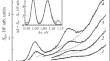
Electric-Field Behavior of the Resonance Features of the Tunneling Photocurrent Component in InAs(QD)/GaAs Heterostructures M. L. OrlovN. S. VolkovaL. K. Orlov SEMICONDUCTOR STRUCTURES, LOW-DIMENSIONAL SYSTEMS, AND QUANTUM PHENOMENA 22 August 2018 Pages: 1129 - 1136
Size-Dependent Optical Properties of Colloidal CdS Quantum Dots Passivated by Thioglycolic Acid T. S. KondratenkoM. S. SmirnovY. A. Vinokur SEMICONDUCTOR STRUCTURES, LOW-DIMENSIONAL SYSTEMS, AND QUANTUM PHENOMENA 22 August 2018 Pages: 1137 - 1144
Quantization of the Electromagnetic Field in Three-Dimensional Photonic Structures on the Basis of the Scattering Matrix Formalism (S Quantization) K. A. IvanovA. R. GubaydullinM. A. Kaliteevski SEMICONDUCTOR STRUCTURES, LOW-DIMENSIONAL SYSTEMS, AND QUANTUM PHENOMENA 22 August 2018 Pages: 1145 - 1149
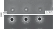
Study of the Structural and Emission Properties of Ge(Si) Quantum Dots Ordered on the Si(001) Surface Zh. V. SmaginaV. A. ZinovyevA. V. Dvurechenskii SEMICONDUCTOR STRUCTURES, LOW-DIMENSIONAL SYSTEMS, AND QUANTUM PHENOMENA 22 August 2018 Pages: 1150 - 1155
On the Impact of Barrier-Layer Doping on the Photoluminescence Efficiency of InGaAlAs/InGaAs/InP Strained-Layer Heterostructures E. S. KolodeznyiA. S. KurochkinD. V. Denisov SEMICONDUCTOR STRUCTURES, LOW-DIMENSIONAL SYSTEMS, AND QUANTUM PHENOMENA 22 August 2018 Pages: 1156 - 1159
Low-Frequency Dielectric Relaxation in Iron-Doped Ge28.5Pb15S56.5 Glassy System R. A. CastroG. I. GrabkoA. A. Kononov AMORPHOUS, VITREOUS, AND ORGANIC SEMICONDUCTORS 22 August 2018 Pages: 1160 - 1162
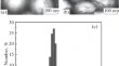
Effect of Conditions of Electrochemical Etching on the Morphological, Structural, and Optical Properties of Porous Gallium Arsenide P. V. SeredinA. S. LenshinA. V. Zhabotinsky MICROCRYSTALLINE, NANOCRYSTALLINE, POROUS, AND COMPOSITE SEMICONDUCTORS 22 August 2018 Pages: 1163 - 1170
Electrical Properties and Energy Parameters of n-FeS2/p-Cd1 –xZnxTe Heterojunctions I. G. OrletskyiM. I. IlashchukS. V. Nichyi MICROCRYSTALLINE, NANOCRYSTALLINE, POROUS, AND COMPOSITE SEMICONDUCTORS 22 August 2018 Pages: 1171 - 1177
On the Formation of IR-Light-Emitting Ge Nanocrystals in Ge:SiO2 Films V. A. VolodinZhang RuiM. Vergnat MICROCRYSTALLINE, NANOCRYSTALLINE, POROUS, AND COMPOSITE SEMICONDUCTORS 22 August 2018 Pages: 1178 - 1187
Effect of Injection Depletion in p-Si–n-(Si2)1 –x(ZnSe)x (0 ≤ x ≤ 0.01) Heterostructure A. S. SaidovA. Yu. LeydermanK. A. Amonov MICROCRYSTALLINE, NANOCRYSTALLINE, POROUS, AND COMPOSITE SEMICONDUCTORS 22 August 2018 Pages: 1188 - 1192
Transport and Photosensitivity in Structures: A Composite Layer of Silicon and Gold Nanoparticles on p-Si M. P. TeplyakovO. S. KenO. M. Sreseli MICROCRYSTALLINE, NANOCRYSTALLINE, POROUS, AND COMPOSITE SEMICONDUCTORS 22 August 2018 Pages: 1193 - 1197
Intercalation of C60 Fullerene Molecules under Single-Layer Graphene on Molybdenum Carbide E. V. Rut’kovN. R. Gall CARBON SYSTEMS 22 August 2018 Pages: 1198 - 1202
Backward-Diode Heterostructure Based on a Zinc-Oxide Nanoarray Formed by Pulsed Electrodeposition and a Cooper-Iodide Film Grown by the SILAR Method N. P. KlochkoV. R. KopachM. G. Khrypunov PHYSICS OF SEMICONDUCTOR DEVICES 22 August 2018 Pages: 1203 - 1214
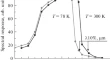
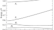
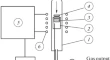
GaSb/GaAlAsSb Heterostructure Photodiodes for the Near-IR Spectral Range E. V. KunitsynaI. A. AndreevYu. P. Yakovlev PHYSICS OF SEMICONDUCTOR DEVICES 22 August 2018 Pages: 1215 - 1220
Lowering the Lasing Threshold by Doping in Mid-Infrared Lasers Based on HgCdTe with HgTe Quantum Wells A. A. DubinovV. Ya. AleshkinS. V. Morozov PHYSICS OF SEMICONDUCTOR DEVICES 22 August 2018 Pages: 1221 - 1224
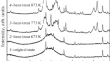
Raman Spectra of Thick Epitaxial GaN Layers Formed on SiC by the Sublimation Sandwich Method A. N. AnisimovA. A. WolfsonE. N. Mokhov FABRICATION, TREATMENT, AND TESTING OF MATERIALS AND STRUCTURES 22 August 2018 Pages: 1225 - 1227