
Abstract
The fabrication of microchannels using MEMS technology always attracted the attention of researchers and designers of microfluidic systems. Our group focused on realizing buried fluidic channels in silicon substrates involving deep reactive ion etching. To meet the demands of today’s complex microsystems, our aim was to create passive microfluidics in the bulk Si substrate well below the surface, while retaining planarity of the wafer. Therefore additional lithographic steps for e.g. integrating circuit elements are still possible on the chip surface. In this paper, a more economic process flow is applied which also contains a selective edge-masking method in order to eliminate under-etching phenomenon at the top of the trenches to be filled. The effect of Al protection on the subsequent etch steps is also discussed. Applying the proposed protection method, our group successfully fabricated sealed microchannels with excellent surface planarity above the filled trenches. Due to the concept, the integration of the technology in hollow silicon microprobes fabrication is now available.
1 Introduction
Bulk micromachined fluidic channels in silicon substrate can act as a fundamental component of local drug delivery systems in neural multi-electrodes. In the last decade a range of fabrication techniques in several structural material has been demonstrated in order to realize hollow microprobes. Standard micromachining tools involve anisotropic wet etching (Chen et al. 1997; Cheung et al. 2003), dry etching techniques (de Boer et al. 2000; Dijkstra et al. 2007), bonding of silicon and glass substrates (Seidl et al. 2010; Sparks and Hubbard 2004) or forming polymer-based hetero-structures (Fernandez et al. 2009; Park et al. 2008; Ziegler et al. 2006).
The use of anisotropic wet etching is quite limited for simple channel networks, since the crystallographic orientation of probes or needles necessarily defines channel shape. This implies that the etchant restricts the preferable orientation of the shaft for the optimal mechanical stability. Combination of anisotropic and isotropic dry etching has shown some promising results, but there is still enough room for further improvements (detailed later).
Besides the leak-free property of wafer bonding, silicon/glass hetero-structures offer only poor exploitation of substrate volume (Sparks and Hubbard 2004). Multilayer SU-8 photoresist (Fernandez et al. 2009), molded poly-dimethyl-siloxane (PDMS) (Park et al. 2008) or parylene (Ziegler et al. 2006) substrates have been utilized in microfluidics as well.
Due to the concept of buried channel technology (de Boer et al. 2000) using highly anisotropic dry etching techniques, several applications has been proposed in the literature (Agarwal et al. 2008; Dijkstra et al. 2007; Paik et al. 2004; Rusu et al. 2001), however, attempt to optimize the original process flow has not been made.
Our group presents an optimized fabrication process of the original channel formation concept, which eventually results in superb surface planarity above the sealed microchannel. The proposed technology is suitable for being integrated into hollow silicon microprobe containing electrodes of small feature size.
2 Objectives
The advantage of BCT is that a network of sealed microchannels can be formed at different depths in bulk silicon. A summary of the currently known and applied technology can be found in a previous paper (de Boer et al. 2000) and also presented in Table 1. The process starts with a DRIE step of a narrow trench. After the trench wall is protected by SiO2 or SiNx deposition, the protective layer at the bottom of the trench is removed by a RIE process to allow the formation of the channel by either anisotropic or isotropic wet or dry etching step.
Major properties considered for improvements or simplifications are as follows:
-
All alternative process flows demonstrated used thermal SiO2 (or LPCVD SiNx) + Cr double layer as a mask in the first step.
-
All of the process flows required protection of the coating layer using a combination of an additional pre-etch step and a sacrificial layer etch, which also limits surface planarity above the microchannels.
-
In all cases costly cryogenic ICP-SF6 plasma etching was used for the Si DRIE of the trench.
-
SiO2, SiNx etch were performed by a RIE, which resulted in greater mask erosion.
3 Channel formation
In Table 1 our simplified process flow is compared to the traditional BCT technology. Several steps of Table 1 (a combination of Cryogenic DRIE and isotropic dry RIE-SF6 recipe), have been enhanced by our group. Detailed process parameters of the applied etch recipes are shown in Table 2.
In this work, all the etching step (including both SiO2 and Si etch) was performed in an Oxford Plasmalab System 100 ICP 3,000 type DRIE.
Initial substrate is a (100) single-crystalline silicon wafer. It should be noticed that the crystallographic orientation and resistivity of the silicon substrate are not critical (step 1). As a masking material for Si etching, thermally grown wet oxide and SPR220 photoresist are used. Since an ICP process is applied for pattern transfer, no additional Cr layer is necessary (step 2). Pattern transfer is completed by a dry etch of SiO2 masking layer in C4F8 + O2 plasma was used for pattern transfer (step 3). In our optimized process no under-etching or sacrificial layer etch is needed, in contrast with Step 3 of the traditional BCT process. In the next step a room temperature Bosch-process is used for deep trench etching (step 4), which is more robust and cheaper than the cryogenic DRIE of the traditional BCT. Aspect ratio better than 1:25 can be now achieved using the Bosch-process (Abdolvand and Ayazia 2008). The surface roughness of the walls, originating from the sequential passivation/etch steps, is approximately 150 nm. As Fig. 1. presents, this roughness causes no problems in the following etching steps. After preliminary trench etch a 100 nm thick thermal SiO2 is grown on the substrate (step 5), which also removes the residual fluorocarbon-polymers from the passivation step of sidewalls during Bosch-process. Electron beam evaporation of a 100 nm thick Al layer follows the oxidation (step 6), which will act as a protective coating not only for the planar surfaces, but also for the trench edge and the rough sidewall as well (Fig. 2). The beneficial effects of the Al layer are detailed in Sect. 5. In order to remove the SiO2 protection layer from the bottom of the trench, an anisotropic etch recipe using CHF3 + Ar plasma chemistry is utilized (step 7). The formation of microchannels (isotropic Si etch) is carried out in SF6 plasma (step 8). During the isotropic Si etch step, the thermally grown 100 nm oxide becomes partially free standing, but still mechanically stable. No bending of the material occurred, which could otherwise close the trench and reduce the etch rate. Wet etching of the sidewall protection in BHF for 10 min removes both Al and SiO2 protection layers (step 9). Figure 1 shows a cross-sectional image of the channel before filling. After dehydration of the wafers at 300°C, an LPCVD process is applied for closing and sealing of the trenches by poly-Si deposition (step 10). An additional annealing of the poly-Si layer at 1,000°C reduces the stress in the deposited layer. A cross section SEM image of a sealed channel is shown on Fig. 3.

Open channels after the isotropic etch of Si

Aluminum step-coverage in the close vicinity of the trench opening

Cross-section of a buried microchannel after the sealing by LPCVD poly-Si deposition is completed
4 Mask protection
The 100 nm thick aluminum masking layer was deposited in order to protect the edges of the trench during both the anisotropic dry SiO2 etching and the isotropic Si etching steps. Since the step-coverage of electron beam evaporation is poor in case of trenches with a small feature size, the bottom of such structures (width close to the micron range) is left almost uncovered, so anisotropic dry oxide etching is not affected significantly (patent pending).
The analysis of the step coverage of the evaporation process was carried out using the planetary evaporation model of SILVACO virtual wafer fab. Model parameters were adjusted according to the experimental setup of the Varian 3,120 vacuum chamber. Al coverage versus aspect ratio at various trench width was simulated by the Elite module and is presented by Fig. 4.

The thickness of Al layer deposited at the bottom of the trench strongly depends on the width (w) and the aspect ratio of that—Al thickness on the plane wafer surface and at the bottom of the trench is denoted by d0 (100 nm) and db, respectively
Images on the step-coverage in the close vicinity of the trench edges are shown on Fig. 2.
The Al passivation of the trench edges also modifies the characteristics of the subsequent etching steps. Different masking layers in DRIE processes can influence not only the etch profile but the etch rate too (Jansen et al. 1996, 2009) Al can easily heat up due to eddy currents, so local rising of temperature might cause increasing etch rate as well as directional changes.
The aspect ratio of the trenches also influences the etch rate. If the aspect ratio is increasing, a thinner Al layer will be present at the bottom of the trench, which affects the anisotropic oxide etch cycle significantly. On the other hand, due to the physical ion depletion and bowing, the effect of diffusion on the supply of reactants to the bottom of the trench, and consumption of reactants at the trench sidewalls is limited (Jansen et al. 1996, 1997), therefore smaller openings are etched slower. These two phenomena are supposed to result in a compensation of aspect ratio dependent etching during the isotropic Si etch (channel formation). The above statements are still being thoroughly investigated in order to determine safety margins of the proposed technology.
5 Results
The final microstructure after isotropic Si etch of the sample is shown on Fig. 3. Some unique features of the proposed method of edge passivation can be concluded as follows:
-
Due to the step-coverage of e-beam evaporation, trenches, channels or reservoirs of larger feature size (aspect ratio <5) on the wafer are substantially protected by the aluminum layer from being etched during isotropic Si etch in SF6 plasma (step 8). The effect is apparent on Fig. 5. That property enables to form the fluidic inlets simultaneously with the channels using the same lithography step.
Fig. 5 
Profile of the isotropic Si etch of a fluidic reservoir (the Si etch is practically inhibited on the surfaces covered by the evaporated aluminum layer)
-
Further advantage of the proposed edge-protection method is that wafers can be exposed to long Si and SiO2 etch cycles due to the high selectivity of both the anisotropic dry oxide etch and the isotropic dry Si etching (Ganji and Majlis 2006) to the Al + SiO2 masking double-layer. As a result, the formation of microchannels buried deeply below the surface (aspect ratio >25) of the silicon substrate is possible.
-
The most apparent benefit of the modified technology is not only the optimized process flow, but the protection of the surface planarity. While under-etching has practically disappeared from the vicinity of the edges, the poor quality of the surface topography above the filled trenches is reduced as well below the micron range (see Fig. 6). Average depth of the orifices is in the 200–300 nm range, while the depth realized by de Boer et al. was approximately 5–10 μm.
Fig. 6 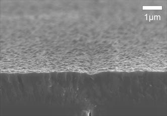
Close SEM view on the surface profile of a sealed trench. It is apparent that the size of the orifice is well below the micron range


Figure 7 shows a cross-sectional view of a fluidic channel fabricated by the new planar process (a), and one realized by the traditional BCT technology, while no protection of the coating layers is performed at all (b). In the third case, the reproducibility and controllability of the process is not reliable. Our enhanced process results in a well-controlled, planar poly-Si surface, which enables the further CMOS processing after buried channel formation is complete.

Sealed microchannels fabricated by the improved technology with mask protection (a), and by the original technology, but without mask protection (b). On the right SEM picture, the collapse of the under-etched masking oxide layers around the trench opening can be clearly seen
6 Conclusion
Our group aimed to make improvements and simplifications in the microfabrication technology of silicon buried microchannels. The edge protection of the trenches before the anisotropic dry oxide etch was achieved by a simple aluminum evaporation step, which finally resulted in excellent surface planarity above the sealed microchannels. In our enhanced process flow, an additional Cr mask is not necessary, and both pre-etch cycles and sacrificial layer etch steps can also be omitted. Moreover, the applied ICP etch recipes results in less damage of the masking layer (Cardinaud et al. 2000). Introducing a room temperature Bosch process instead of cryogenic or mixed mode DRIE the whole process flow becomes more cost-effective.
The sealing properties of the microchannels can be improved further by testing some emerging technology development including tapering (Roxhed et al. 2007) or sidewall smoothness (Gao et al. 2011) of Bosch-process.
The proposed development contributes to the integration of the buried microchannel technology into the fabrication scheme of hollow silicon neural microprobes with high-density electrode system for deep-brain stimulation applications (Schläpfer and Bewernick 2009). Results on the integration are expected to be published in the near future.
References
Abdolvand R, Ayazia F (2008) An advanced reactive ion etching process for very high aspect-ratio sub-micron wide trenches in silicon. Sens Actuator A 144:109–116
Agarwal A, Ranganathan N, Ong WL, Tang KC, Yobas L (2008) Self-sealed circular channels for micro-fluidics. Sens Actuator A 142:80–87
Cardinaud C, Peignon M, Tessier P (2000) Plasma etching: principles, mechanisms, application to micro- and nano-technologies. Appl Surf Sci 164:72–83
Chen J, Wise KD, Hetke JF, Bledsoe SC (1997) A multichannel neural probe for selective chemical delivery at the cellular level. IEEE Trans Biomed Eng. 44:760–769
Cheung KC, Djupsund K, Dan Y, Lee PE (2003) Implantable multichannel electrode array based on SOI technology. J Microelectromech Syst 12:179–188
de Boer MJ, Tjerkstra RW, Berenschot JW, Jansen HV, Burger GJ, Gardeniers JGH, Elwenspoek M, van den Berg A (2000) Micromachining of buried micro channels in silicon. J Microelectromech Syst 9:94–103
Dijkstra M, de Boer MJ, Berenschot JW, Lammerink TSJ, Wiegerink RJ, Elwenspoek M (2007) A versatile surface channel concept for microfluidic applications. J Micromech Microeng 17:1971–1977
Fernandez LJ, Altuna A, Tijero M, Gabriel G, Villa R, Rodraguez J, Batlle M, Vilares R, Berganzo J, Blanco FJ (2009) Study of functional viability of SU-8 based microneedles for neural applications. J Micromech Microeng 19:025007
Ganji B A and Majlis B Y (2006) Deep trenches in silicon structure using DRIE method with aluminum as an etching mask. In: IEEE interernational conference on semiconductor electronics pp 41–47
Gao F, Ylinen S, M. Kainlauri M and Kapulainen M (2011) A modified Bosch process for smooth sidewall etching. In: Proceedings of 22nd micromechanics and microsystems technology Europe workshop, Paper A12
Jansen HV, Gardeniers H, de Boer MJ, Elwenspoek M, Fluitman J (1996) A survey on the reactive ion etching of silicon in microtechnology. J Micromech Microeng 6:14–28
Jansen HV, de Boer MJ, Wiegerink R, Tas N, Smulders E, Neagu C, Elwenspoek M (1997) RIE lag in high aspect ratio trench etching of silicon. Microelectron Eng 35:45–50
Jansen HV, de Boer MJ, Unnikrishnan S, Louwerse MC, Elwenspoek M (2009) Black silicon method X. J Micromech Microeng 19:033001
Paik SJ, Byuna S, Lima JM, Park Y, Lee A, Chung S, Changa J, Chuna K, Choa D (2004) In-plane single-crystal-silicon microneedles for minimally invasive microfluid systems. Sens Actuator A 114:276–284
Park S, Jang Y, Kim H C and Chun K (2008) Fabrication of drug delivery system with piezoelectric micropump for neural probe. In: Proceedings of 23rd International Technical Conference on Circuits/Systems, Computers and Communications 2008, Yamaguchi, Japan pp 1149–1152
Roxhed N, Griss P, Stemme G (2007) A method for tapered deep reactive ion etching using a modified Bosch process. J Micromech Microeng 17:1087–1092
Rusu C, van’t Oever R, de Boer MJ, Jansen HV, Berenschot JW, Bennink ML, Kanger JS, de Grooth BG, Elwenspoek M, Greve J, Brugger J, van den Berg A (2001) Direct integration of micromachined pipettes in a flow channel for single DNA molecule study by optical tweezers. J Microelectromech Syst 10:238–245
Schläpfer TE, Bewernick BH (2009) Deep brain stimulation for psychiatric disorders—state of the art. Adv Tech Stand Neurosurg 34:37–57
Seidl K, Spieth S, Herwik S, Steigert J, Zengerle R, Paul O, Ruther P (2010) In-plane silicon probes for simultaneous neural recording and drug delivery. J Micromech Microeng 20:105006
Sparks D, Hubbard T (2004) Micromachined needles and lancets with design adjustable bevel angles. J Micromech Microeng 14:1230–1233
Ziegler D, Suzuki T, Takeuchi S (2006) Fabrication of flexible neural probes with built-in microfluidic channels by thermal bonding of parylene. J Microelectromech Syst 15:1477–1482
Acknowledgments
The authors would like to thank the staff of MEMS Laboratory, MTA-MFA for their precise contribution to this work. This work was partially supported by ENIAC JTI and the National Innovation Office (NIH) via CAJAL4EU project, the Hungarian National Research Fund (OTKA) via NF69262. The János Bolyai fellowship of the Hungarian Academy of Sciences is also gratefully acknowledged.
Author information
Authors and Affiliations
Corresponding author
Rights and permissions
About this article
Cite this article
Fekete, Z., Pongrácz, A., Fürjes, P. et al. Improved process flow for buried channel fabrication in silicon. Microsyst Technol 18, 353–358 (2012). https://doi.org/10.1007/s00542-012-1430-3
Received:
Accepted:
Published:
Issue Date:
DOI: https://doi.org/10.1007/s00542-012-1430-3