
Abstract
OrCAD/PSpice is a general-purpose computer-aided analysis and design software for electronic circuits. It is an excellent piece of software for circuit computer simulation programs. With strong circuit design and simulation capabilities, it can easily achieve DC analysis, AC analysis, transient analysis, noise analysis, sensitivity analysis, Fourier analysis, harmonic distortion analysis, and circuit performance analysis at different temperatures of electronic circuits. To complete the optimization of component parameters of electronic circuits, it provides a wealth of electronic component models, which can achieve the test of various circuit parameters, the folding function, and the construction function of the device library. With the rapid development of OrCAD/PSpice, the operations become more simplified when various functions are implemented, the programming process is less restricted, and the calculation and simulation of circuits are more accurate. On the basis of grasping the circuit principle, the electronic circuit-assisted simulation design software PSpice can be conveniently used to complete the required circuit design analysis and device characteristic analysis. This paper discusses the application of OrCAD/PSpice software in the analysis of electronic circuits.
Access provided by Autonomous University of Puebla. Download conference paper PDF
Keywords
1 Introduction
OrCAD/PSpice software is the latest version of PSpice, launched by OrCAD, a well-known EDA company in the USA, and MicroSim, which developed PSpice software, in 1998. He changed the inconvenience of text input in general circuit simulation software. Designers can use graphical input methods to draw the circuit in the circuit design window intuitively and conveniently and perform various simulation analyses on the circuit. If it does not meet the design requirements, adjust the circuit structure and component parameters at any time and re-analyze the simulation until the design requirements are met [1]. This kind of analysis, design, and simulation of electronic circuits involves a few clicks, which greatly improves the quality and efficiency of electronic circuit designers.
OrCAD/PSpice is a kind of powerful electronic circuit simulation analysis and design software. It can analyze the basic performance of the circuit according to the structure and parameters of a given circuit. It does not require any actual components and can be used for various functions designed in advance. Applications have replaced a large number of instruments. Circuit designers can use these applications to perform various analyses, calculations, and verifications to complete the analysis of special circuits required.
2 OrCAD/PSpice Features
OrCAD is a software package, and the core software for circuit simulation analysis is PSpice A/D. In order to make the simulation work faster, better, and more flexible, OrCAD software package provides five supporting software to match it: There are circuit diagram generation software (Capture), excitation signal editing software (StmEd, Stimulus Editor), model parameter extraction software (ModelEd, ModelEditor), waveform display and analysis module software (Probe), and optimization program software (Optimizer). It makes rCAD/PSpice have all the analysis functions of electronic engineering design. It cannot only complete the analysis of analog and digital circuits, but also the analysis of mixed digital and analog circuits [2]. Its main analysis functions are:
-
(1)
DC characteristic analysis: including static operating point (Bias PointDetail), DC sensitivity (DCSensitivity), DC transmission characteristic (TF, Transfer Function), and DC characteristic sweep (DCSweep) analysis.
-
(2)
AC analysis: including frequency characteristics (ACSweep) and noise characteristics (Noise) analysis.
-
(3)
Transient analysis: including transient response analysis (TransientAnalysis) and Fourier analysis (FourierAnalysis).
-
(4)
Parameter scanning: including Temperature Analysis and Parametric Analysis.
-
(5)
Statistical analysis: including Monte Carlo analysis (MC, MonteCarlo) and worst-case analysis (WC, Worst Case).
-
(6)
Logic simulation: including logic simulation (Digital Simulation), mixed A/DSimulation, and worst-case timing analysis.
3 The Advantages of OrCAD/PSpice in the Analysis of Electronic Circuits
Oscillation circuits, amplitude modulation circuits, frequency mixing circuits, frequency modulation circuits, and demodulation circuits in electronic circuits are widely used in life. In the design and production, OrCAD/PSpice is used to assist in analyzing the functions and characteristics of the required circuits. The index can easily realize various design needs of electronic circuits. And the application of OrCAD/layout plus can quickly complete the design of actual printed circuit boards that meet the requirements of line performance [3]. The most important thing is that OrCAD/PSpice software calculates accurately, so that the design simulation index is more in line with the actual effect of the circuit. The complexity of electronic circuit design and the high efficiency of OrCAD circuit software make OrCAD/PSpice more fully reflect the advantages of OrCAD-assisted design technology when electronic circuit design, simulation, chopping, and manufacturing: shorten the design cycle and improve the design. The overall efficiency of the manufacturing project has saved design costs; the sensitivity analysis, tolerance analysis, noise analysis, worst-case analysis, and optimized parameter analysis functions in OrCAD have been used to improve and guarantee quality; OrCAD has a large number of unit designs and rich component models and easy-to-adjust model parameters provide convenience for complex design analysis [4]. Although OrCAD provides an efficient platform, when designing and analyzing integrated circuits, you must learn to master OrCAD’s analysis, debugging, and circuit optimization methods so that the performance of OrCAD can be better reflected.
4 Application of OrCAD/PSpice in Electronic Circuit Analysis
4.1 Build the Circuit Schematic
-
(1)
Create a schematic file. On the Windows 10 desktop, execute the command to enter the capture operating environment. Select the menu command and the NewProject dialog box will appear on the screen. In the Name column of this dialog box, the OTL basic amplifier circuit to be analyzed is named al [5].
-
(2)
Load the simulation component library. After completing the new file setting in the NewProject dialog box, click OK to enter the component symbol library setting box; the circuit diagram editing window will appear here [4].
-
(3)
Invoke the simulation component. In the circuit diagram editing window, start the [Place/Part] command. The component symbol selection box appears on the screen. You can select resistance, capacitor, and diode, triode, and excitation graphic symbols and place them in the appropriate position in the circuit diagram. Then select the menu command (Place/Wire) to enable the connection mode to complete the connection and select the menu command (Place/NetAlias) to enable the node setting mode to complete the node setting [6].
-
(4)
Edit component properties. Double-click each component and excitation source icon and select the corresponding name and symbol [7]. The basic OTL complementary symmetrical power amplifier circuit diagram is generated as shown in Fig. 1 (capacitor C3 is open and resistor R2 is short). Design the β = 50 of the triode.
Fig. 1 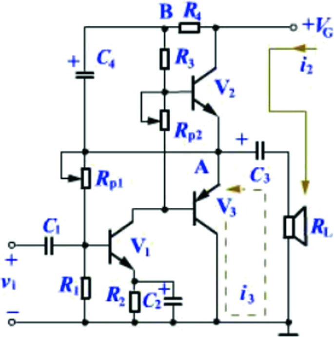
OTL complementary symmetrical power amplifier

4.2 Parameter Setting Analysis
To obtain the maximum undistorted output power, the circuit must have a suitable static operating point [8]. Adjust the bias resistor Rp so that the voltage at the midpoint (point K) of the output stage is equal to 1/2 of the power supply voltage, shown in Fig. 1. That is, Vk = Vom = VCC/2.
-
(1)
The input signal Vi selects a sinusoidal voltage source and sets its amplitude VAMP to 0.
-
(2)
Set Rp as a global variable {Rp, and perform transient analysis and parametric analysis on the circuit at the same time [9]. “Scan variable” is selected as Rp, and the variation range of the variable is 12–16 kΩ with a step size of 0.5 kΩ.
-
(3)
Run PSpice and execute the circuit performance analysis command in the Probe window to get the analysis result shown in Fig. 2. It can be seen that when Rp = 15 kΩ, Vk = VCC/2 = 6.04 V.
Fig. 2 
Relationship between Vk and Rp

4.3 Circuit Analysis and Analysis Results
In an ideal case, the maximum undistorted output voltage amplitude of the circuit is Vom = VCC/2, and the maximum undistorted output power is Pom = (Vom/V2) 2/RL = VCC2/8RL = 0.36 W. Measure the maximum undistorted output power of the circuit in Fig. 3.

Relationship between Vk and V0
-
(1)
The amplitude VAMLP of the input sinusoidal signal Vk is set to the global variable {Vamp}, and transient analysis and parametric analysis are performed at the same time. “Variable” is selected as Vamp. The variation range of the variable is 0–100 mV, and the step size is 20 mV.
-
(2)
Run PSpice, execute the circuit performance analysis command in the Probe window, and obtain the analysis result shown in Fig. 3. It can be seen that when Vo (amplitude) = 3.32 V, it enters the nonlinear region, that is, Vom = 3.32 V, and Pom is obtained Vom2/2RL = 0.11 W.
4.4 Measure the Maximum Undistorted Output Power of the Bootstrap Circuit
The circuit is changed to a bootstrap circuit (connecting capacitor C3 and resistor R2) as shown in Fig. 4. Repeat the steps in 4.3 to get the analysis result shown in Fig. 4, which can be seen at Vo (amplitude) = 5.73. When V, enter the nonlinear region, that is, Vom = 5.73 V, and Pom = 0.33 W.

Relation curve between bootstrap circuit Vk and V0
It can be seen that when V0 (amplitude) is 5.73 V, it enters the nonlinear region, that is, Vom 5.73 V, and Pom = 0.33 V. It can be seen from the above simulation analysis that the bootstrap circuit is closer to an ideal power amplifier [10].
Because there is more capacitor C3 and resistor R2 in the bootstrap circuit, when the product of R2C3 is sufficiently large, the principle that the voltage across the capacitor cannot be abruptly changed, and when the potential at point K approaches VCC, the potential at point a will also increase [11]. So as to ensure that the Q2 tube has sufficient base current, so that the maximum output voltage amplitude Vom approaches VCC/2.
5 Summary
This paper analyzes the circuit based on OrCAD/PSpice’s parameter scan analysis and optimization analysis, which cannot only improve the analysis efficiency, but also make the circuit analysis more optimized, more reliable, and more accurate, especially when the circuit to be optimized is different from its basic function when it is very big. The advantages of using this method for circuit analysis are even more obvious. This method is of great practical value in the analysis of electronic circuits.
References
Jia, XZh. 2018. OrCAD/PSpice practice in the teaching of analog electronic technology. Microelectronics and Computers 8: 32–34.
Zhao, Y.X. 2009. Analysis and design of electronic circuit PSPICE. Journal of Xidian University 3: 121–124.
Wang, FCh. 2016. Design of signal generation circuit based on OrCAD/PSpice. Microelectronics and Computer 11: 55–57.
Kang, H.G. 2010. Design of signal generation circuit based on OrCAD/PSpice. Journal of Xidian University 7: 77–79.
Duan, XCh., and T.X. Zhao. 2015. IC optimized design and yield forecast. Microelectronics and Computer 4: 67–71.
Li, Y.P., and X.T. Wu. 2014. Design of signal generation circuit based on OrCAD/PSpice. Microelectronics and Computer 12: 88–91.
Zheng, ChF, and Y.H. Ma. 2005. Research and application of circuit optimization design algorithm based on EDA. Microelectronics and Computer 5: 139–141.
Jia, X.Z., and Y.F. Hao. 2017. Application of OrCAD/pspice9 circuit design. Journal of Xidian University 9: 64–67.
Pan, Y.C., and W.X. Wang. 2017. OrCAD/pspice-based circuit optimization design. Semiconductor Technology 9: 28–31.
Zeng, Z.H., X.Z. Jia, and N.T. Liu. 2013. Electronic circuit design based on OrCAD/pspice platform. Journal of Xidian University 1: 66–69.
Wang, D.F., and J.J. Lu. 2018. OrCAD circuit design software based high frequency electronic circuit simulation analysis. Semiconductor Technology 11: 17–19.
Acknowledgements
Fund Project: This paper is the outcome of the study, Research on Blended Learning under the Background of Internet +, which is supported by the Foundation for Projects of the Education Management Information Center of the Ministry of Education in 2017. The Project Number is EIJYB2017-073.
Author information
Authors and Affiliations
Corresponding author
Editor information
Editors and Affiliations
Rights and permissions
Copyright information
© 2020 Springer Nature Singapore Pte Ltd.
About this paper

Cite this paper
Chi, H. (2020). The Application of OrCAD/PSpice Software in Electronic Circuit Analysis. In: Yang, CT., Pei, Y., Chang, JW. (eds) Innovative Computing. Lecture Notes in Electrical Engineering, vol 675. Springer, Singapore. https://doi.org/10.1007/978-981-15-5959-4_215
Download citation
DOI: https://doi.org/10.1007/978-981-15-5959-4_215
Published:
Publisher Name: Springer, Singapore
Print ISBN: 978-981-15-5958-7
Online ISBN: 978-981-15-5959-4
eBook Packages: Computer ScienceComputer Science (R0)