
Abstract
Encryption technology that based on quantum circuit is an important technology in the field of information security and the encryption system designed by this technology can improve the encryption effect, and its anti-attack ability is (\( 2^{\text{n}} \) − 1)! times of the traditional method. In order to increase the complexity of the key that belongs to the encryption system, we propose a method of constructing the algorithm of key extension based on quantum circuit and finish the design of the key extension module, in the method, we transform the nonlinear transformation into linear transformation which can be constructed by quantum circuit easily, and complete the transformation of operation in quantum logic which can simplify the generation process while maintaining the same performance. In order to increase the practicability of encryption system based on quantum circuit, we analyze the characteristics of the encryption system and complete the design of the interface module. What’s more, the key extension module and the interface module are tested under the environment of QUARTUS and real object, and the validity and correctness of the two modules are verified.
Access provided by Autonomous University of Puebla. Download conference paper PDF
Keywords
1 Introduction
With the booming of new information technologies such as cloud computing and IOT, all kinds of data are expanding rapidly [1]. However, most kinds of emerging technologies are still in the initial stage of development with the immature information protection technology, so there will inevitably be security problems such as Information theft, tampering and disclosure when a large number of sensitive information is processed, transmitted and stored on the network. Therefore, reliable and efficient technology of encryption has become a research hotspot in all walks of life [2]. Encryption technology that based on quantum circuit is an important technology to protect the security of network. It uses quantum circuit to construct encryption algorithm and realizes it with hardware to form encryption system of quantum circuit, the encryption system can not only improve the encryption efficiency, but also increase the encryption complexity by (\( 2^{\text{n}} \) − 1)! times [3].
Document [3] proposes a construction method of quantum circuit for multiplication in finite field, and constructs encryption algorithm based on the method, however, it only completes the hardware design of the encrypted part and the decrypted part based on quantum circuit. In reference [4], a quantum circuit implementation method is proposed for S-box transformation in AES algorithm, and the idea of constructing encryption algorithm based on quantum circuit is proposed. Literature [5] proposes Quantum fully homomorphic encryption scheme based on universal quantum circuit and does research on the process of quantum information. In reference [6], authors describe the advantages and feasibility of applying reversible Logic in cryptography and coding theory on the basis of confirmatory study. Document [7] proposes a method of synthesis and optimization for linear nearest neighbor quantum circuits by parallel processing which can reduce the quantum cost for the design and implementation of quantum circuits.
The existing literatures provide a theoretical idea for the research of encryption system based on quantum circuit, and complete the design of encryption and decryption part. However, the encryption and decryption process of the encryption system needs the participation of the key. The complexity and security of the key largely determine the encryption complexity and anti-attack ability of the encryption system, so the design of the key extension and generation part is particularly important. Furthermore, the encryption system must have an interface to interact with users or devices in the practical application, so the design of the interface part is also essential.
For the purpose of improving the complexity of key generation in the encryption system and increasing the security of the key, this paper designed the key extension module based on quantum circuit. And this module can expand the combination types of generated key to \( 2^{\text{n}} ! \), greatly increase the difficulty of cracking. At the same time, in order to improve the practicability of the encryption system, an interface module is designed, and the user or device can implement encryption and decryption operations of information through different interfaces in the module.
2 Relevant Technology
2.1 Quantum Gate
Quantum gates are basic units of quantum circuits], it can be expressed by matrix or vector multiplication which means states of quantum bit [8]. Common quantum gates are CNOT gates and SWAP gates, Fig. 1 shows a CNOT gate, when the control bit B is 1, the target bit A is reversed, and when the control bit B is 0, the target bit A remains unchanged. Figure 2 shows a SWAP gate, which indicates that two connected quantum bits A and B will be exchanged, so it is also called a switching gate.

CNOT gate

SWAP gate
2.2 Quantum Circuit
Quantum circuit is a logic circuit with function and is built by a series of quantum gates [8]. Quantum circuit has \( 2^{\text{n}} ! \) kinds of substitutions for the input of n-bits, its input number is equal to the output number and it has no heat loss, no fan-in, no fan-out, no feedback [5]. Figure 3 is a quantum circuit which consists of seven SWAP gates cascaded with three CNOT gates, it represents the multiply 2 operation on a finite field.

Quantum circuit
2.3 Encryption Technology and Encryption System of Quantum Circuit
Encryption technology of quantum circuit is to apply the characteristics of non-feedback and high complexity of quantum circuitry to the field of encryption technology, it can design encryption algorithms based on quantum circuit [3]. The encryption system of quantum circuit is designed by encryption technology of quantum circuit, it consists of four parts: encryption module, decryption module, key extension module and interface module, Among them, encryption module, decryption module and key extension module are all constructed based on quantum circuit, meanwhile the interface module is designed by hardware language which can adapt to the characteristics of quantum circuits and work with encryption and decryption module.
Figure 4 is the framework of the encryption system. The key extension module and interface module designed in this paper are used to work with the encryption module and the decryption module to improve the performance of them. The key extension module is connected to the encryption and decryption module in order to provide the required keys for them. Similarly, the interface module is connected to the encryption and decryption module, it can supply convenience for users to exchange information with them and realize the operation of information encryption or decryption. In addition, A switch is used in the system to decide whether the information enters the encryption module or the decryption module, and also decide whether the information is output by the encryption module or the decryption module.

Structural framework of encryption system
3 Design of Key Extension Module Based on Quantum Circuit
3.1 Key and Key Extension
In cryptography, the key is secret data used to complete cryptographic applications [9]. In the encryption system designed in this paper, the key is used for the encryption and decryption module to complete the encryption and decryption operations.
Key extension refers to the extension of the initial key with a small number of bits into the key with large number of bits [9]. In the encryption system designed in this paper, the initial key has 128 bits, which needs to be extended to 1408 bits, the extended keys are called round key. The necessities of key extension are as follows:
-
1.
The key extension can eliminate the symmetry and similarity of the generation methods for different keys, and increase the complexity of the key, thus improving the encryption complexity of the encryption system.
-
2.
The key extension can expand the difference of the key, therefore, each bit of the initial key can directly or indirectly affect many bits in the process which will make key cracking more difficult.
-
3.
The key extension makes the key sufficiently non-linear to prevent that the difference of the keys completely determined by the initial key, thus the key extended from the initial key can also affect the other extended keys, and it will expand the difference of many steps in encryption process to enhance the encryption effect.
3.2 Introduction of Key Extension Algorithms
Key extension is the process of expanding 128-bit initial key to 1408-bit round key. For convenience, we regard 128-bit initial key as a matrix with four rows and four columns, each element of the matrix has 8-bit data. The key extension process is as follows:
-
1.
The four elements in a column of matrix is counted as W[j], it has 32 bits, therefore, the initial keys are counted as W[0], W[1], W[2], W[3];
-
2.
The extended keys are also expressed in the form of W[j], where j is an integer and the range of it is [4, 43].
-
3.
If j%4 = 0, w[j] = w[j − 4] ⊕ g(w[j − 1]), otherwise, w[j] = w[j − 4] ⊕ w[j − 1]. Where “g()” represents g-function and “⊕” denotes XOR.
The contents of g-function are as follows:
-
a.
Move the corresponding W[j] cycle to the left by 8 bits;
-
b.
S-box substitution for each byte in the corresponding W[j];
-
c.
XOR the corresponding W[j] with constants (Rcon[j/4], 0, 0, 0), Rcon is a one-dimensional array, Rcon[1] = 0 × 01, Rcon[i] = Rcon[i − 1]*(02) (i > 1, “*(02)” represent multiplication over finite fields).
3.3 Theory of Designing Key Extension Algorithms Based on Quantum Circuits
Feasibility and Necessity
-
1.
The step (b) of g-function in key extension algorithm involves S-box replacement, which maps an 8-bit data to another 8-bit data by searching the S-box table. The traditional way to realize S-box replacement is to store the S-box table in read-only memory, and then compare the input 8-bit data with the memory to find the corresponding 8-bit data. Using quantum circuit to realize S-box replacement does not need the tedious operation of looking up tables, it evolves the logic of S-box table into the conversion relationship between finite field and compound field and the result can be obtained only by conversion between different fields. In the whole process, only addition on the finite field is involved which can be implemented by using simple CNOT gates. Therefore, realizing S-box replacement based on quantum circuits can not only accelerate the replacement rate and reduce the delay time, but also reduce power consumption and hardware size [10].
-
2.
The step (c) of g-function in key extension algorithm involves XOR, division and multiplication over finite fields. Traditional methods for hardware to implement division operation is that they first expand the digits of the dividend, and then continuously compare the high digits of the dividend with the divisor to determine the value of quotient until the end of the calculation. The whole process involves many operations such as comparison, subtraction and shift. If we implement division operations with quantum circuits, it generally involves only shift operation which can be implemented by SWAP gates in quantum circuits. In addition, XOR is equivalent to addition over finite fields. Document [3] designs a method for quantum circuits to implement operations over finite fields, and draws a conclusion that the operation rate is higher. Therefore, the implementation of this step based on quantum circuits can simplify the process, make the operation faster and reduce the delay [11].
-
3.
The key extension algorithm contains many operations. The operations of dividing, XOR and g- function in formulas have been introduced in the preceding article, On the step of controlling the XOR of two data according to the value of “j%4”, the traditional methods will design the data selector, when the quantum circuit realizes it by using the TOFFOLI gates which have double control bits. So the quantum circuit can realize critical path with high working frequency and reduce the occupancy of resources in hardware.
Advantages of Designing Key Extension Algorithm Based on Quantum Circuit.
Designing Key Extension Algorithm based on quantum circuit does not change the algorithm itself and the complexity, what change are the implementation method of the algorithm. Therefore, the characteristics of quantum circuits will be applied to the algorithm, add the following three advantages for the key extension:
-
1.
Quantum circuit’s input number is equal to output number, it has no fan-in, no fan-out, no heat loss [6]. Therefore, using quantum circuit to implement key extension algorithm can greatly reduce the energy consumption in the process of key extension, reduce the occupancy rate of hardware resources, and improve the rate at which the key expands.
-
2.
There are \( 2^{\text{n}} ! \) kinds of reversible networks for input and output vectors of quantum circuits, and there are \( 2^{\text{n}} ! \) kinds of permutations for input of n-bit data [6]. Therefore, the implementation of key extension algorithm with quantum circuit can increase the complexity of the key extension process by (\( 2^{\text{n}} \) − 1)! times and it is difficult to get all the secret keys from the partially extended keys, as a result, it greatly increases the security of key extension.
-
3.
In the encryption system, the key extension module is connected with the encryption and decryption module to work with them, the encryption and decryption module are constructed by quantum circuits, Therefore, implementing the key extension algorithm based on quantum circuits can make the key extension module combine with encryption and decryption module more closely, and improve the ability of the whole cooperative work.
3.4 Implementation of Key Extension Algorithms Based on Quantum Circuit
The implementation of the key extension module is mainly divided into two steps, Firstly, we complete the design of g-function, and then complete the implementation of key extension according to the formula.
Realization of g-Function
-
1.
Left shift of circulation. Left shift of circulation is to move the W[j] to the left for 8 bits. Since the operation of left shift is only a change of bit’s position, the quantum circuit can be constructed by using the quantum SWAP gate, when converting it to hardware circuit we can change the output sequence of circuit layout.
-
2.
S-box replacement. S-box replacement is to replace the four bytes in W[j] with another four bytes. In the implementation, the data W[j] in the finite domain \( {\text{GF}}(2^{8} ) \) is transformed into its composite domain \( {\text{GF}}\left( {(2^{4} )^{2} } \right) \), after inversion in the composite domain, the data is transformed back into the finite domain [10], finally the reversible affine transformation is carried out and S-box replacement is finished.
-
3.
XOR of Rcon. XOR of Rcon is an operation that realize XOR of W[j] and 32-bit constant (Rcon[j/4], 0, 0, 0). Since the (Rcon[j/4], 0, 0, 0) is all zero except Rcon, the first step is to construct the circuit to generate the values of Rcon. In addition, using different values in Rcon array for XOR is depending on the value of “j/4”, so it is necessary to construct the circuit to generate the value of “j/4”.
-
(1)
Circuit Construction of Generating Rcon Values. Rcon is a one-dimensional array, Rcon[1] = 0 × 01, Rcon[i] = Rcon[i − 1]*(02) (i > 1, “*(02)” is the multiplication over finite fields). Since 128-bit seed keys are expressed as W[0] to W [3], the extended secret keys are expressed as W[4] to W[43], therefore the range of “j” in W[j] is [4, 43], and the range of “j/4” is [1, 10], Rcon array only needs to calculate the values of Rcon[1] to Rcon[10]. The quantum circuits of generating Rcon value are shown in Fig. 5. It is necessary to prepare quantum bits with initial state of | 00000001> to initialize the value of Rcon[1], then we use SWAP gate and CNOT gate to realize multiplication of 2 over finite fields, the circuit of multiplication is encapsulated as U device, and after Cascading 9 U devices with 8 CNOT gates [3], the construction of quantum circuit is finished. When Converting it into hardware circuit, we represent quantum auxiliary bit | 1 > with high levels, and quantum auxiliary bits | 0 > with low levels, then cascade them with nine U devices to build hardware circuit. The hardware circuit in Quartus environment is shown in Fig. 6.
Fig. 5. 
Quantum circuit graph of value generation of the Rcon array
Fig. 6. 
Hardware circuit graph of value generation of the Rcon array
-
(2)
Circuit Construction of “j/4” Operation. “j/4” means that j is divided by 4 to take an integer. The operation of dividing 8-bits data by 4 can be obtained by shifting the data to the right by two bits, Suppose that the value of “j” is \( {\text{b}}_{7} {\text{b}}_{6} {\text{b}}_{5} {\text{b}}_{4} {\text{b}}_{3} {\text{b}}_{2} {\text{b}}_{1} {\text{b}}_{0} \), then the two digits (\( {\text{b}}_{1} {\text{b}}_{0} \)) removed from the low bits are the remainder, and the value (\( 00{\text{b}}_{7} {\text{b}}_{6} {\text{b}}_{5} {\text{b}}_{4} {\text{b}}_{3} {\text{b}}_{2} \)) is the integral value divided by four. When constructing the operation of “j/4” based on quantum circuits, we use auxiliary bits | 0 > to supplement the two high bits [3] the right-shift operation can be implemented by SWAP gates. When converting quantum circuits into hardware circuits, we represent quantum bit |1 > with high level, and quantum bit | 0 > with low level, the shift operation requires changing position during layout. Quantum circuit of dividing four operations designed in this paper is shown in Fig. 7.
Fig. 7. 
Quantum circuit graph of the operation of dividing 4
-
(1)
-
4.
Encapsulation of g-Function circuit. The construction of key extension based on quantum circuits is complex. In order to introduce the construction of subsequent quantum circuits, we simplify the circuits of g-Function logically, encapsulate the g-Function circuits in three steps 1, 2 and 3 as G devices, as shown in Fig. 8.
Fig. 8. 
G device


Overall Design of Key Extension Algorithms
The core content of key extension algorithm is as follows: If j%4 = 0, w[j] = w[j − 4] ⊕ g(w[j − 1]), otherwise, w[j] = w[j − 4] ⊕ w[j − 1]; Since the whole quantum circuit of key extension is complex and every four lines is a construction cycle, we only shows the partial quantum circuit of the key extension in Fig. 9. In the figure, the left side is the input, the right side is the output, “| 0000… >” represents | 0 > auxiliary bits of 32 bits.

Quantum circuit diagram of key extension module
When implementing the algorithm, XOR can be implemented by CNOT gates, the g-function has been realized before which is represented by a G device. After cascading 80 CNOT gates and 10 G devices according to the rules, we finish the overall design of key extension based on quantum circuit. When converting it to hardware circuit, we can use logical gate XOR to implement CNOT gate. The partial hardware circuit in the Quartus environment is shown in Fig. 10, the left side is the input, the right side is the output, and the “0000…” means 0 bit which length is 32-bit.

Hardware circuit diagram of key extension module
4 The Design of Interface Module
In order to make it easier for users to use the encryption module and the decryption module, we research on the characteristics of the encryption and decryption module and design the interface module to match them. The interface module has multiple types of interface, such as UART, SPI, and the different interfaces can meet different needs of users. The following takes the SPI interface as an example to describe how the interface module is designed.
4.1 Introduction of the SPI Interface
SPI is a high-speed, full-duplex, synchronous communication bus [13] with four IO pins: SCLK, MOSI, MISO, CS. When the SPI data is transmitted, the host selects the slave to communicate according to “CS”, and then sends data according to the clock “SCLK” via the “MOSI” line, the slave reads the data through the line. After that the slave sends data from the MISO line, and the host reads data from the same line [13], this process loops until the data transfer is complete. In addition, the SPI interface needs to set the phase and polarity, the polarity (CPOL) sets the level of the idle clock and the phase (CPHA) sets the clock edge for transmission of data. The phase and polarity of the master and slave must be the same.
4.2 The Design of SPI Interface
The encryption and decryption module perform operations on the data sent by the user, so the encryption and decryption module is a slave device, and the interface designed in this paper is an interface of the slave device. Since the encryption and decryption module perform operations on every 128 bits of data, a cache is needed to temporarily store data received and to be transmitted from the device. We set the phase and polarity to zero, in addition, when the operations of encryption and decryption are finished, the processed information needs to be output, so the interface module is divided into an input interface module and an output interface module. This article uses the Verilog language to implement the design of the SPI interface.
Input Interface Module.
The users or devices can input data into the encryption or decryption module through the input interface module. Figure 11 is a logical representation of the SPI input interface in the Quartus environment, in the figure, “SPI_in_8” implements the function of receiving one byte of data and it stores the 8-bit data received each time into the buffer “Buffer_128”. When the buffer is full of 128-bit data, the 128-bit data is output to the corresponding encryption module or decryption module. The main implementation steps are as follows:
-
1.
Capture the Trigger Edge. Each step of the SPI must be performed after the trigger edge of the clock is generated and this article sets the rising edge as the trigger edge. “sck_r1” is used to record the high or low of the previous clock, and “sck_r0” is used to record the high or low of the next clock. If “sck_r1” is low and “sck_r0” is high, the rising edge is captured.
-
2.
Receive and Store 8-bit Data. The first step is to determine whether the user wants to send data for encryption and decryption, this step can be achieved by determining whether the selection signal is low level. If the selection signal is low, the value obtained by the pin “MOSI” will be stored in the register under the clock. When the rising edge is captured and the select signal is 0, the data will be received. Meanwhile, the number of the received data is recorded and when the number is full of 8 bits, the value of corresponding flag is set to 1 and it indicates the completion of data transmission in one byte.
-
3.
Setting 128-bit buffer. The data of the register in step 2 will be input into the buffer, and when the buffer is stored in 128-bit data, the data will be output to the encryption module or the decryption module. In implementation, we can define memory data which is 16 bits long and 8 bits wide to store 8-bit data received at a time. In addition, a switch is needed to determine whether the data in buffer enter the encryption module or decryption module.
-
4.
Data Filling. When the number of bits needed to be encrypted is not a multiple of 128, it is necessary to fill in the data to meet the requirements of data size in buffer. We record the number of bytes entering the buffer, if the number less than 16, all the bytes in the vacancy are set at 0-bit. When the data is restored, the original data can be obtained only by clearing all the parts that is set to 0-bit.

Logic diagram of input interface module
Output Interface Module.
The data processed by encryption or decryption module is output by output interface module. The output interface module and the input interface module are inverse processes and their implementation methods are similar, therefore, this article does not make a superfluous introduction for it.
5 Verification and Testing
In order to verify the validity of the key extension module and the interface module, we verify the key generation of the key extension module and carry out the transmission test of the interface module. Then the analysis results are obtained.
5.1 Verification of the Key Extension Module
The key extension module expands the original key of 128-bit into the key of 1408-bit according to the rule, each 32-bit key is a group and there are 44 groups in total. The process of verification is as follows:
-
1.
The 128-bit original key (hexadecimal) entered is “ 3E 19 3D 71 25 56 6A 49 4F 4B 3F 7C 2A 8C 62 23”.
-
2.
The 1408-bit extended key (hexadecimal) generated is shown in Table 1.
Table 1. 1408-bit Extended key
The above keys are shown in hexadecimal form, every two characters represents hexadecimal number of 8-bit. The extended keys in Table 1 represent a set of 32-bit keys from top to bottom, the first list shows W[0] to W[21], the second list shows W[22] to W[43]. The number of output key is 1408 bits, and the content of them conforms to the logic of the key extension algorithm, therefore Verification passed.
5.2 Transfer Test of Interface Module
Taking SPI interface as an example, this paper builds a communication environment including master device and slave device to verify the correctness of the interface.
Test Preparation.
-
1.
SPI Upper Computer. The upper computer is the host equipment, which is used to communicate with the slave interface designed in this paper. The right of Fig. 12 shows a USB-to-SPI device, Users can set the length of transmission data and see the data sent and received through the corresponding software.
Fig. 12. 
Physical connection diagram of upper and lower machine
-
2.
SPI Lower computer. The SPI lower computer is a slave device, which can communicate with the upper computer. Firstly, we connect the two output pins of the input module directly with the corresponding input pins of the output module, so that the information received by the input module will be directly transmitted to the output module for output, which is convenient for testing. Secondly, the connected lines are burned into the core board of the FPGA which is shown in the left of Fig. 12, and after setting the pin parameters, the FPGA has the function of SPI interface designed in this paper [14], which is used as the lower computer.
-
3.
Connection of Upper and Lower Computer. Connecting the prepared upper computer with the lower computer in the way shown in Fig. 12 when the upper computer connects the PC.

Testing Process
-
1.
Input the data to be transmitted. As shown in Fig. 13, we input hexadecimal data of 8-bit in each address, totaling 16 addresses, so the total length is 128 bits.
Fig. 13. 
Input data
-
2.
Receive the data returned by the lower computer. The data read by the host computer from MISO is shown in Fig. 14.
Fig. 14. 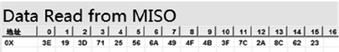
Received data


As can be seen from the above two graphs, the data transmitted from the host computer to the FPGA is exactly the same as the data received from the FPGA, and the verification is successful.
6 Summary
This paper designs and implements the key extension module based on quantum circuit and interface module based on logic language, it also verify the correctness and validity of the two modules. This design can be used in the encryption system of quantum circuit to improve the encryption complexity, cracking difficulty and practicability. In the further work, we will design the two modules into the encryption system even better, and construct a complete encryption system to protect the hot technologies in urgent need of security, such as narrowband Internet of Things.
References
Xu, L., Jiang, C., Wang, J.: Information security in big data: privacy and data mining. IEEE Access 2, 1149–1176 (2014)
Natalia, M., Alexander, T.: Internet of Things: information security challenges and solutions. Cluster Comput. 22, 103–106 (2018)
Chen, J., Guan, Z., Chen, X.: Design and hardware implementation of quantum reversible logic encryption algorithms. J. PLA Univ. Sci. Technol. (Nat. Sci. Ed.) 0(0), 1–3 (2018)
Liu, Y., Zhu, F.: Quantum circuit implementation of S-Box transform in AES. Inf. Secur. Commun. Secrecy 5, 92–94 (2008)
Liang, M.: Quantum fully homomorphic encryption scheme based on universal quantum circuit. Quantum Inf. Process. 14(8), 2749–2754 (2015)
Datta, K., Sengupta, I.: Applications of reversible Logic in cryptography and coding theory. In: International Conference on Vlsi Design and International Conference on Embedded Systems, pp. lxvi–lxvii. IEEE Computer Society. Washington DC (2013)
Zhang, Z., Guan, Z., Zhan, H.: A method of synthesis and optimization for linear nearest neighbor quantum circuits by parallel processing. Quantum Inf. Comput. 18(13), 1095–1114 (2018)
Li, Z., Chen, S., Song, X.: Quantum Circuit synthesis using a new quantum logic gate library of NCV quantum gates. Int. J. Theor. Phys. 56(4), 1023–1038 (2017)
Du, Z., Xu, Q., Zhang, J.: The design of a key extension algorithm based on dynamic dislocation counts. In: 11th International Conference on Computational Intelligence and Security (CIS), pp. 345–349. IEEE, Shenzhen (2015)
Guan, Z., Chen, J., Chen, X.: Implementation method of quantum byte replacement hardware module for AES hardware encryption system: CN108322305A[P], 24 July 2018
Nayak, A., Sen, P.: Invertible Quantum Operations and Perfect Encryption of Quantum States. Quantum Inf. Comput. 7(1–2), 103–110 (2012)
Bossuet, L., Datta, N., Mancillas-Lopez, C.: ELmD: a pipelineable authenticated encryption and its hardware implementation. IEEE Trans. Comput. 65(11), 3318–3329 (2016)
Wei, P., Zhang, C., Huang, X.: Design of a high-performance and dynamic reconfigurable SPI IP core with master and slave mode. Appl. Electron. Tech. 44(3), 15–18 (2018)
Xie, Z.: A design of PCI target interface based on FPGA. Adv. Mat. Res. 186, 342–347 (2011)
Acknowledgements
This work was partially supported by National Natural Science Foundation of China (NO. 61402244), Natural Science Foundation of Jiangsu Province (NO. BK20151274) and Next Generation Project of Technology Innovation for CERNET Internet (NO. NGII20180310).
Author information
Authors and Affiliations
Corresponding author
Editor information
Editors and Affiliations
Rights and permissions
Copyright information
© 2020 Springer Nature Singapore Pte Ltd.
About this paper

Cite this paper
Wang, C., Sun, J., Guan, Z., Chen, J., Li, Y. (2020). Design and Implementation of Key Extension and Interface Module Based on Quantum Circuit. In: Li, K., Li, W., Wang, H., Liu, Y. (eds) Artificial Intelligence Algorithms and Applications. ISICA 2019. Communications in Computer and Information Science, vol 1205. Springer, Singapore. https://doi.org/10.1007/978-981-15-5577-0_6
Download citation
DOI: https://doi.org/10.1007/978-981-15-5577-0_6
Published:
Publisher Name: Springer, Singapore
Print ISBN: 978-981-15-5576-3
Online ISBN: 978-981-15-5577-0
eBook Packages: Computer ScienceComputer Science (R0)