
Abstract
This chapter describes the classical architecture of many digital circuits and presents, by means of several examples, the conventional techniques that digital circuit designers can use to translate an initial algorithmic description to an actual circuit. The main topics are the decomposition of a circuit into Data Path and Control Unit and the solution of two related problems, namely scheduling and resource assignment.
Access provided by Autonomous University of Puebla. Download chapter PDF
Keywords
These keywords were added by machine and not by the authors. This process is experimental and the keywords may be updated as the learning algorithm improves.
This chapter describes the classical architecture of many digital circuits and presents, by means of several examples, the conventional techniques that digital circuit designers can use to translate an initial algorithmic description to an actual circuit. The main topics are the decomposition of a circuit into Data Path and Control Unit and the solution of two related problems, namely scheduling and resource assignment.
In fact, modern Electronic Design Automation tools have the capacity to directly generate circuits from algorithmic descriptions, with performances—latency, cost, consumption—comparable with those obtained using more traditional methods. Those development tools are one of the main topics of Chap. 5. So, it is possible that, in the future, the concepts and methods presented in this chapter will no longer be of interest to circuit designers, allowing them to concentrate on algorithmic innovative aspects rather than on scheduling and resource assignment optimization.
2.1 Introductory Example
As a first example, a “naive” method for computing the square root of a natural x is considered. The following algorithm sequentially computes all the pairs [r, s = (r + 1)2] with r = 0, 1, 2, etc.:

Initially r = 0 and thus s = 1. Then, at each step, the pair [r + 1, (r + 2)2] is computed in function of r and s = (r + 1)2:
The same method can be used for computing the square root of x. For that, the loop execution is controlled by the condition s ≤ x.
Algorithm 2.1: Square root

The loop is executed as long as s ≤ x, that is (r + 1)2 ≤ x. Thus, at the end of the loop execution,
Obviously, this is not a good algorithm as its computation time is proportional to the square root itself, so that for great values of x (x ≅ 2n) the number of steps is of the order of 2n/2. Efficient algorithms are described in Chap. 10.
In order to implement Algorithm 2.1, the list of operations executed at each clock cycle must be defined. In this case, each iteration step includes three operations: evaluation of the condition s ≤ x, s + 2·(r + 1) + 1 and r + 1. They can be executed in parallel. On the other hand, the successive values of r and s must be stored at each step. For that, two registers are used. Their initial values (0 and 1 respectively) are controlled by a common load signal, and their updating at the end of each step by a common ce (clock enable) signal. The circuit is shown in Fig. 2.1.

Square root computation: data path
To complete the circuit, a control unit in charge of generating the load and ce signals must be added. It is a finite state machine with one input greater (detection of the loop execution end) and two outputs, load and ce. A start input and a done output are added in order to allow the communication with other circuits. The finite state machine is shown in Fig. 2.2.

Square root computation: control unit
The circuit of Fig. 2.1 is made up of five blocks whose VHDL models are the following:
-
computation of next_r:

-
computation of next_s:

(multiplying by 2 is the same as shifting one position to the right)
-
register r:

-
register s:

-
end of loop detection:

The control unit is a Mealy finite state machine that can be modeled as follows:
-
next state computation:

-
output state computation:


The circuit of Fig. 2.1 includes three n-bit adders: a half adder for computing next_r, a full adder for computing next_s and another full adder (actually a subtractor) for detecting the condition s > x. Another option is to use one adder and to decompose each iteration step into three clock cycles. For that, Algorithm 2.1 is slightly modified.
Algorithm 2.2: Square root, version 2

A circuit able to execute the three operations, that is r + 1, s + 2·r + 1 and evaluation of the condition s > x must be defined. The condition s > x is equivalent to s ≥ x + 1 or s + 2n − 1 − x ≥ 2n. The binary representation of 2n − 1 − x is obtained by complementing the bits of the binary representation of x. So, the condition s > x is equivalent to s + not(x) ≥ 2n. Thus, the three operations amount to additions: r + 1, s + 2·r + 1 and s + not(x). In the latter case, the output carry defines the value of greater. The corresponding circuit is shown in Fig. 2.3. It is an example of programmable computation resource : under the control of a 2-bit command operation, it can execute the three previously defined operations.

Square root computation: programmable computation resource
The corresponding VHDL description is the following:

The complete circuit is shown in Fig. 2.4.

Square root computation, second version: data path
A control unit must be added. It is a finite state machine with one input greater and five outputs load, ce_r, ce_s, ce_greater. As before, a start input and a done output are added in order to allow the communication with other circuits. The finite state machine is shown in Fig. 2.5.

Square root computation, second version: control unit
The building blocks of the circuit of Fig. 2.4 (apart from the programmable resource) are the following:


2.2 Data Path and Control Unit
The general structure of a digital circuit is shown in Fig. 2.6. It consists of a data path and a control unit. The data path (leftmost part of Fig. 2.6) includes computation resources executing the algorithm operations, registers storing the algorithm variables, and programmable connections (for example multiplexers, not represented in Fig. 2.6) between resource outputs and register inputs, and between register outputs and resource inputs. The control unit (rightmost part of Fig. 2.6) is a finite state machine. It controls the sequence of data path operations by means of a set of control signals (commands) such as clock enables of registers, programming of computation resources and multiplexers, and so on. It receives from the data path some feedback information (conditions) corresponding to the algorithm control statements (loop, if, case).

Structure of a digital circuit: data path and control unit
In fact, the data path could also be considered as being a finite state machine. Its internal states are all the possible register contents, the next-state computation is performed by the computation resources, and the output states are all the possible values of conditions. Nevertheless, the number of internal states is enormous and there is generally no sense in using a finite state machine model for the data path. However, it is interesting to observe that the data path of Fig. 2.6 is a Moore machine (the output state only depends on the internal state) while the control unit could be a Moore or a Mealy machine. An important point is that, when two finite state machines are interconnected, one of them must be a Moore machine in order to avoid combinational loops.
According to the chronograms of Fig. 2.6, there are two critical paths: from the data registers to the internal state register, and from the data registers to the data registers. The corresponding delays are
and
where t 1 is the computation time of the next internal state, t 2 the computation time of the commands, t 3 the maximum delay of the computation resources and t 4 the computation time of the conditions (the set up and hold times of the registers have not been taken into account).
The clock period must satisfy
If the control unit were a Moore machine, there would be no direct path from the data registers to the data registers, so that (2.2) and (2.3) should be replaced by
and
In fact, it is always possible to use a Moore machine for the control unit. Generally it has more internal states than an equivalent Mealy machine and the algorithm execution needs more clock cycles. If the values of t 1 to t 4 do not substantially vary, the conclusion could be that the Moore approach needs more, but shorter, clock cycles. Many designers also consider that Moore machines are safer than Mealy machines.
In order to increase the maximum frequency, an interesting option is to insert a command register at the output of the command generation block. Then relation (2.2) is substituted by
so that
With this type of registered Mealy machine, the commands are available one cycle later than with a non-registered machine, so that additional cycles must be sometimes inserted in order that the data path and its control unit remain synchronized.
To summarize, the implementation of an algorithm is based upon a decomposition of the circuit into a data path and a control unit. The data path is in charge of the algorithm operations and can be roughly defined in the following way: associate registers to the algorithm variables, implement resources able to execute the algorithm operations, and insert programmable connections (multiplexers) between the register outputs (the operands) and the resource inputs, and between the resource outputs (the results) and the register inputs. The control unit is a finite state machine whose internal states roughly correspond to the algorithm steps, the input states are conditions (flags) generated by the data path, and the output states are commands transmitted to the data path.
In fact, the definition of a data path poses a series of optimization problems, some of them being dealt with in the next sections, for example: scheduling of the operations, assignment of computation resources to operations, and assignment of registers to variables. It is also important to notice that minor algorithm modifications sometimes yield major circuit optimizations.
2.3 Operation Scheduling
Operation scheduling consists in defining which particular operations are in the process of execution during every clock cycle. For that purpose, an important concept is that of precedence relation . It defines which of the operations must be completed before starting a new one: if some result r of an operation A is an initial operand of some operation B, the computation of r must be completed before the execution of B starts. So, the execution of A must be scheduled before the execution of B.
2.3.1 Introductory Example
A carry-save adder or 3-to-2 counter (Sect. 7.7) is a circuit with 3 inputs and 2 outputs. The inputs x i and the outputs y j are naturals. Its behavior is defined by the following relation:
It is made up of 1-bit full adders working in parallel. An example where x 1, x 2 and x 3 are 4-bit numbers, and y 1 and y 2 are 5-bit numbers, is shown in Fig. 2.7.

Carry-save adder
The delay of a carry-save adder is equal to the delay T FA of a 1-bit full adder, independently of the number of bits of the operands. Let CSA be the function associated to (2.8), that is
Using carry-save adders as computation resources, a 7-to-3 counter can be implemented. It allows expressing the sum of seven naturals under the form of the sum of three naturals, that is
In order to compute y 1, y 2 and y 3, the following operations are executed (op 1 to op 4 are labels):
According to (2.10) and the definition of CSA
so that
Thus
and y 1, y 2 and y 3 can be defined as follows:
The corresponding precedence relation is defined by the graph of Fig. 2.8, according to which op 1 and op 2 must be executed before op 3, and op 3 before op 4. Thus, the minimum computation time is equal to 3·T FA .

Precedence relation of a 7-to-3 counter
For implementing (2.10) the following options could be considered:
-
1.
A combinational circuit, made up of four carry-save adders, whose structure is the same as that of the graph of Fig. 2.8. Its computation time is equal to 3·T FA and its cost to 4·C CSA , being C CSA the cost of a carry-save adder. This is probably a bad solution because the cost is high (4 carry-save adders) and the delay is long (3 full-adders) so that the minimum clock cycle of a synchronous circuit including this 7-to-3 counter should be greater than 3·T FA .
-
2.
A data path including two carry-save adders and several registers (Sect. 2.5). The computation is executed in three cycles:

The computation time is equal to 3·T clk , where T clk > T FA , and the cost equal to 2·C CSA , plus the cost of the additional registers, controllable connections and control unit.
-
3.
A data path including one carry-save adder and several registers. The computation is executed in four cycles:

The computation time is equal to 4·T clk , where T clk > T FA , and the cost equal to C CSA , plus the cost of the additional registers, controllable connections and control unit.


In conclusion, there are several implementations, with different costs and delays, corresponding to the set of operations in (2.10). In order to get an optimized circuit, according to some predefined criteria, the space for possible implementations must be explored. For that, optimization methods must be used.
2.3.2 Precedence Graph
Consider a computation scheme, that is to say, an algorithm without branches and loops. Formally it can be defined by a set of operations
where x i , x k , x l , x m ,… are variables of the algorithm and f one of the algorithm operation types (computation primitive s). Then, the precedence graph (or data flow graph ) is defined as follows:
-
associate a vertex to each operation op J ,
-
draw an arc between vertices op J and op M if one of the results generated by op J is used by op M .
An example was given in Sect. 2.3.1 (operations (2.10) and Fig. 2.8).
Assume that the computation times of all operations are known. Let t JM be the computation time, expressed in number of clock cycles, of the result(s) generated by op J and used by op M . Then, a schedule of the algorithm is an application Sch from the set of vertices to the set of naturals that defines the number Sch(op J ) of the cycle at the beginning of which the computation of op J starts. A necessary condition is that
if there is an arc from op J to op M .
As an example, if the clock period is greater than the delay of a full adder, then, in the computation scheme (2.10), all the delays are equal to 1 and two admissible schedules are
They correspond to the options 2 and 3 of Sect. 2.3.1.
The definition of an admissible schedule is an easy task. As an example, the following algorithm defines an ASAP (as soon as possible) schedule:
-
initial step: Sch(op J ) = 1 for all initial (without antecessor) vertices op J ;
-
step number n + 1: choose an unscheduled vertex op M whose total amount of antecessors, say op P , op Q ,… have already been scheduled, and define Sch(op M ) = maximum{Sch(op P ) + t PM , Sch(op Q ) + t QM ,…}.
Applied to (2.10) the ASAP algorithm gives (2.13). The corresponding data flow graph is shown in Fig. 2.9a.

7-to-3 counter: a ASAP schedule. b ALAP schedule. c Admissible schedule
An ALAP (as late as possible) schedule can also be defined. For that, assume that the latest admissible starting cycle for all the final vertices (without successor) has been previously specified:
-
initial step: Sch(op M ) = latest admissible starting cycle of op M for all final vertices op M ;
-
step number n + 1: choose an unscheduled vertex op J whose all successors, say op P , op Q ,… have already been scheduled, and define Sch(op J ) = minimum{Sch(op P ) − t JP , Sch(op Q ) − t JQ ,…}.
Applied to (2.10), with Sch(op 4) = 4, the ALAP algorithm generates the data flow graph of Fig. 2.9b.
Let ASAP_Sch and ALAP_Sch be ASAP and ALAP schedules, respectively. Obviously, if op M is a final operation, the previously specified value ALAP_Sch(op M ) must be greater than or equal to ASAP_Sch(op M ). More generally, assuming that the latest admissible starting cycle for all the final operations has been previously specified, for any admissible schedule Sch the following relation holds:
Along with (2.12), relation (2.15) defines the admissible schedules.
An example of admissible schedule is defined by (2.14), to which corresponds the data flow graph of Fig. 2.9c.
A second, more realistic, example is now presented. It corresponds to part of an Elliptic Curve Cryptography algorithm.
Example 2.1
Given a point P = (x P , y P ) of an elliptic curve and a natural k, the scalar product kP = P + P+ ··· + P can be defined [1, 2]. In the case of the curve y 2 + xy = x 3 + ax + 1 over the binary field, the following formal algorithm [3] computes kP. The initial data are the scalar k = k m − 1 k m − 2…k 0 and the x-coordinate x P of P. All the algorithm variables are elements of the Galois field GF(2m), that is, polynomials of degree m over the binary field GF(2) (Chap. 13).
Algorithm 2.3: Scalar product, projective coordinates

In fact, the preceding algorithm computes the value of four variables x A , z A , x B and z B in function of k and x P . A final, not included, step would be to compute the coordinates of kP in function of the coordinates of P (x P and y P ) and of the final values of x A , z A , x B and z B .
Consider one step of the main iteration of Algorithm 2.3, and assume that k m − i = 0. The following computation scheme computes the new values of x A , z A , x B and z B in function of their initial values and of x P . The available computation primitives are the addition, multiplication and squaring in GF(2m) (Chap. 13).

The updated values of x A , z A , x B and z B are x A = l, z A = i, x B = g, z B = d. The corresponding data flow graph is shown in Fig. 2.10. The operation type corresponding to every vertex is indicated (instead of the operation label). If k m − i = 1 the computation scheme is the same but for the interchange of indexes A and B.

Example 2.1: precedence graph
Addition and squaring in GF(2m) are relatively simple one-cycle operations, while multiplication is a much more complex operation whose maximum computation time is t m ≫ 1. In what follows it is assumed that t m = 300 cycles. An ASAP schedule is shown in Fig. 2.11. The computation of g starts at the beginning of cycle 603 so that all the final results are available at the beginning of cycle 604. The corresponding circuit must include three multipliers as the computations of a, b and h start at the same time.

Example 2.1: ASAP schedule
The computation scheme includes 5 multiplications. Thus, in order to execute the algorithm with only one multiplier, the minimum computation time is 1,500. More precisely, one of the multiplications e, f or h cannot start before cycle 1,201, so that the next operation (g or i) cannot start before cycle 1,501. An ALAP schedule, assuming that the computations of g and i start at the beginning of cycle 1,501, is shown in Fig. 2.12.

Example 2.1: ALAP schedule with Sch(g) = 1501
2.3.3 Optimization Problems
Assuming that the latest admissible starting cycle for all the final operations has been previously specified then any schedule, such that (2.12) and (2.15) hold true, can be chosen. This poses optimization problems. For example:
-
1.
Assuming that the maximum computation time has been previously specified, look for a schedule that minimizes the number of computation resources of each type.
-
2.
Assuming that the number of available computation resources of each type has been previously specified, minimize the computation time.
An important concept is the computation width w(f) with respect to the computation primitive (operation type) f. First define the activity intervals of f. Assume that f is the primitive corresponding to the operation op J , that is
Then
is an activity interval of f. This means that a resource of type f must be available from the beginning of cycle Sch(op J ) to the end of cycle Sch(op J ) + t JM for all M such that there is an arc from op J to op M . An incompatibility relation over the set of activity intervals of f can be defined: two intervals are incompatible if they overlap. If two intervals overlap, it is obvious that the corresponding operations cannot be executed by the same computation resource. Thus, a particular resource of type f must be associated to each activity interval of f in such a way that if two intervals overlap, then two distinct resources of the same type must be used. The minimum number of computation resources of type f is the computation width w(f).
The following graphical method can be used for computing w(f).
-
Associate a vertex to every activity interval.
-
Draw an edge between two vertices if the corresponding intervals overlap.
-
Color the vertices in such a way that two vertices connected by an edge have different colors (a classical problem of graph theory).
Then, w(f) is the number of different colors, and every color defines a particular resource assigned to all edges (activity intervals) with this color.
Example 2.2
Consider the scheduled precedence graph of Fig. 2.11. The activity intervals of the multiplication are
The corresponding incompatibility graph is shown in Fig. 2.13a. It can be colored with three colors (c 1, c 2 and c 3 in Fig. 2.13a). Thus, the computation width with respect to the multiplication is equal to 3.

ColoringComputation width: graph coloring
If the scheduled precedence graph of Fig. 2.12 is considered, then the activity intervals of the multiplication are
The corresponding incompatibility graph is shown in Fig. 2.13b. It can be colored with three colors. Thus, the computation width with respect to the multiplication is still equal to 3.
Nevertheless, other schedules can be defined. According to (2.15) and Figs. 2.11 and 2.12, the time intervals during which the five multiplications can start are the following:
As an example, consider the admissible schedule of Fig. 2.14. The activity intervals of the multiplication operation are

Example 2.1: admissible schedule using only one multiplier
They do not overlap hence the incompatibility graph does not include any edge and can be colored with one color. The computation width with respect to the multiplication is equal to 1.
Thus, the two optimization problems mentioned above can be expressed in terms of computation widths:
-
1.
Assuming that the maximum computation time has been previously specified, look for a schedule that minimizes some cost function
$$ C = c_{ 1} \cdot w(f^{ 1} ) + c_{ 2} \cdot w(f^{ 2} ) + \cdots + c_{m} \cdot w(f^{m} ) $$(2.16)where f 1, f 2,…, f m are the computation primitives and c 1, c 2,…, c m their corresponding costs.
-
2.
Assuming that the maximum computation width w(f) with respect to every computation primitive f has been previously specified, look for a schedule that minimizes the computation time.
Both are classical problems of scheduling theory. They can be expressed in terms of integer linear programming problems whose variables are x It for all operation indices I and all possible cycle numbers t: x It = 1 if Sch(e I ) = t, 0 otherwise. Nevertheless, except for small computation schemes—generally tractable by hand—the so obtained linear programs are intractable. Modern Electronic Design Automation tools execute several types of heuristic algorithms applied to different optimization problems (not only to schedule optimization). Some of the more common heuristic strategies are list scheduling , simulated annealing and genetic algorithms .
Example 2.3
The list scheduling algorithm, applied to the graph of Fig. 2.10, with t m = 300 and assuming that the latest admissible starting cycle for all the final operations is cycle number 901 (first optimization problem), would generate the schedule of Fig. 2.15. The list scheduling algorithm, applied to the same graph of Fig. 2.10, with t m = 300 and assuming that the computation width is equal to 1 for all operations (second optimization problem), would generate the schedule of Fig. 2.14.

Example 2.3: schedule corresponding to the first optimization problem
2.4 Resource Assignment
Once the operation schedule has been defined, several decisions must be taken.
-
The number w(f) of resources of type f is known, but it remains to decide which particular computation resource executes each operation. Furthermore the definition of multifunctional programmable resources could also be considered.
-
As regards the storing resources, a simple solution is to assign a particular register to every variable. Nevertheless, in some cases the same register can be used for storing different variables.
A key concept for assigning registers to variables is the lifetime [t I , t J ] of every variable: t I is the number of the cycle during which its value is generated, and t J is the number of the last cycle during which its value is used.
Example 2.4
Consider the computation scheme of Example 2.1 and the schedule of Fig. 2.14. The computation width is equal to 1 for all primitives (multiplication, addition and squaring). The computation is executed as follows:

In order to compute the variable lifetimes, it is assumed that the multiplier reads the values of the operands during some initial cycle, say number I, and generates the result during cycle number I + t m − 1 (or sooner), so that this result can be stored at the end of cycle number I + t m − 1 and is available for any operation beginning at cycle number I + t m (or later). As regards the variables x A , z A , x B and z B , in charge of passing values from one iteration step to the next (Algorithm 2.3), their initial values must be available from the first cycle up to the last cycle during which those values are used. At the end of the computation scheme execution they must be updated with their new values. The lifetime intervals are given in Table 2.1.
The definition of a minimum number of registers can be expressed as a graph coloring problem. For that, associate a vertex to every variable and draw an edge between two variables if their lifetime intervals are incompatible, which means that they have more than one common cycle. As an example, the lifetime intervals of j and k are compatible, while the lifetime intervals of b and d are not.
The following groups of variables have compatible lifetime intervals:
Thus, the computing scheme can be executed with five registers, namely x A , z A , x B , z B and R:

2.5 Final Example
Each iteration step of Algorithm 2.3 consists of executing a computation scheme, either the preceding one when k m − i = 0, or a similar one when k m − i = 1. Thus, Algorithm 2.3 is equivalent to the following algorithm 2.4 in which sentences separated by commas are executed in parallel.
Algorithm 2.4: Scalar product, projective coordinates (scheduled version)

The data processed by Algorithm 2.4 are m-bit vectors (polynomials of degree m over the binary field GF(2)) and the computation resources are field multiplication, addition and squaring. Field addition amounts to bit-by-bit modulo 2 additions (XOR functions). On the other hand, VHDL models of computation resources executing field squaring and multiplication are available at the Authors’ web page, namely classic_squarer.vhd and interleaved_mult.vhd (Chap. 13). The classic_squarer component is a combinational circuit. The interleaved_mult component reads and internally stores the input operands during the first cycle after detecting a positive edge on start_mult and raises an output flag mult_done when the multiplication result is available.
The operations executed by the multiplier are
An incompatibility relation can be defined over the set of involved variables: two variables are incompatible if they are operands of a same operation. As an example, x A and z B are incompatible, as x A ·z B is one of the operations. The corresponding graph can be colored with two colors corresponding to the sets
The first set of variables can be assigned to the leftmost multiplier input and the other to the rightmost input.
The operations executed by the adder are
The incompatibility graph can be colored with three colors corresponding to the sets
The first one is assigned to the leftmost adder input, the second to the rightmost input, and R to both inputs.
Finally, the operations realized by the squaring primitive are
The part of the data path corresponding to the computation resources and the multiplexers that select their input data is shown in Fig. 2.16. The corresponding VHDL model can easily be generated. As an example, the multiplier, with its input multiplexers, can be described as follows.

Example 2.4: computation resources

Consider now the storing resources. Assuming that x P and k remain available during the whole algorithm execution, there remain five variables that must be internally stored: x A , x B , z A , z B and R. The origin of the data stored in every register must be defined. For example, the operations that update x A are

So, the updated value can be 1 (initial value), product, adder_out or z B . A similar analysis must be done for the other registers. Finally, the part of the data path corresponding to the registers and the multiplexers that select their input data is shown in Fig. 2.17. The corresponding VHDL model is easy to generate. As an example, the x A register, with its input multiplexers, can be described as follows.

Example 2.5: data registers

A complete model of the data path scalar_product_data_path.vhd is available at the Authors’ web page.
The complete circuit is defined by the following entity.

It is made up of
-
the data path;
-
a shift register allowing sequential reading of the values of k m − i;
-
a counter for controlling the loop execution;
-
a finite state machine in charge of generating all the control signals, that is start_mult, load, shift, en_xA, en_xB, en_zA, en_zB, en_R, sel_p1, sel_p2, sel_a1, sel_a2, sel_sq, sel_xA, sel_xB, sel_zA, sel_zB and sel_R. In particular, the control of the multiplier operations is performed as follows: the control unit generates a positive edge on the start_mult signal, along with the values of sel_p1 and sel_p2 that select the input operands; then, it enters a wait loop until the mult_done flag is raised (instead of waiting for a constant time, namely 300 cycles, as was done for scheduling purpose); during the wait loop the start_mult is lowered while the sel_p1 and sel_p2 values are maintained; finally, it generates the signals for updating the register that stores the result. As an example, assume that the execution of the fourth instruction of the main loop, that is x B := x B ·z A , starts at state 6 and uses identifiers start4, wait4 and end4 for representing the corresponding commands. The corresponding part of the next-state function is

and the corresponding part of the output function is

-
a command decoder (Chap. 4). Command identifiers have been used in the definition of the finite state machine output function, so that a command decoder must be used to generate the actual control signal values in function of the identifiers. For example, the command start4 initializes the execution of x B := x B ·z A and is decoded as follows:

In the case of operations such as the first of the main loop, that is R:= x A ·z B , z B := x A + z A , the 1-cycle operation z B := x A + z A is executed in parallel with the final cycle of R:= x A ·z B and not in parallel with the initial cycle. This makes the algorithm execution a few cycles (3) longer, but this is not significant as t m is generally much greater than 3. Thus, the control signal values corresponding to the identifier end1 are:


The control unit also detects the start signal and generates the done flag. A complete model scalar_product.vhd is available at the Authors’ web page.
Comment 2.1
The interleaved_mult component is also made up of a data path and a control unit, while the classic_squarer component is a combinational circuit. An alternative solution is the definition of a data path able to execute all the operations, including those corresponding to the interleaved_mult and classic_squarer components. The so-obtained circuit could be more efficient than the proposed one as some computation resources could be shared between the three algorithms (field multiplication, squaring and scalar product). Nevertheless, the hierarchical approach consisting of using pre-existing components is probably safer and allows a reduction in the development times.
Instead of explicitly disassembling the circuit into a data path and a control unit, another option is to describe the operations that must be executed at each cycle, and to let the synthesis tool define all the details of the final circuit. A complete model scalar_product_DF2.vhd is available at the Authors’ web page.
Comment 2.2
Algorithm 2.4 does not compute the scalar product kP. A final step is missing:

The design of a circuit that executes this final step is left as an exercise.
2.6 Exercises
-
1.
Generate several VHDL models of a 7-to-3 counter. For that purpose use the three options proposed in Sect. 2.3.1.
-
2.
Generate the VHDL model of a circuit executing the final step of the scalar product algorithm (Comment 2.2). For that purpose, the following entity, available at the Authors’ web page, is used:

It computes z = g·h −1 over GF(2m). Several architectures can be considered.
-
3.
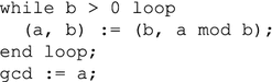
Design a circuit to compute the greatest common divisor of two natural numbers, based on the following simplified Euclidean algorithm.

-
4.
Design a circuit for computing the greatest common divisor of two natural numbers, based on the following Euclidean algorithm.
-
5.
The distance d between two points (x 1, y 1) and (x 2, y 2) of the (x, y)-plane is equal to d = ((x 1 − x 2)2 + (y 1 − y 2)2)0.5. Design a circuit that computes d with only one subtractor and one multiplier.
-
6.
Design a circuit that, within a three-dimensional space, computes the distance between two points (x 1, y 1, z 1) and (x 2, y 2, z 2).
-
7.
Given a point (x, y, z) of the three-dimensional space, design a circuit that computes the following transformation.
$$ \left[ {\begin{array}{*{20}c} {x_{t} } \\ {y_{t} } \\ {z_{t} } \\ \end{array} } \right] = \left[ {\begin{array}{*{20}c} {a_{11} } & {a_{21} } & {a_{31} } \\ {a_{21} } & {a_{22} } & {a_{32} } \\ {a_{31} } & {a_{32} } & {a_{11} } \\ \end{array} } \right] \times \left[ {\begin{array}{*{20}c} x \\ y \\ z \\ \end{array} } \right] $$ -
8.
Design a circuit for computing z = e x using the formula
$$ e^{x} = 1 + \frac{x}{1!} + \frac{{x^{2} }}{2!} + \frac{{x^{3} }}{3!} + \cdots $$ -
9.
Design a circuit for computing x n, where n is a natural, using the following relations: x 0 = 1; if n is even then x n = (x n/2)2, and if n is odd then x n = x·(x (n−1)/2)2.
-
10.
Algorithm 2.4 (scalar product) can be implemented using more than one interleaved_multiplier. How many multipliers can operate in parallel? Define the corresponding schedule.


References
Hankerson D, Menezes A, Vanstone S (2004) Guide to elliptic curve cryptography. Springer, New York
Deschamps JP, Imaña JL, Sutter G (2009) Hardware implementation of finite-field arithmetic. McGraw-Hill, New York
López J, Dahab R (1999) Improved algorithm for elliptic curve arithmetic in GF(2n). Lect Notes Comput Sci 1556:201–212
Author information
Authors and Affiliations
Corresponding author
Rights and permissions
Copyright information
© 2012 Springer Science+Business Media Dordrecht
About this chapter
Cite this chapter
Deschamps, JP., Sutter, G.D., Cantó, E. (2012). Architecture of Digital Circuits. In: Guide to FPGA Implementation of Arithmetic Functions. Lecture Notes in Electrical Engineering, vol 149. Springer, Dordrecht. https://doi.org/10.1007/978-94-007-2987-2_2
Download citation
DOI: https://doi.org/10.1007/978-94-007-2987-2_2
Published:
Publisher Name: Springer, Dordrecht
Print ISBN: 978-94-007-2986-5
Online ISBN: 978-94-007-2987-2
eBook Packages: EngineeringEngineering (R0)