
Abstract
Silicon photonics is nothing new. It has been around for decades, but in recent years, it has gained traction as electronic design challenges increase drastically with their atomic-level limitations. Silicon photonics has made significant advancements during this period, but there are many obstacles without an acceptable level of comfort as seen by the lack of semiconductor community involvement. Apart from a series of technological barriers, such as extreme fabrication sensitivity, inefficient light generation on-chip, etc., there are also certain design challenges. In this chapter, we will discuss the challenges and the opportunities in photonic integrated circuit design software tools, examine existing design flows for photonics design and how these fit different design styles, and review the activities in collaboration and standardization efforts to improve design flows.
Access provided by Autonomous University of Puebla. Download chapter PDF
Keywords
These keywords were added by machine and not by the authors. This process is experimental and the keywords may be updated as the learning algorithm improves.
4.1 Silicon Photonics—History Repeats Itself
Integrated photonics has been around for many years, and like the electronic semiconductor industry, it continues to evolve and change. Its progression is similar to electronics with a progression from discrete products assembled on a printed circuit board to more highly integrated circuits.
In the late 1970s and early 1980s, there was a significant shift in the electronics market in the designing of custom integrated circuits. The shift came in the form of the use and reuse of pre-characterized building blocks or “cells” as opposed to designing each transistor from scratch for each new chip. This technique later became known as “standard cells” or cell-based design, and it became the standard way used to build application-specific integrated circuits (ASIC s).
At the same time, there was a major shift in the methodology used to design and verify integrated circuits (ICs). General-purpose computing and engineering workstations were becoming available to the engineering community in conjunction with the advent of computer-aided design (CAD) tools. Later, this turned into an entire industry now known as electronic design automation (EDA ). Additionally, over the next several decades, hierarchical design and test methodologies [1] were codified, taught, and used to progressively enable scaling of IC design complexity from small-scale integration (SSI) to very large-scale integration (VLSI) and to what we now know as system on chip (SoCs).
Photonics is now in a similar state as to what the IC industry was in the early 1980s. There is a desire in the industry to integrate photonic components onto a common substrate and to bridge these photonics with their electrical counterparts monolithically either on the same die or on a separate die, but within the same package. Like the IC design in the early 1980s, there is now a need to codify design methodologies and to put into place the necessary industry ecosystems to support the scaling, both technical and economical, of integrated photonic design, manufacturing, and testing.
The good news for the industry is that engineers can leverage much of the infrastructure and learning that has gone into the electronics IC industry over the last 30 years.
4.2 Photonic Integrated Circuit Design Methodologies and Flows
Integrated photonic circuit design follows much the same design methodology and flows as traditional electrical analog circuit design. However, there is still a weakness in the photonic design process, and that is a successful circuit-like, schematic capture , approach. Even today, many photonic engineering teams with considerable design expertise start from the layout. Unlike digital electrical design, it is not easy to abstract the circuit into simple logical gates synthesized from a high-level design language. Instead, the circuit is envisioned at the system level and usually modeled at that level with tools like MATLAB [2], C-coded models, Verilog-A [3], or scattering matrices . Once an engineer designs the high-level function, it is then up to the optics designer to partition the design and map it into photonic components realized in the integrated circuit. This mapping process is typically a manual task and involves many trade-offs based on the material and the fabrication facility to be used to manufacture the product. Eventually, the design is captured and simulated with physical effects of the material being taken into account. After the physical design is complete, the design is checked for manufacturing design rule compliance and then passed on to the fab in industry standard GDSII format to be manufactured.
4.2.1 Front End Versus Building Blocks Methodology
As with electronic design of the late 1970s, it is not uncommon for photonic designers to bypass logic capture and go straight to physical design of individual components. In many cases, each component is laid out and simulated with mode solvers and propagation simulators to ensure that the component’s design meets the designer’s intent. These steps repeat for each component and then the designer places and routes the entire circuit together and resimulates with a circuit simulator using compact models for the components derived from the physical simulations or measurements.
As explained in the introduction, many designers continue to start from layout (front end). But as the photonic circuit becomes larger and more complex, it becomes essential to start from the circuit or logic level (using photonic building blocks to construct a photonic circuit), where system specifications dictate how to build the circuitry. Specialization occurs: some photonic designers focus on the physical properties of single components (e.g., MMIs , waveguide bends, MZIs , splitters, rings, etc.) and perform physical simulations. Others concentrate on the logic level, where circuit simulations use compact models .
Circuit simulation is possible, because, different from RF design, the dimensions of most building blocks are larger than the wavelengths of interest. In most cases, this allows a logic separation of the building blocks. Optical waveguides are used to connect the building blocks, and act as a dispersive medium.
4.2.2 Process Design Kit Driven Design
It was at the end of the 1980s and in the early 1990s that integrated photonics research started to surface and become visible to a wider audience. Materials like polymers, doped glass, and dielectric thin film materials like silicon oxide and nitride were dominant at that time. This new emerging field was called integrated optics, studying lightwave devices or planar lightwave circuits (PLC). As a result of these research activities, a need for proper design software emerged focusing on the simulation of mostly passive optical structures at the micrometer scale and the mask layout for the actual fabrication of the structures and devices. This was reflected in the start of an annual conference on Optical Waveguide Theory and Numerical Modeling (OWTNM ) in 1992, and the first commercial activities for design services and simulation tools (BBV [today PhoeniX Software ] in the Netherlands in 1991 and PhotonDesign in the United Kingdom in 1992).
As with electronic design moving into the 1980s, the optic design flow is now giving way to a more traditional flow as used by electrical analog design. Since the early 1990s, photonic IC design software has developed into what is available today; a set of more or less integrated solutions from a variety of vendors covering different levels in what is called the photonics design flow (PDF) or photonics design automation (PDA). The required software tools to create a full PDF or PDA include circuit simulators, mask layout tools, measurement databases, and design rule checkers. However, they also include physical modeling tools such as mode solvers and propagation simulators .
From the beginning, the designers in the field of integrated photonics have been working with a bottom-up approach, starting with the fabrication technology and materials and taking these as a starting point to develop integrated photonic devices. With the introduction of more standardized and generic fabrication processes since 2005 and the resulting creation of process design kits (PDKs , also called physical design kits) (see Sect. 4.5.3), a mixed design approach has evolved in which a group of designers develop the contents of the PDKs and a second group of designers use these PDKs in a top-down approach starting from the system or circuit level.
There are more fabrication facilities becoming available for complex photonic designs. The fab-provided PDKs contain documentation, rule “decks” for verification software, process information, technology files for software, a device library of basic devices (referred to as “PDK cells”) that are validated by the process, and layout guidelines for designing custom devices (further referred to as “user cells”). These PDKs are developed and maintained by the fabrication facility and include plugins for commercial CAD tools. Depending on the application or completeness of the foundry PDK , photonic designs make heavy (like digital IC design ) or light use (like analog IC design ) of PDK cells vis-à-vis user cells. Nevertheless, compared to the digital IC design flow, fabrication facility-provided photonic PDKs today address few aspects of a complete design flow and contain a limited device library.
Once a designer chooses a technology platform, they are required to obtain the PDK for that technology, which gives the designer everything needed for the physical design of the chip, including custom device design. For example, each technology will specify a recommended typical and minimum bend radius for the waveguides (below which the bend will lead to sizable waveguide loss). Alternatively, process tolerance information like the maximum width deviation of the waveguide core can be ±1 nm. The designer needs to take all these rules and guidelines into account when laying out custom cells. On the other hand, the library of validated cells allows for top-down design. Compact models enable the designer to make the connection between the higher level circuit design and the devices available in the technology of interest, without needing to resort to electromagnetic or device simulation.
Photonic PDKs contain various cells and templates, proven to work for a certain wavelength. Here are a few examples:
-
[fixed cell] A grating coupler , used to couple light from an optical fiber (vertically) in/out of the chip. Different cells may exist with each designed and tested for various wavelength ranges.
-
[fixed cell] A 3 dB splitter, used to split input light into two channels (50 %/50 %).
-
[templates] Waveguide templates, which specify the cross section of a waveguide (i.e., thickness of the core and slab region), typically designed to offer minimal loss.
-
[fixed cell] A high-speed PN junction-based MZI modulator.
-
[custom cell] Typical custom cells are introducing filtering and processing of the optical signal s. A widely applied custom cell or parametrized photonic building block is the arrayed waveguide grating (AWG ). This AWG , in fact, acts as a MUX or DEMU X and can contain up to hundreds of waveguide sections.
The PDK -supplied rule decks for DRC and LVS enable the designer to verify his design against design rules and ensure consistency between schematic and layout prior to sending the design to the fab.
Several key items in the above description are still under active development. In particular, today’s silicon photonic PDKs most often lack compact models for devices and, while LVS for photonics is still being developed, a few early rule decks do exist.
In conclusion, PDKs allow the user to carry out the physical implementation of the design, based on building blocks made available by the fab combined with custom designed cells based on given design rules.
4.2.3 Overview of Flow—Comparison to Analog Design Flow
With the advent of predefined photonic components and multiple foundries, the design flow and the methodologies used to create photonic integrated circuits (PICs) become directly analogous to electrical analog design. The foundry collects the predefined components into a PDK that is developed and maintained for each of their supported photonic processes. Once a PDK is installed the photonics designer can select from the PDK cells and instantiate and place their multiple copies, adjust their parameters when provided, and then connect them together with waveguides. As designs become more complex, the PIC designer can employ the use of hierarchy, which allows for the copy and reuse of blocks or “cells” of connected custom components with well-defined interfaces, throughout a design. These user cells can be documented and stored for reuse by other designers. In the electrical design world, this collection of cells is typically called a library. A PDK is a distinct type of library as it is a set of programmable cells (pcells) that come directly from the foundry and are already pre-characterized.
Furthermore, designers are now working with more third-party foundries to make predefined and characterized components available, best tuned for the selected foundry process. Unlike digital design, these components are not static but instead are parameterized to allow the optics designer to be able to dial-in certain parameters to meet design requirements. Once the parameters are set, the programmable device autogenerates the component layout along with a compact model used for circuit-level simulation. As with electrical analog design, these programmable components also check for valid ranges of input parameters for which the compact models will be valid. The idea is to use as many of these predefined components as possible to reduce risk and time required to create the detailed, yet fab-compliant, layouts and fab-qualified models. Such libraries are being developed with photonics designers or CAD tool vendors in collaboration with the fab.
4.2.3.1 Schematic-Driven Layout
With the increase in complexity, many designers wish to capture their circuit at the logic level before spending a considerable amount of time creating layout. This desire is directly analogous to analog design in the electrical world. Instead of jumping right to layout after system design, the designer captures the design in a schematic abstraction of the circuit. The symbols used in the schematic have a direct one-for-one relationship with the programmable components used during layout. The CAD flow automatically makes a connection between the logic symbols and the correct compact models for circuit simulation. The symbols are placed and connected together with abstractions for the waveguides, ideal parameters are set on the components and waveguides in the schematic, and then the circuit is simulated. The designer iterates on the design, changing parameters on components, adding or removing components, and resimulating until all design objectives are met.
The benefit of using the abstracted level of the design at this stage, is that it allows the designer to focus on getting the circuit to function as desired without getting bogged down in the details of layout design rules, layout placement, and shaping of individual waveguides that can be very time-consuming. The idea is to avoid spending too much time crafting placements and waveguides only to find out that the basic circuit still is not functioning.
Once the PIC designer is satisfied that the design is converging, the layout process can begin. Electrical designers have learned over the years that it is best to use a methodology known as schematic-driven layout (SDL ). SDL employs a correct-by-construction (CBC) methodology whereby the CAD tools do not allow the designer to layout and connect up something that does not match the connectivity of the schematic design.
SDL also ensures that all parameters used during the schematic design get used for the correct generation of the programmable components, so there are no surprises caused by accidentally using the wrong parameters on the optical layout components. At this stage, we want the designer focused on the best possible placement of the components that allows for straightforward connections by the necessary waveguides and avoiding interference between multiple neighboring components.
Since the designer must work in a confined 2-D environment, there will most likely be some parameters or constraints that were forward annotated from the schematics to the layout that cannot physically be met; these could be, for example, nonverified user cells. When this happens the CAD flows must allow the designer to adjust parameters in the layout and then back-annotate these changes into a view of the schematic that can be resimulated.
4.2.3.2 Design for Test and Manufacturability
At the current stage of integrated photonics, the concepts of design for test (DFT ) and design for manufacturing (DFM ) have not been well addressed. Most fabrication facilities have limited DFT sites to test the functionality of PDK cells for wafer qualification. As silicon photonic circuit design complexity increases, netlist -driven automated DFT site generation will be increasingly important. DFT development will follow a mature SDL environment. DFM in silicon photonics today consists only of basic design verification comprising rules for shapes of polygons within a process layer (width, space, diameter, etc.), and rules for inter-process layer alignments (overlaps, enclosures, etc.). The current DFM maturity is only sufficient for checking the manufacturability of the design but not its yield, functionality, or reliability. (In commercial manufacturing sites, mainly PLC and InP, these things are in place.)
Like electronic design, the design specialty field of DFT and DFM for integrated photonics will eventually be required, especially as the design complexity for integrated photonics continues to grow. DFM will be of particular interest to photonic designers, as subtle changes in the process can have dramatic effects on the performance and functionality of photonic components. As the integrated photonics industry matures, additional work to characterize areas of yield loss will be required, and methods will need to be created for optics designers to design in such a way for the designs to be robust to process variations.
4.2.3.3 Design Sensitivity
For interferometric devices, the phase relationship between two waveguide paths determines the overall behavior of the device; examples include ring resonators , Mach–Zehnder interferometers , and so on. This behavior is quite comparable to RF design, where the exact wire length and shape largely affect the overall behavior.
Even more so, the fabrication tolerances are very strict. A 1 nm change in waveguide width can cause a 1 nm shift in filter response [4]. A 1 nm shift, at a wavelength of 1.55 μm, corresponds to a frequency shift of 125 GHz, which is sufficient to span more than one channel in a typical wavelength division multiplexing (WDM) device. The same holds for temperature changes: a temperature change of roughly 12 K corresponds to the same 1 nm shift [5].
For this reason, smart designs can be made that compensate for design tolerances [6], which are a real challenge for designing photonic chips that contain interferometric devices. Good control over the waveguides line shape in the technology process, together with clever engineering, can reduce the risks for not obtaining the targeted specifications. For more information, see Sect. 4.3.1 on silicon photonics fabrication processes.
4.2.4 Schematic Capture
A schematic is an abstracted view of the circuit at the logic level. The objects placed in the schematic can come directly from a foundry PDK or could be symbols created by the designer that represent more levels of design hierarchy. Schematics serve many purposes. They are used to capture the implemented logic, as well as design intent. Design intent can be in many forms, but the most common are simple textual notes that record the designer’s assumptions. Designers also annotate their schematics with instructions for how the associated layout should handle various components. In both electrical and photonic domains, designers annotate parameters on the instances of schematic components that use both the simulation and the layout of the actual component.
More advanced schematic capture packages also allow the designer to represent repeated structures in very compact forms like buses and “for loops” that contain circuit components. Schematics are meant to be printed, and when circuits get too large they cannot be represented on one schematic. There are special annotations that allow the designer to continue the design on more pages of the same schematic hierarchy. Similarly, there are conventions that can be used to simplify the schematic drawing so that referencing connections is made between components on opposite sides of the schematic by name instead of having to route a line between them. The idea here is to make capture of the logic accessible so that the designer can get to simulation and debug of the circuit behavior quickly—the less drawing and more debugging, the better. To deal with hierarchy, the CAD tools make use of the concept of pins and ports on components as a way for the software to keep track of connections between levels of hierarchy and connections from page-to-page. At a given level of the hierarchy, “ports” are defined as the interface for the cell being designed. Once the cell is complete, the CAD tools have automated ways to create an abstracted symbol for the cell. The symbols have “pins” which are connection points for the symbol. There is a one-for-one correspondence for ports in the schematic for each pin on the symbol. Typically, these associations are done by name on the port and associated pin. A newly created symbol for a schematic placed in a library, instantiated, and then used in other levels of the design hierarchy, helps the user to abstract the design at any level of hierarchy to something that is meaningful to anyone else who reads the schematic.
4.2.4.1 Interface to Simulation and Analysis
In both the electronic and photonic domains, designers employ circuit simulators to verify and debug the function of their designs. The schematic serves as a way to capture the circuit in a form that the simulator can use through steps known as elaboration and netlisting. A netlist is a non-graphical representation (and typically human readable) of the connectivity of the design. Netlists can be hierarchical or flat and typically carry the property information needed by downstream tools like simulators and layout generators. Elaboration is the step that unwinds the higher levels of abstraction into specific instances that will be simulated and generated in the layout. An example of this in electronic design is when the designer uses something called a multiplier factor parameter or “M factor ” parameter [7]. A transistor symbol, with an M factor of 4, means that the designer will actually get four transistors for the one abstracted symbol in the schematic. Each of these four transistors connects in parallel, and each will have the same properties as assigned to the symbol on the schematic. The elaboration step expands the one transistor into four in the netlist and makes sure that all of the appropriate properties are on each of the new instances.
In addition to the netlist , simulators also need a variety of inputs from the user. This would include things like identification of circuit input and output terminals for the simulation, identification of signals that the designer wishes to monitor for viewing in a waveform viewer, and other analysis points on the circuit that the user may want the simulator to monitor and output for debug purposes. The user interface for this is typically integrated with the schematic to make it easy for the designer to identify graphically nodes of the circuit as opposed to having to type in terminal names. The CAD tools also have graphical interfaces to allow the designers to map the symbols to different levels of simulation models allowing for mixed-level simulations. Not all simulators are capable of this, so the CAD tools typically have dialog boxes that are unique to the chosen simulator. This user interface allows the designer to use the same schematic capture system for high-level systems design, circuit design, and mixed mode simulations where parts of the circuit are still at behavioral levels while other areas of the circuit are at the component level.
In more advanced design flows, the netlister and elaborator are also responsible for forward annotating constraints captured by the designer in the schematic on to the layout generation tools. The netlister and elaborator take care of all of the internal connections that must be made between the different editing tools so that the designer can focus on design and not tool integration complexities.
4.2.4.2 Matching Simulation to Layout
A general methodology used by electrical designers is to design their analog circuit first as an ideal circuit. Ideally, in this case, it means that the designer debugs the circuit without taking into account the physical effects of component placement and the parasitics due to routing. In this case, the circuit is simpler in nature, and it should be easier to tune the design to get the desired response. The same is true in photonics design. Wires connect the major components in the schematic. These wires represent waveguides in the layout. The parameters of the abstracted components and waveguides are set by the designer in the schematic and then work using the simulator to bring the circuit to the desired behavior.
Once this step is close to completion, the designer then moves to layout. The idea here is that the parameters used in the ideal circuit are forward annotated to the layout system where a CBC layout methodology is used to try to meet the original assumptions of the designer. Presumably, if the designer can meet the original assumptions, then the post-layout simulations of the virtual layout should match the simulations of the idea circuit. Matching the original circuit simulation and post-layout simulation can be challenging, and this is especially true for photonics. In photonics, this is because the phase has to be controlled precisely (e.g., in Mach–Zehnder interferometers , ring resonators , etc.). Phase is a function of the topology and materials of the components and waveguides, and the designer is not yet aware of these at schematic capture time. The CBC methodology proposes that the phase relationships are passed on to the layout tools, which would then try to construct the components and waveguides in such a way that the phase relationships are maintained. Depending on the overall circuit, this may not be possible. In which case, some of the parameters on the components and waveguides will need to be changed to accommodate the physical constraints of the area allowed for the layout. When this happens, the CAD tools must have a mechanism to back-annotate and merge the changed parameters of the layout with the original parameters of the ideal design. This data is stored as a revision of the netlist so that the original ideal circuit description is not lost. The revised netlist can then run against the same simulation test benches used to debug and characterize the ideal circuit. A designer then compares the results between the ideal circuit and the virtual layout and any issues caused by the changes must then be resolved either by changing the layout or by changing the logic circuit to be more robust to the physical effects and ultimately reiterating the design.
4.2.5 Photonic Circuit Modeling
Numerical modeling is an essential part of any modern circuit design, whether electrical or photonic. A designer performs simulations to optimize the circuit and ensure that it will meet its performance requirements. Also, circuit simulation can provide information on circuit yield if the effects of realistic manufacturing imperfections can be correctly taken into account, allowing the designer to optimize the circuit for manufacturability. The key requirement of circuit simulation is that it must be predictive, or in other words, that the results of the circuit simulation agree to sufficient accuracy with the actual circuit performance after manufacturing.
4.2.5.1 Electronic Simulations Using SPICE
For electronic circuits, SPICE is the de facto standard for simulating resistors, capacitors, and inductors (RLC circuits) better known as linear electrical circuits. Moreover, there are many methods for modeling nonlinear devices, such as diodes and transistors, by linearizing them around operating points. A SPICE tool can then simulate the small-signal frequency domain or (transient) time domain behavior of the circuit. On a higher level of abstraction, Verilog-A can be used to describe the input–output relationship of an arbitrary component and, at the system level, IBIS can be used for modeling communication links with SerDes devices [8]. Advanced simulation strategies can then seamlessly interpret all this information and perform a coherent simulation.
4.2.5.2 Electronic Versus Photonic Simulation
Similar to electronic circuit simulation, photonic circuit simulation commonly requires both transient and scattering data analysis to model signal propagation within the time and frequency domain. Therefore, one approach has been to reuse circuit simulation algorithms originally designed for the simulation of electrical circuits such as SPICE [9]. However, as photonic circuits are physically described using wave phenomena, it is not straightforward to map this onto an SPICE-like formalism, which assumes that the wavelength of the information carrier is much larger than the size of the components and can be treated as lumped elements. Typical photonic circuits exist of several building blocks, which themselves are often larger than the signal wavelengths: the signal wavelengths are in the visible to near-infrared (i.e., 700 nm–10 µm, with 1.3 µm, and 1.55 µm the most commonly used wavelength bands for data and telecom applications). In contrast, individual building blocks can be of the size of ~10–1000 μm2, depending on the technology.
Unlike electrical circuit simulators, photonic circuit simulators must take into account the complex nature of light that includes the optical signal’s polarization, phase, and wavelength. The optical simulation and analysis of PICs is particularly challenging because it involves bidirectional , multichannel , and even multimode propagation of light and waveguide connections between consecutive components require specialized treatment unlike that done for electrical traces [10]. In addition, photonic circuit components often involve both electrical and optical signals , and there is still little standardization for how to perform the necessary, mixed-signal simulations in the time domain. Lasers , modulators, couplers, filters, and detectors are just a few of the different components present in a complete PIC . Each of these components has different operation principles that are highly dependent upon the particular process, technology, and physical geometry. Photonic circuit simulators, therefore, must rely on proper compact models , calibrated for a particular foundry process, which accurately represent the optical and electrical responses of these components in the time and frequency domains.
4.2.5.3 Photonic Circuit Simulation
Photonic building blocks or components are linked using waveguides that guide optical signals . They are represented as a delay line, adding delay and phase to the signal. To complicate matters: both the group delay and the phase delay can be very dependent on the signal wavelength, and multiple wavelength carriers can be used simultaneously in the same waveguide circuit.
In a photonic circuit simulation, each component (including waveguides) is represented by a black box model with input and output ports and a linear or nonlinear model describes the relationship between the ports. The larger photonic circuit contains the collection of these building blocks, connected at the ports, with a given connection topology. These connections are purely logical (Figs. 4.1, 4.2, 4.3 and 4.4).

Multiple schematic views of simulations

Detailed layout placement of a design

Schematic-driven layout ensuring a correct-by-construction layout

Example of photonic pcell—elaboration passes appropriate parameters to simulation and layout
Designers implement the building block model description in different ways: purely linear, frequency domain based, or a more complex description for time domain and/or nonlinear interaction. For the linear part, matrix formalism can be used. The two most commonly used formats are
-
(1)
Transfer-matrix methods: in this case, the assumption is made that there is a set of input and a set of output ports. The output ports of component 1 cascade to the input ports of component 2. This method is simple and easy to understand (and can be easily implemented, e.g., in MATLAB or Python), but it has the drawback that no reflections or feedback loops are possible.
-
(2)
Scattering matrix methods (see Fig. 4.5): here, reflections and feedback loops can be taken into account. As most photonic circuitry will contain these two effects, it will lead to a more accurate result. For complex circuitry, it quickly becomes beneficial to adopt the scatter matrix formalism. A mathematical description of how to calculate the system response based on individual scattering matrices can be found in [11].
Fig. 4.5 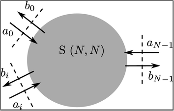
A N-port linear component can be represented by an (N, N) scatter matrix S. The input signals (represented by the input vector a) are related to the output (represented by the vector b) using the following equation: b = S a

Time domain models that take nonlinearities into account can augment both methods. The main advantage of this approach is the natural representation of variables such as temperature, carriers (e.g., the plasma dispersion effect), and resonator energy (for coupled mode theory models), making it simpler to interpret these models.
When combining photonic circuits with electronic circuits, it is not trivial to balance the two different simulation strategies. One approach is to reduce the photonic model to a description that a designer can implement into Verilog-A then simulate using an electronics simulator. This approach requires that some photonic quantities, such as optical power and phase, map into native Verilog-A variables. Also, more elaborate information of the photonic model, such as multiwavelength behavior, polarization, etc., are not taken into account, or need to be simulated as a parameter sweep. Such a compact model can work well in a small operation region (i.e., for a fixed wavelength, temperature, and voltage). As long as this model satisfies the need for a particular application (e.g., single-wavelength optical interconnects ), this approach can be used for the co-simulation of photonics and electronics. The challenge is to find a good compact model that is valid over the operation region of the circuit. This simulation strategy has the lowest threshold for electronic engineers engaging in the field of photonics and has some limitations as described.
It is worth noting that while some electrical simulators support scatter matrices (which can map onto an RLC circuit), the shape of the response will determine accuracy. Moreover, nonlinearity/reflections are not easy to model accurately.
4.2.5.4 Frequency Domain Analysis
Frequency domain analysis is performed using the same type of scattering analysis used in the high-frequency electrical domain for solving microwave circuits, enabling bidirectional signals to be accurately simulated [12]. This approach can be extended to allow for an arbitrary number of modes in the waveguide with possible coupling between those modes that can occur in any element. Consequently, the scattering matrix of a given element describes both the relationship between its input and output ports and the relationship between its input and output modes. The advantage of frequency domain analysis is that it is relatively standardized. The so-called S-matrices for each component (including possible coupling between modes on the same waveguide ports) are all that is required to perform a frequency domain simulation of the circuit. However, the frequency domain simulation, while very valuable for a broad range of design challenges, is insufficient for most circuits and systems that make use of active components, which require the simulation of both electrical and optical signals .
4.2.5.5 Time Domain Analysis
Unlike frequency domain analysis, there is little standardization in time domain analysis. For time domain analysis, it is necessary to represent multichannel signals in multimode waveguides with bidirectional propagation . These waveguide modes must not limit polarization states to only two, which are a clear distinction, compared to many fiber-optical systems. Also, there must be the ability to support both electrical and digital waveforms since, for example, an electro-optical modulator must take both electrical and optical inputs to produce a modulated optical output.
One approach is to use a dynamic data flow simulator. When a simulation runs, data flows from the output port of one element to one or more input ports of one or more connected elements. When an element receives data, its compact model applies the element’s behavior to the data and generates the appropriate output. In the time domain simulation, data can be represented as a stream of samples where each sample represents the value of the signal, either optically, electrically or even digitally, at a particular point in time. This approach has the flexibility to represent different element behaviors and signal types, which enables the development of compact models that can comprehensively address the variety of active and nonlinear optoelectronic devices present in photonic integrated circuits .
This type of simulation approach used in combination with electrical circuit simulation methods such as SPICE is the simplest method to run separate electrical and optical simulations, and exchange waveforms between them, and this approach has been demonstrated successfully [13]. In the future, it will likely be necessary to extend this to a full co-simulation approach whereby the photonic circuit simulation runs in a larger scale electronic simulation.
The time domain signal integrity analysis of a circuit under test is performed by analyzing the input or output signal at different ports, which may be electrical, optical, or digital. A typical result from a time domain simulation is the eye diagram , as shown in Fig. 4.6. The analysis of the eye diagram offers insight into the nature of the circuit imperfections. The time domain simulation can calculate the eye diagrams, and the resulting analysis can determine key signal integrity parameters such as bit error rate (BER) , optimum threshold and decision instant, and extinction ratio. As increasingly complex modulation formats become more widespread, such as quadrature phase-shift keying (QPSK), calculating constellation diagrams will produce the best signal integrity analysis. An example of the eye diagram and constellation diagram from a simulation of an optical QPSK with electrical 16-QAM (quadrature amplitude modulator ) system is shown in Fig. 4.8 as part of an example circuit.

The eye diagram resulting from a simulation of an optical transceiver
4.2.6 Model Extraction for Compact Models
The compact models required for PICS modeling must be generated using a combination of experimental results and accurate optical and electrical physical simulation. If the optical component is passive and linear, it suffices to provide a scattering matrix (typically wavelength dependent). Devices with dynamical behavior will need more complex models (e.g., an optical phase modulator will require the electrical voltage over the p(i)n diode as additional input).
In the case of passive components, the scattering matrix can be obtained by performing a full physical simulation (e.g., finite-difference time domain [FDTD ]). Previously, fabricated components can be measured to obtain a wavelength-dependent spectrum.
From the given spectrum, compact models can be made that represent the original component, within a given accuracy. Measurement noise has to be eliminated in order to create a useful model in cases where a designer obtains the spectrum from a measurement. Passivity and reciprocity are essential properties of the model obtained.
One example of creating these models is the vector fitting method [14]. With this method, an arbitrary S-matrix is approximated with a set of poles and zeros. Some challenges with this method are to find a good filter order and to cope with nonsymmetry of the optical filters due to dispersion.
A second example is to model scattering matrices using FIR filters, which have more degrees of freedom than IIR filters, but are computationally more demanding to execute. In the case of active components, the model, characterization, and parameter extraction need to be tailored for each component. For example, an optical laser can be described using rate equations [15]. Optical phase modulators have a voltage-dependent transmission, described as a series of steady-state, voltage-dependent scattering matrices , or with a more dynamical model, where the transmission is dependent on the number of free carriers in the p(i)n junction, and an ordinary differential equation (ODE) simulates the number of free carriers. All of these methods are vital when building robust PDKs (see Sect. 4.2.2).
4.2.6.1 Methods and Challenges
Waveguides are an excellent example of components that require a combination of simulated and experimental data. A mode solver, knowing the cross-sectional geometry, can generate the effective index, group index, and dispersion. It is possible to calculate the dependence of these quantities on geometric changes such as waveguide width and height, as well as external influences such as temperature, electrical fields, or mechanical stress. However, the waveguide loss, in a well-designed geometry, comes primarily from sidewall roughness. While it is possible to simulate these losses if enough information on the roughness measurements of surfaces (RMS) and correlation length is known, in practice, it is much easier to use experimental waveguide loss results when creating the compact model.
4.2.6.2 Model Extraction from Physical Simulations
Similarly, the majority of passive component compact models can be calibrated using a combination of simulation results and experimental data. For example, when creating a compact model for a splitter, the insertion loss (IL) may come directly from the experimental data. However, even well-designed splitters have a small but nonnegligible reflection that is challenging to measure directly. In this case, a simulation of the design can provide the reflection and the phase of the S-parameters while confirming the experimental IL data. As with waveguides, the simulation can provide sensitivity analysis, such as the dependence of parameters on waveguide thickness, which may be challenging to obtain experimentally.
4.2.6.3 Compact Models in the Time Domain
Compact models for electro-optical modulators for time domain simulations are much more challenging. To simulate a Mach–Zehnder modulator requires, at a minimum, the waveguide effective index and loss as a function of bias voltage calculated by a combination of electrical and optical simulations, where the electrical simulations must be calibrated against experimental data such as the capacitance versus voltage curve. Excellent agreement with experimental results with a DC bias can be obtained [16] once calibrated, as well as with the spectral response under different bias conditions [17].
For time domain simulations, the compact model must be able to respond to time-varying electrical and optical stimuli. When driven at higher frequencies, the Mach–Zehnder modulators frequently have complex effects that must be accounted for, such as: impedance mismatches of the transmission line and the feeds; improper termination of the transmission line; and velocity mismatches of the transmission line and the optical waveguide. To accurately simulate a modulator driven by an electrical bit sequence that contains frequencies from DC to 10s of GHz and beyond, it is necessary to calibrate carefully the models to account for these effects.
The photodetector responsivity versus bias voltage is often measured experimentally under continuous-wave (CW) illumination , and this data can be used to create the compact model. The high-frequency behavior can be recreated using a filter with parameters calibrating against experimental data. Similarly, the dark current is often measured experimentally. The temperature dependence of these quantities can be obtained experimentally if available, or it is simulated with a combination of optical and electrical solvers.
4.2.6.4 Photonic Circuit Modeling Examples
A typical circuit analyzed in the frequency domain is an optical switch [18, 19]. These circuits can include hundreds of components due to all the waveguide crossings that are required. An example circuit diagram is shown in Fig. 4.7, which also makes it clear that the larger the number of elements, the more necessary the circuit hierarchy becomes.

Circuit diagram for an optical switch
The entire circuit is displayed together with a zoomed view of a portion of the circuit including the optical network analyzer. Also shown, is the inside of a subcircuit element that includes a large number of waveguide crossings. The entire circuit contains hundreds of elements. Nevertheless, the results of the optical network analyzer can be calculated in less than a minute over a typical range of frequencies.
In the time domain, a typical circuit to simulate is a transceiver [20]. In Fig. 4.8, a 16-QAM transmitter is shown along with the resulting eye and constellation diagrams.

A circuit diagram for an optical QPSK with an electrical 16-QAM system is shown in (a). The resulting eye diagram is shown in (b), and the constellation diagram is shown in (c). Elements of the displayed circuit diagram are themselves subcircuits, which contain a number of elements
4.2.7 Schematic-Driven Layout
In photonics, historically most emphasis has been on the full-custom layout of the individual components and combining these into (simple) circuits. Today, with the increasing complexity of the circuits the mask layout ideally should be generated from the schematic, as created with a circuit design tool.
Schematic-driven layout (SDL ) is a methodology and design flow whereby the layout tool continually checks the connectivity of the layout against the connectivity of the elaborated netlist . If the designer tries to connect up something in the layout that is not in the elaborated netlist , the CAD tool will flag the issue to the designer. In some companies, policies are put in place whereby the CAD tool is set up to not allow changes to the connectivity within in the layout tool. The schematic must include any connectivity changes which forces the designer to remember to rerun simulation verification on the new netlist . Other companies find this too restrictive and allow for design connectivity changes made directly in the layout. This practice, however, should be discouraged, as it is very difficult to back-annotate design changes from the layout to the schematic. It should also be noted that since CAD tools can be set up to allow for different change scenarios, SDL should not be relied upon as the last check before manufacturing to ensure the circuit layout is connected up. It is the responsibility of the designer to both resimulate the design and to run physical verification tools that perform a more exhaustive check of all layout versus schematic connectivity.
In addition to checking connectivity, the SDL flow is also responsible for setting parameters of any programmable layout cells (pcells ) forward annotated from the schematics. It should be noted, at this point, that the hierarchy of the layout does not need to match the hierarchy of the schematic. If this is the case, the CAD tool is responsible for all name and parameter mappings between the two hierarchies. CAD tools that handle this methodology typically have a hierarchy browser that lets the designer cross-probe between the schematic and the layout views even when the hierarchies of the two views are different.
The benefit of using an SDL -based design methodology becomes clear when design sizes increase, especially when a team of designers is working on a project as opposed to a single designer. Different people usually do circuit design and layout design. Using SDL ensures accurately communicated design connectivity between the schematic and layout stages. A second benefit of using an SDL -based flow is that last minute design changes can be tracked by the CAD system to ensure that the changes made in the layout are, in fact, the same changes that are in the schematic. The CAD tool will flag the differences it sees in the layout versus the newly updated schematic.
CAD tools ensure that connectivity is correctly preserved in the layout tool using the SDL -based flow that enables the use of more advanced constraint-driven layout engines such as pcells, auto-placement, and autorouting.
The SDL strategy is well developed in electronics, using semiautomated algorithms for placing “functional pieces” and routing the connecting “wires”. Electronic design is very suitable for this since, in most designs, the wires can be considered as “just a connection” and they do not influence the overall design, for example, due to increased delay times. For many low(er) speed applications, the electric wires on the chip are just a low-loss way to transmit signals. Therefore, the placement of the functional parts with nonoverlapping wires between the different pieces is a purely geometrical problem. This simple concept requirement is frequently solved using autorouting approaches of the wires, where the paths are typically vertical or horizontal (Manhattan ) routing patterns. Nowadays, routing at angles other than 90° is sometimes also supported, but then at only a few fixed angles, like 30°, 45°, and 60° only.
For high-speed (RF) tracks, analog design, and high-speed (>10 GHz) digital designs these assumptions are no longer valid as the transmission losses can become considerable and both impedance mismatches, voltage drops over the wire, and timing delays are becoming crucial as in photonic designs. For photonics, the “wires” are in most cases, not just simple connections. The physical properties are starting to play a role or are even determining the functionality of a component or the whole photonic circuit. Therefore, the connecting “wires” between building blocks or components are called “waveguides,” because the purpose of the connection is to guide an electromagnetic wave from one place to another. Remember that the telecom C band comprises infrared wavelengths around 1550 nm, corresponding to a frequency of 193 THz. Quite often, the functional pieces themselves consist mainly of waveguides and/or waveguiding structures with very specific requirements for individual waveguides or combinations of waveguides. These detailed requirements can fluctuate from a very precise control over the length and width or length and width differences and even mathematically defined varying widths along the length of a waveguide (so-called tapering ). These fluctuations are also why a proper translation of the actual design intent for the waveguide structures into the final discretized mask file (GDSII ) is paramount, avoiding gridding and rounding errors.
Based on these boundary conditions, it is easily understood that a mask layout tool for photonics has some unique requirements, not necessarily available in electronics mask layout tools. All angle capabilities, the ability to produce very smooth curves, and connectivity are the most important ones. Since the actual shape of the waveguides plays a dominant role, designers want to have full control over these shapes and how these shapes connect. In 1992, the concept of parametric design was introduced for this purpose. Instead of drawing the shape, a designer sets some parameters and software will then translate this design intent into a set of geometric shapes like polygons.
Based on a library of predefined geometrical primitives, dedicated for integrated photonics, all required waveguide structures can be designed and used in larger structures or composite building blocks, like a Mach–Zehnder interferometer , an arrayed waveguide grating, and even full circuits. The crucial step of translating the “design intent” into the final “geometry” can be covered by manual coding in generic script languages, like Python, as used in Luceda ’s IPKISS [21], or Mentor Graphics ’ AMPLE [22], as applied in the Mentor Graphics®’ Pyxis ™ layout framework, used for the formulation of parametric cells. PhoeniX Software ’s OptoDesigner [23] provides domain-specific scripting capabilities also to the built-in photonics aware synthesizers as well as specific layout preparing functionalities, thus removing this translation burden from the designer.
4.2.7.1 Floorplanning
Floorplanning is a stage of layout whereby the layout designer partitions the layout space of the overall photonic die to accomplish several objectives. Some of these goals include allocating space for die interfaces that will match up to the packaging methodology of choice. As an example, a SiGe die with VCSEL lasers is flip chip ped onto a silicon photonic substrate. The substrate floorplan must comprehend the location of the VCSELs to make sure the laser to grating interfaces work properly. Another objective is ensuring that adequate space exists for photonic components and their associated waveguides.
A challenge that is unique to photonics is that the waveguides that connect components are typically created using only one physical layer as opposed to electrical connections that may use many layers of metal interconnect . As the designer must ensure that there is adequate room to place the waveguides in a planar fashion, this makes the placement of components more challenging. Care must also be taken in the placement of components so that they do not interfere with each other in their function.
Connectivity of the individual parts of the waveguide structures, and the connections between the building blocks or components, is required to be able to make designs that contain multiple parts, without the need to manually adjust positions when there are additional changes to parts of the design. A good example of this is a Mach–Zehnder interferometer composite building block constructed of several photonics primitives like junctions, bends, and straights. These individual waveguide parts all have their parameters, depending on the actual waveguide shape or cross section, the wavelength of interest, and the phase difference that is required. These individual waveguide parameters relate strongly to the composite building block parameters often using fairly simple equations: for example, the path length of one branch of a Mach–Zehnder interferometer should be a precise amount longer than the other branch. The waveguide materials, dimensions, and required filtering characteristics determine this length difference. When designing such a composite building block, it is very beneficial that all the individual smaller pieces stay connected when changes are made to the design based on simulation results or measurement data. The need for connectivity and the automatic translation of the design intent into the required layout instead of drawing or programming these complex polygons by hand is now well understood.
4.2.7.2 Routing
Waveguide routing is unique to photonics. As mentioned previously, waveguides typically only run on one physical layer. However, unlike electronic integrated circuits, it is possible to run many different wavelengths down the same waveguide. The concept of a bus becomes more like a highway on which multiple different types of cars can travel, as opposed to electronics, where a bus has dedicated lanes and can only be shared by multiplexing and demultiplexing in different signals. With photonics, multiple wavelengths and light modes can all share the same waveguide at the same time.
Waveguides are also unlike metal traces in electronic ICs because they can allow for intersections between waveguides on the same layer, which is analogous to an intersection on a highway. Care must be taken, however, as light from one direction will bleed into the other waveguides of the intersection, and the circuit must be able to handle this functionally.
Waveguides also play a very active role in the function of the photonic circuit. As mentioned previously, turns in waveguides are typically made with curvilinear shapes, not the orthogonal shapes used in electronic design. The number of turns, the radius of those turns and the width of the waveguide all affect the performance of the waveguide and the overall circuit. Once the waveguides have been routed all of these parameters for the resulting waveguide need to be back-annotated to the schematic for post-layout circuit verification using the photonics circuit simulator.
4.2.7.3 Specialty Design
Although integrated photonics is very similar to analog IC design , there are no libraries of photonics components that will meet the requirements of individual designer’s application. Today, a typical PIC design contains more than 70 % custom design. Except for the provided IO modules (fiber chip couplers ) and a photodiode or modulator, most of the design is entirely or partly customized. Moreover, even the above-mentioned example library components are tweaked or changed to meet the wavelength requirements for a particular application. As a result of this, designers need flexible tools to work with, being able to cope with the special requirements for photonics design. Especially at the layout level, a large variety of designs can be observed, creating functions that at the circuit level are very similar. This large variety is a result of technology constraints (material properties, waveguide types, process variations, etc.) and the need to use the chip area as efficiently as possible. Phase relations create many photonic functions and therefore folding, bending, and/or rotating are widely used during the layout implementation (Figs. 4.9 and 4.10).

Example of SDL -based cross-probing between schematic (bottom) and layout (top)

Examples of curved waveguides used in photonics
Figure 4.11 shows how photonics designers can automatically generate layout implementations after being given the required technology information and optically or geometrically defined photonics building blocks (PhoeniX Software ’s OptoDesigner ).

Automatic module generation through “photonic synthesis”
4.2.8 Overview of Physical Verification for Silicon Photonics
As silicon photonics design migrates from research into commercial production, photonics designers must borrow some techniques from complementary metal–oxide–semiconductor (CMOS ) design in order to fully realize these benefits. One of the key challenges is to adapt existing IC design tools into an EDA design flow that is compatible with silicon photonics design characteristics [24]. Physical Verification (PV ) is one of the key components of the EDA design flow. The role of the PV flow is to ensure
-
the design layout is appropriate for manufacturing given the target foundry or fab
-
the design layout meets the original design intent.
There are a number of components borrowed from the traditional CMOS IC physical verification . All, however, will require some modification. By leveraging the advanced capabilities of today’s leading physical verification products, it is likely that existing tools can achieve all of these requirements. However, tools need the addition of dedicated rule files for nonphotonic purposes, separate from rule files associated with the same process.
The main tasks associated with PV and DFM can vary slightly from process to process, but typically consist of the following: design rule checking (DRC ), fill insertion, layout versus source (LVS ), parasitic extraction (PEX), lithography process verification or checking (LPC or LFD), and chemical–mechanical polish analysis (CMPA). Enabling this level of verification requires both process specific information, as well as details of the expected behavior of the components implemented into the design layout. This information typically provided by the foundry or fab, targets the manufacture of the design in the form of rule files, which are typically ASCII files, written in tool proprietary syntaxes that may be left readable to the user or may be encrypted.
PV for photonics will differ from that of the IC world. Rather than pushing electrons through metal wires and vias, photons are being passed through waveguides. This has an impact on the LVS and the PEX aspects of the design flow, as the device and interconnect physics applied is now different.
4.2.8.1 Design Rule Checking
DRC ensures that the geometric layout of a design, as represented in GDSII or OASIS data formats, adheres to the foundry’s prescribed rules in order to achieve acceptable yields. An IC design must go through DRC compliance, or “sign-off,” which is the fundamental procedure for a foundry to accept a design for fabrication. DRC results obtained from an automated DRC tool from a trusted EDA provider validates that a particular design adheres to the physical constraints imposed by the technology.
Traditional integrated circuit DRC uses one-dimensional measurements of geometries and spacing to determine rule compliance. However, photonic layout designs include nonrectilinear shapes, such as curves, spikes, and tapers , which require an extended DRC methodology to ensure reliability and scalability for fabrication (Fig. 4.12). These shapes expand the complexity of the DRC task—in some cases it may not be possible to describe completely the physical constraints with traditional one-dimensional DRC rules.

Various photonic components that require curvilinear parameter validation
One technique used is upfront scaling of the design by a factor of 10,000× so that snapping and rounding issues are alleviated. However, some conventional EDA tools snap curvilinear shapes to grid lines during layout. Such snapping renders this technique useless for conjoint photonic structures, which are formed by abutment of primitive shapes, since the intersection of these shapes may not lie on a grid point.
Another approach relies on a DRC capability called equation-based DRC (eqDRC ), which works well with photonic designs [25]. This facility extends traditional DRC technology with a programmable modeling engine that allows users to define multidimensional feature measurements with flexible mathematical expressions. EqDRC can be used to develop, calibrate, and optimize models for design analysis and verification.
4.2.8.1.1 False Errors Induced by Curvilinear Structures
Current EDA DRC tools support layout formats such as GDSII , where polygons represent all geometric shapes. The vertices of these polygons snap to a grid, the size of which is specified by the technology or process node. Traditional DRC tools are optimized to operate on rectilinear shapes. However, photonic designs involve curvilinear shapes to create various device structures as well as in waveguide routing to minimize internal losses. The design fragments into sets of polygons that approximate the curvilinear shape for geometrical manipulation in DRC and other processes to handle curved shapes. These result in discrepancies between the intended design and what the DRC tool measures.
While this discrepancy of a few nanometers (dependent on the grid size) is negligible compared to a typical waveguide design with a width of 450 nm, its impact on DRC is significant. The tiniest geometrical discrepancies, which DRC reports, can add up to an enormous number of DRC violations (hundreds and thousands of errors on a single device), which makes the design nearly impossible to debug. Figure 4.13 shows a curved waveguide design layer, with the inset figure showing a DRC violation of minimum width. Although the waveguide is correctly designed, there is a discrepancy in width value between the design layer (off-grid) and the fragmented polygon layer (on-grid), creating a false width error.

The green waveguide is an example of an off-grid, curved waveguide design layer, while the red polygon is an example of the on-grid, fragmented polygon layer. The inset shows an enlarged view including the polygon layer that flags the width error of the waveguide. The polygon vertices are on-grid, which results in the discrepancy in the width measurement
Even though the designers carefully followed the design rules, a significant number of false DRC errors are reported. The extensive presence of curvilinear shapes in photonics design makes debugging or manually waiving these errors both time-consuming and prone to human error and is a typical scenario where designers can take advantage of eqDRC capabilities. They can use the DRC tool to query various geometrical properties (including the properties of error layers), and perform further manipulations on them with user-defined mathematical expressions to filter out the false DRC errors. In addition to knowing whether the shape passes or fails the DRC rule, users can also determine the amount of error, apply tolerances to compensate for the grid snapping effects, perform checks on property values, and process the data with mathematical expressions.
To illustrate this approach, one can compare the traditional technique with an eqDRC implementation. First, let us examine the result given by a traditional DRC format. A conventional width check can be written as 4.1:
where width stands for the DRC operation or operations that generate the error layer under a specified width constraint (smaller than w), and wg is the name for the waveguide layer that is examined by the width operation.
Using eqDRC , the width check can be extended as follows:
where the conditional statement evaluates whether the waveguide polygon is non-Manhattan -like (i.e., curvilinear, based on the user’s definition). Then tol is a tolerance value that is set to discriminate for any possible error induced by grid snapping. Combining with the Boolean expression, the rule functions as a traditional check while also incorporating the user-specified conditional and mathematical expressions needed to minimize false errors. Debugging also becomes much easier, with property values (e.g., the error width, the adjusted width, and the amount of adjustment needed) visually displayed on the layout.
4.2.8.1.2 Multidimensional Rule Check on Tapered Structures
Another important photonic design feature that does not exist in IC design is the taper , or spike, which is when, in any geometrical facet, the two adjacent edges are not parallel to each other (Fig. 4.14). This kind of geometry exists intentionally in the waveguide structure, where the optical mode profile is modified according to the cross-sectional variation, including the width from the layout view and the depth determined by the technology. The DRC width checks to ensure that fabrication of these structures must flag those taper ends when thinned down too far, which can lead to breakage, and possible diffusion to other locations on the chip to create physical defects. It also holds true for the DRC spacing checks in the case of taper -like spacing.

Taper design from a photonic device
A primitive rule to describe this constraint could be stated as:
This primitive rule is a simple way of describing the width constraint for a tapered design. It differs from the conventional width rule for IC design in that it involves the angle parameter in addition to the width, which allows more flexibility in this kind of feature, which is typical for photonic designs. However, the implementation of the rule is impossible with one-dimensional traditional DRC since more than one parameter must be evaluated at the same time.
Conversely, using eqDRC capability, users can code a multidimensional rule:
where angle stands for the DRC operation that evaluates the angle of the tapered end with a width condition (smaller than w), which means that users can perform checks that were not previously allowed by traditional DRC .
These are just a couple of examples of the issues involved in DRC for photonic circuits. Because photonic circuit design requires a wide variety of geometrical shapes that do not exist in CMOS IC designs, traditional DRC methods are unable to fulfill the requirements for reliable and consistent geometrical verification of such layouts. However, the addition of photonics property libraries and the ability to interface these libraries with a programmable engine to perform mathematical calculations mean that photonic designs can enjoy an elegant solution for an accurate, efficient, and easy debugging DRC approach for PICs. Such an approach helps effectively filter false errors, enables multidimensional rule checks to perform physical verification that was previously impossible, and implements user-defined models for a more accurate and efficient geometrical verification that finds errors that would otherwise be missed.
In addition to the traditional EDA DRC solutions, there are tools that from nature are coping with all angle designs. These tools provide a relevant set of DRC capabilities especially targeting the curvilinear structures so common in PIC design.
4.2.8.1.3 Density and Fill Insertion
An additional part of DRC is to check adherence to density rules. Density rules check the ratios of given layers within a region across the chip and are used to ensure that they meet the manufacturing requirements as dictated by the chemical–mechanical planarization (CMP), etch ing, and other parts of the manufacturing process. They ensure that no one portion of a design has too much or too little of a given layer to cause a problem.
In the case where a region is too dense, the only recourse is to modify the design to spread the structures out. In the case where a region is insufficiently dense, however, fill techniques can be used to help correct the problem. Fill shapes are geometric structures with one or more layers inserted into the layout, but not connected to any of the circuit components. Because these serve no function in the circuit itself, they are often referred to as “dummy” objects.
In electronics, the DRC tools are used to insert these dummy fill objects into the layout. The simplest approach is to identify low-density areas and then fill them as much as possible with rectangular dummies, ensuring that these structures do not interact or come to close to existing circuit geometries. This approach, however, can be overly corrective. Adding too many dummies may cause two neighboring regions to now have vastly different densities, causing new manufacturing problems. Also, these dummy structures may still have some impact on the neighboring circuit structure behavior.
For these reasons, new fill techniques have been introduced. Referred to as “smart fill”, these techniques are designed to be aware of the full circuit density from a local scope in the neighborhood of each local region, to the entire circuit. With this knowledge, the tools can automate the insertion of fill structures to enable the fewest geometries required to meet all density requirements, without overfilling. These approaches also enable the creation and placement of more complex structures including multiple layers and hierarchical cell structures.
These smart fill techniques are also implemented for use in photonics layout, either by the layout tool directly or in the post-processing step with DRC tools. Separate filling rules can be set to separate out the spacing required for fill shapes and circuit topology shapes based on the device type. Impact on the optical behavior of the circuit can be significantly reduced by reducing the number of added fill shapes.
4.2.8.2 Layout Versus Schematic
In a traditional IC process, designers create a design based on the desired electrical behavior, typically using a schematic capture tool. Next, they simulate the circuit’s performance using foundry device models, usually in the SPICE format, to ensure the achieved behavior. Finally, they build a layout to implement the schematic design. As noted, this layout must comply with the foundry’s process design rules, which is confirmed by passing the design layout, typically in a layout format such as GDSII , to a DRC tool ensure that the drawn layout can be manufactured. It does not guarantee that the silicon represented by the layout will behave as designed and simulated. To achieve expected behavior, the physical circuit design is validated using an LVS comparison flow. The LVS flow reads the physical layout and extracts a netlist that represents its electrical structure in the form of a SPICE circuit representation. A comparison of this extracted netlist to the original netlist simulation is then made. If they match, the designer has confidence that the layout is both manufacturable and correctly implements the intended performance. When they do not match, error details can be provided to help the designer fix and debug common errors such as short circuits, open circuits, or incorrect devices.
4.2.8.2.1 Challenges of Silicon Photonics for LVS
However, this process flow does not work well for silicon photonics. While photonic design shares many similarities with custom analog IC design at a high level, the challenge is in the details. Although silicon photonics design also relies heavily on early model simulations, SPICE does not have the sophistication required to simulate optical devices, as described before. Most notably, a large portion of a PIC design is made out of custom cells or parameterized building blocks, and only a fraction is composed of the pre-characterized components from the library or PDK .
Another complication in LVS for photonic circuits lies in the unusual nature of the devices. The typical LVS flow goes through three stages: recognition of the devices in the layout, characterization of the devices, and comparison of the device connectivity and parameters with those in the schematics. The first step presents a relatively small challenge because the photonic devices are formed from easily recognizable patterns. However, the complexity and curved nature of these patterns make device characterization very difficult [26]. The performance of the photonic devices depends on many details of the complex shapes that form the devices, as well as adjacent layout features (Fig. 4.15).

a Width constraints (w3 > w2 > w1) dependent on taper angle conditions (α3 < α2 < α1). b The plot of real-world physical constraint (solid line) and the corresponding design rules (shaded area). c Discrepancy highlighted between the discrete design rules and the physical constraints
Figure 4.16 shows a simple ring resonator device. There are four pins—In1, In2, Out1, and Out2. Six parameters (all of which can vary independently) are relevant to the behavior of this device—Rin, Rout, Gap_length1, Gap_width1, Gap_length2, and Gap_width2. If any parameter differs from the intended value, the device will not implement the intended behavior. Given the curved nature of the Rin and Rout, it is hard to represent the design accurately in GDSII , which is a rectilinear format (i.e., straight lines), used to represent the shapes and their locations in the physical design. As a result, inaccuracies in the radii of a curved photonic device can occur, which may be significant enough to cause a functionality problem.

Ring resonator device with six specified parameters that must match the parameters of the pre-characterized device. Source Ring resonator layout design from the Generic Silicon Photonics (GSiP) PDK , developed by Lukas Chrostowski and his team from University of British Columbia
The traditional approach to device characterization in LVS is to collect all layout objects around the device that could possibly affect its performance, and take measurements to describe the interactions between these features and the device itself, such as distances and projection lengths. These measurements are substituted into closed-form expressions, either based on first-principle theories (i.e., physical equations) or by empirical curve fitting techniques.
However, this approach fails when many features can affect the device, or the nature of the interaction between layout objects cannot be captured with sufficient accuracy by a few simple measurements, which is the case for photonic devices. This situation is very similar to the problems faced by analog circuit designers, where device performance sometimes depends on mutual capacitances and inductances of thousands of layout objects, in addition to the few objects making up the device itself.
4.2.8.2.2 Adjustments to the LVS Flow
One possible solution is to forgo characterization based on precise measurements, and instead recognizes devices from a set of known patterns, including both the primary device features and the surrounding “halo” of layout shapes. The devices can be pre-characterized using existing silicon photonics simulators. If necessary, a small number of degrees of variability can be introduced into the pattern, but, for the most part, the device in the layout must match one of the pre-characterized patterns exactly. When the designer implements these pre-characterized devices in the layout, the LVS tool can extract the device, measure its relevant parameters, and compare them to the pre-characterized pattern. Any device that is not found in the pattern library is flagged as an unknown device and considered a layout error.
This, of course, introduces a strict limitation: each device instantiated into the layout must match the expected layout pattern. The preference is to enable a similar recognition based on pre-characterized devices, which may vary in a set of known parameters. This must be achieved, in a way, that passes the intended device shape for each placement to the verification system. This is possible through design tool and flow integrations. While generating a photonics circuit layout, a pre-characterized device can be placed with initial parameters, be they physical or optical. The rendering of the shapes into the layout will require sophisticated calculation from an optical design tool, which will return the layout shapes based on curve equations. It is possible at that point to have the curve equations also fed forward to the physical verification flow. At the time of LVS , the verification tool can render the same set of equations for each placed object. Using various comparison techniques, any outliers to the expected shape, either in rendering or due to interaction with other structures in the circuit, can be identified and highlighted to the designer for correction. Given the ability to compare intended structure to the layout, and knowing the original parameters used to generate such a structure, once the component shape has been verified as meeting expectations, it is no longer necessary to physically reextract the parameters. Instead, the original parameters used when placing the structure can be passed back out to the extracted layout. The original parameters may be passed to the LVS in the form of text in the layout associated with the specific device or structure, or through other formats passed to the LVS flow.
Another challenge for the LVS verification of photonic circuits arises at the circuit comparison stage. Most LVS tools advance under the assumption that an analysis of the layout can rely on logic properties of individual CMOS gates described in widely available libraries. The basic elements of a photonic circuit, such as resonators, modulators, and multiplexers, are quite different. Until silicon photonics reaches greater maturity, it is unlikely that common LVS tools will support all the fundamental photonic devices as “native devices” at the same level as they support metal–oxide–semiconductor field-effect transistors (MOSFETs) and CMOS gates. Instead, the LVS tool must support user-defined devices and circuit patterns. Verifying device parameters also requires additional flexibility—some of the parameters apply to the entire device, while others associate with a particular device pin or group of pins (e.g., transmission and cross talk of a particular waveguide in a multiplexer). Instead of “standard” gates, pattern-driven recognition of circuits is necessary to isolate elements performing specific functions.
Conceptually, this approach resembles the solution typically applied to the analog device characterization problem: the exact performance characteristics of these devices are complex and often poorly understood. The designers often lack an accurate compact model with a few well-known parameters. Instead, the complex interactions of many geometries in a relatively large layout context determine the device performance. The situation is remarkably similar for photonic devices, whose performance is determined by fine details of the many layout shapes that comprise the device; details that are affected by the artifacts introduced when the smooth curves of the drawn geometries are rendered to GDSII polygons, then further fractured into elements suitable for mask making machines, and finally distorted by the lithography process. As a result, one should not expect a reliably characterized device using only a small number of parameters related to its scale and size. Instead, the LVS tool must compare the devices with a library of known good and qualified configuration variants. When there is a found match, the performance parameters can be extracted directly from the library entry. Devices that are “similar,” but do not quite match any of the library variants, should be flagged as warnings.
Silicon photonic designers can gain confidence from true LVS verification when the LVS tool can identify and extract user-defined devices with complex curved shapes, and extract appropriate physically measured device parameters for comparison to a carefully pre-characterized device library. Using this LVS approach, intended device-to-device behavior can be verified, ensuring the absence of unintended shorts or opens. Careful verification further ensures the expected behavior of each device in the circuit that the “as-drawn” device parameters match the intended, pre-characterized behavior. Perhaps most important, unintended design errors are identified early and presented to the user in a well-structured design environment, allowing fast and easy debug, saving unnecessary manufacturing cycles, and dramatically cutting time to market.
4.2.8.3 Parasitic Extraction
In the electronics world, extraction and comparison of the circuit are not sufficient to ensure that the circuit will meet the intended behavior. That is because the metal interconnects have resistive and capacitive impacts on the circuit. In traditional LVS , these interconnects are treated as “ideal.” There is nothing to compare them to as there is no place in the historic SPICE format to hold the parameters. As such, the parasitic extraction flow is used to characterize interconnects to identify and insert into an extracted netlist where these parasitic resistors or capacitors may reside. This extracted netlist can then be used in subsequent simulations to validate whether their impact has invalidated the design behavior beyond expectation.
While the transport mechanisms in the optics world are much different from the electronics world, there may be an equivalent to the parasitic extraction flow for photonics. If a photonic layout is generated using traditional EDA tools, it is likely that the waveguide interconnects are also not considered as devices with a function, but just as a connection between two ports when passing to simulation. These will need to be extracted and passed to get the most accurate post-layout simulation results. In fact, photonic designers may prefer to build strictly from the layout, skipping any schematic capture from the start. In this situation, post-layout simulations can rely only on what can be extracted out. Of course, this makes debugging of shorts and opens dependent on simulation results only, increasing debug time.
Fortunately, this can be achieved relatively easily and can be done as part of LVS . Waveguide interconnects can be broken down into components including straight segments, bend segments, and potentially tapered segments. All other segments, including Y-branches and waveguide crossings, should be treated as devices to help ensure intended interactions. In this way, any single waveguide is known to connect only two photonic devices.
By breaking a waveguide into the basic component types, each component can then be recognized as a device during the time of LVS extraction. Parameters such as lengths, widths, and curvatures can be extracted so long as each is known to start and end with a straight, Manhattan segment, even if that segment is only a single database unit in length. These components can be ignored (shorted) at the time of LVS comparison, but can be retained in the form of an extracted netlist for passing to post-layout simulation.
In a traditional PDA flow, the layout tools are building the total mask layout as a netlist of photonic primitives, like straights, a variety of different types of bends, tapers , etc. In such an environment, all the information is available while generating the GDS data and this data can be provided to the LVS tool either annotated in the GDS file or as a separate netlist file to support a better LVS extraction and reconstruction of the circuit from the GDS data.
4.2.8.4 Design for Manufacturability
Waveguide discretization and the following physical production steps have a vast impact on the performance characteristic of photonic integrated circuits . The typically used GDSII mask format has two principle limits:
-
its database unit is usually set at 1 nm
-
the maximum integer of 32 bit
So with the typical, mainly flat, silicon photonics waveguide designs, there is a lack of data preparation space. Also, fab mask writing machines have limited precision depending on how they write the masks:
-
as (e-beam) grid (e.g., a triple write with 25 nm beam thus 8.3 nm delta)
-
as smoother curves using e-beam or laser steering in any direction using well-known GDSII extensions as the Raith-GDSII format and its associated writers
However, the cleanroom processes itself causes nonideal etch ing, which also impact high contrast waveguides severely. While electronic circuits can easily handle nm variations, this deteriorates photonics performance in propagation losses , back reflections, and scattering.
The first effect (GDS) is being deterministic, and some aspects of the problem are handled with the newer OASIS format. However, both mask writing and cleanroom processing cause statistical variations and, therefore, require careful handling. OASIS allows arbitrary integer sizes and thus removes the second data limit and consequently the first one. However, smooth silicon photonic waveguide curves are still not easy to describe in OASIS, as the normally used polygons are very verbose and lead to large data sets (polygons of 100,000s of points) rather than a few curvilinear segments describing the same photonic structures. These large data sets lead to unacceptably large mask processing runtime if nonoptimized curvilinear libraries are used.
In the future, as silicon photonic devices share more and more silicon area with conventional CMOS devices, a radically different approach may be required. The state-of-the-art computational geometry library, Computational Geometry Algorithms Library (CGAL), supports curves for the construction of arrangements and the 2-D intersection of curves, but performance is not comparable to standard scanline implementations. Recent advances in processing parameterized curves are needed for an effective solution. Also, silicon photonic layouts, especially waveguides, have properties that are not present in conventional CMOS structures.
4.2.8.4.1 Lithographic Checking
Because photonics circuits are extremely sensitive to the exact shapes of devices and waveguides implemented in silicon, lithographic variations must be minimized and accounted for when projecting the behavior of a photonics system. Lithography simulation and hotspot detection capabilities in tools such as Calibre® LFD™ are being extended in collaboration with foundries. These tools can be used to model not only the standard lithographic impacts, but also the variations in the process due to changes in dose, depth of focus, etch rates, etc., which can vary at the lot, wafer, or even die level. These techniques can be used to ensure that silicon photonics designs can be faithfully reproduced on a wafer within the margins required for the performance specifications.
Lithography checking tools use a foundry provided design kit to enable designers to run simulations and obtain an accurate description of how a layout will perform a particular lithographic process. By identifying lithographic hotspots (i.e., areas where the potential variation exceeds a preset boundary) before tape-out, designers can modify the design to eliminate production failures. Here are some examples.
In silicon photonics, the lithographic simulation must accurately predict the curves that will be in the manufactured photonics devices (Fig. 4.17). Designers can achieve this by running a lithographic simulation on multiple process windows to capture the “as-manufactured” dimensions of the design (Fig. 4.18). Leveraging the capabilities in LVS extraction discussed previously, this simulation allows them to compare the “as-manufactured” simulation results to the original intended device curvatures to determine if the dimensions are within requirements and if the manufacturing variance is within an acceptable range. Addressing these issues during design allows for correction before manufacturing.

Comparing a component curvature to the rendered layout during layout versus schematic (LVS)

The contours represent the simulated fabricated device. The three curves represent anticipated process variation. Source Lukas Chrostowski, University of British Columbia
The parameters associated with the “as-manufactured” simulation results can also be captured and passed back, in the form of device parameters in SPICE, to optical simulation. They are then used to determine the performance impacts of variations in the manufacturing process. Figure 4.19 shows a device designed with 40 nm square corrugations. Using the lithographic simulation of the device in a 3-D Maxwell solver tool like Lumerical’s FDTD Solutions, designers can determine if the performance of the simulated device will meet the performance expectations for the manufactured device during the design cycle, greatly reducing the number of design iterations.

Using lithographic simulation, users can predict “as-manufactured” performance [17]
While the lithographic process is context sensitive, given the geometries and spacing in current photonic layout, it is expected that device-like components can be accurately modeled in a stand-alone method, so long as sufficient design rules used ensure no other geometries in the layout have a lithographic impact. In this sense, it is possible that known devices can be pre-characterized for a given process to validate under which range of parameters the device will meet intended optical behavioral expectations.
While visualizing geometric differences between layout and manufacturing, and capturing behavioral simulation differences is helpful, it does not help the designer to know what to do in the case when the circuit layout does not meet the desired behavior. Some method to determine the structures and suggest or even automate changes to the layout that can result in the intended designed representation in the manufactured structure is required. In the IC world, this is often referred to as retargeting.
In the IC world retargeting takes the form of adding or subtracting small shapes at the corners of a Manhattan wire or device shape. By creating these of a small enough size, these shapes, known as serifs, will be too small to manufacture, but their presence (or removal) can pull the lithographic optical imaging of those shapes to more closely meet the original design. Normally, the foundry does this retargeting, but in some cases, the designer may have to do the retargeting if more accuracy is required for simulation.
While this approach may help for structures such as the Bragg grating example, it does not lend itself to the curved shapes in photonics circuits. In this case dedicated design tools like OptoDesigner are required that can process the analytical description of the design intent and the provided information from the LFD simulation to calculate the mask layout that will result in the correct representation after lithography (or etch ).
4.2.8.4.2 PDKs for Silicon Photonics
Integrated circuit design benefits from a scalable design environment that enables and supports fabless design companies and generations of SoCs that contain billions of transistors. One of the key elements of its success is the concept of PDKs (Sect. 4.2.2), which speed design development by providing designers with the setup configuration and data files required by their design tools and the foundry process. Using the compact models and design rules in the PDK , CMOS IC designers can leverage the experience of other experts by taking advantage of pre-characterized devices, allowing them to focus on applying those into application-focused solutions. PDKs lower risks because a foundry stands behind its PDKs with support and guidance on their use.
In a similar way, we need photonic PDKs that include device compact models with agreed-upon parameters and optical or optoelectronic simulation technology to enable designers to simulate photonics with electronics. We also need design rules that are precise enough to ensure manufacturable devices without generating thousands of false rule check errors, and an LVS flow to ensure that those simulations match the final product.
Since 2007, the PDK approach has been actively developed for photonics, with the activities to create more generic instead of application-specific fabrication processes for InP and silicon photonics by organizations like FhG/HHI, Oclaro, IMEC , and CEA /Leti . Together with software vendors, tool interoperability and more relevant standards for the definition of PDKs have been developed. Today, most facilities that provide access to photonic technologies by multi-project wafer runs are offering a PDK for a variety of tools. The amount of building blocks and maturity of the libraries are varying from fab to fab.
4.3 Manufacturing and Lithography: Accuracy Problems and Process Variation
As already discussed, silicon photonic circuits normally consist of high-contrast, submicron waveguide features of silicon embedded in a cladding of silicon dioxide or air. These waveguides can range from simple lines to complex patterns that control the light based on diffraction, which include photonic crystals, subwavelength gratings, and fiber couplers [27–30]. Most silicon photonics platforms have a similar fabrication strategy: the patterns are defined and transferred into a single-crystal silicon layer on a commercially sourced silicon-on-insulator (SOI) wafer using lithography and plasma etching. Often, two or three patterning steps are used to define different etch depths [31]. This “passive waveguide definition” is considered as the core of the silicon photonics fabrication process, although it only covers a small fraction of the actual fabrication steps.
4.3.1 Silicon Photonics Fabrication Processes
A full-fledged silicon photonics process involves many other process modules, beyond the two or three passive patterning steps. These additional fabrication modules are principally based on modules for CMOS manufacturing. For carrier dispersion modulators , p and n dopants are implanted to create junctions in the silicon waveguides that will enable active refractive index modulation. These junctions are contacted to high-doping regions and silicidation. Photodetectors (for the telecom wavelength range), usually implemented in Germanium , introduce the fairly costly modules of Germanium epitaxy , and the accompanying specialized doping processes. Electrical contacting is usually done through CMOS-like metallization layers. Details vary between the different manufacturers, but the evolution is toward a multilayer Copper damascene metallization to allow sufficiently complex electrical routing.
While all the active functionality involves many more fabrication steps (and, therefore, cost) than the few litho-etch steps of the passive waveguides, the focus of the design of photonic devices is focused on these passive waveguide patterns.
The importance of the waveguide patterns in the silicon layer comes from the high refractive index contrast of the silicon waveguides with its surrounding oxide. The same high contrast that enables submicron waveguides, tight bends, and dense integration also makes the waveguide sensitive to small variations in geometry. Variations in width and thickness of a waveguide will change the propagation constant of the light, and, therefore, the phase and group delay the light will experience. When a waveguide is used in an interferometric filter (a very common function in photonic integrated circuits ), a 1 nm linewidth deviation can give rise to a 1 nm shift in filter response, an order of magnitude that can severely affect the performance of telecom devices [32]. The pattern control of the waveguide layer, and design techniques to make high-contrast waveguide geometries more tolerant [6], are essential for the success of silicon photonics.
It is important that the essential geometry parameters be measured during fabrication to keep a process stable, and many fabrication facilities have statistical process controls in place. However, it turns out that the most accurate characterization of the process is actually the optical transmission measurements on the chip itself: because of the sensitivity of the waveguides to minute variations, the optical measurement is much more precise than the accuracy of thickness measurements or SEM linewidth measurements. Still, these data are needed and need to be correlated, but the design rules and compensation techniques in the design flow need calibrating against the actual process and optical measurements.
4.3.2 Lithography
The key step in the definition of patterns is the lithography. It is the step where the design patterns (created by a CAD design tool) transfer to a physical layer on the wafer. Because the lithography process has a strong impact on the quality of the fabricated patterns, it is important to understand the process and to include it as much as possible in the design phase.
For silicon photonics, there are, in general, two lithography processes in common use. E-beam lithography is the most commonly used for research purposes or one-off devices. However, as the industry is embracing silicon photonics, the deep UV-based techniques from CMOS are now being applied to silicon photonics. Both techniques define a pattern to a sensitive resist layer, which uses as a mask for a plasma-based etch ing process that transfers the pattern into the silicon layer.
4.3.2.1 E-Beam Lithography
E-beam lithography was the first technique used to make nanophotonic silicon waveguides and photonic crystals. The process uses a thin-focused electron beam to direct-write patterns into the resist layer. This serial process makes e-beam lithography only suitable for small volumes and chips of limited size. However, the short wavelength of the electrons makes it possible to define patterns with nanometer accuracy.
Today’s e-beam tools can fabricate designs from general-purpose mask layout files such as GDSII and OASIS , but the best results obtain optimized writing strategies used for all the patterns. The design process should then incorporate these strategies.
For instance, waveguide curves can be defined smoother if the electron beam can follow the curve of the waveguide, rather than rasterizing the bends. Hole size control for gratings and photonic crystal is much better when the beam spot and energy are tuned for individual holes.
Because there is always some scattering of electrons in the resist, nearby patterns can influence one another. This is called “proximity effects.” For instance, two waveguides that are brought closely together (to form a directional coupler ) will experience a change in line width compared to the isolated case. Alternatively, the first and last lines in a periodic grating will be different because they miss a neighbor on one side. Proximity corrections are included to compensate. The e-beam writing software can handle this, but the best results are when the design flow that generates the waveguide geometries incorporates the compensation strategy.
4.3.2.2 Deep UV Lithography
Where e-beam lithography can fabricate small numbers with extreme precision, optical projection lithography is the most used technique to define small patterns in huge quantities. However, the pattern resolution of optical lithography is limited by the wavelength of the light being used. That is why the CMOS industry has invested heavily in the use of shorter illumination wavelengths (currently 193 nm) and other resolution enhancement techniques (i.e., immersion lithography , double patterning, off-axis illumination, etc.). These developments have driven Moore’s law to a point where transistors with linewidths of less than 20 nm are definable.
Deep UV lithography was first applied to silicon photonics in 2001, initially at 248 nm and later 193 nm wavelength [31]. It quickly became apparent that silicon photonics had some fundamental differences from CMOS electronics when it comes to pattern definition. Because silicon photonic waveguides consist of a variety of patterns (isolated and dense lines, holes, arbitrary geometries) that need to be reproduced with a high fidelity, many of the optimization techniques developed for CMOS patterning could not be applied. Transistors are commonly patterned layer by layer, and each layer only contains one type of feature. The precise alignment requirements of photonic waveguides require that a single-defined patterning step include all of the waveguide features. Therefore, typical minimum feature size for a “general-purpose” photonic patterning step is 3–4× larger than with an optimized patterning, for example, contact holes or transistor gates.
Using a general-purpose optical imaging process introduces a number of other problems. Every optical imaging system acts as a spatial low-pass filter. Close to the resolution limit, sharp features and dense periodic patterns will be rounded and lose contrast.
Also, proximity effects will be present, but more complex than with e-beam lithography , as the optical patterning is a coherent process, and the proximity effects can be both additive and subtractive.
The addition of optical proximity corrections (OPC) is a time-consuming and computationally intensive process usually completed in one of the final steps of the design. However, effectively predicting the effect of the lithography on the actual design pattern should be early in the design flow (while designing building blocks), and designs should be optimized to reduce their sensitivity of the lithography process. Also, proximity corrections can add a significant cost to the photomask, making their use prohibitively expensive for all but real production reticles.
4.4 The “CoDesign” Problems
With the growing interest over the last 5–8 years in silicon photonics, which are manufactured in electronics facilities instead of dedicated photonics or multipurpose facilities, it became apparent that these silicon-oriented facilities are using tools from the electronics domain, especially when dedicated verification and sign-off EDA tools are used.
Additionally, designing a chip that contains both integrated electronics and photonics can be very challenging (in this section referred to as codesigning). Designers trained to design electrical circuits, and designers trained to design photonic circuits, typically come from different backgrounds, and require different know-how.
There is also a big difference in the maturity of both fields. In electronics, design workflows are highly standardized, and designers are trained to use highly mature, tested, and established EDA tools. On the other hand, photonic design is still at an early stage, and the design workflow is far from standardized. Additionally, the physics behind electronics and photonics are very different, leading to very different simulation models and circuit capabilities. However, even in EDA -established environments, the photonics designers tend to apply specialized PDA tools in order to overcome some of the limitations of the EDA tools.
In this context, integration between electronics and photonics design tools, are indispensable to improve the design workflow. To support the industry in moving forward to be able to codesign the photonics and electronics, either on one single chip or as a tightly integrated system in a package, design flows need to support co-simulation, co-layout, and co-verification. Software vendors from EDA and PDA are collaborating to improve design flows for silicon and other photonics technologies, leveraging an electronics design framework by integrating photonics capabilities for simulations, layout generation, verification, and design rule checking.
The following sections discuss the different types of challenges in more detail.
4.4.1 Co-layout
Integrated photonics can take on many forms depending on the type of material used for the electronics, the photonic elements, and the light sources. Some companies envision using a monolithic die that include lasers, transistors, and photonic elements all on the chip. The processing of a monolithic die is necessarily more complex to comprehend the different components, which implies additional spacing and isolation rules that must be adhered to while doing layout of the design. While working with a monolithic die to isolate thermally sensitive optical devices from the heat generated by the electronic portions of the design, comprehending the additional thermal and stress related analysis is a must.
Alternatively, some companies will choose to keep the electronics, photonics, and light sources on separate substrates and package them together as a system in package (SIP ) . This simplifies the layout of the individual die but shifts more work on ensuring that the multiple die in the package are properly located so that the die can all talk to each other with no loss of fidelity in the system. Particular attention must be paid to the thermal analysis of the SIP to guard against thermally induced failures due to different material coefficients of expansion, especially when employing flip chip and through silicon vias technologies.
4.4.2 Co-simulation
Because of the mismatch in timescale and models, simulation of a combined electronics–photonics chip is far from trivial. For example, in electronics, frequencies of interest range from DC to several tens of GHz, while in photonics, the typical frequencies are on the order of 173 THz (corresponding to 1.55 μm, a standard telecom wavelength). In order to match the timescales, typically the optical signal is represented as a complex envelope. The product of a very fast carrier represents the actual signal, modulated by a complex-valued envelope function. For many applications, it suffices to deal with the envelope function, which typically works on the same timescale as the electronics. When nonlinear effects cause mixing of signals at different frequencies, the simulation becomes more complex. An example of this is four-wave mixing [15]. However, even, in this case, the signal can be split up into multiple carrier wavelengths, and a compact model describing the rate equations can be used to describe the four-wave mixing (FWM ) physics.
Depending on the required accuracy, there are different simulation strategies. In order of complexity, the following three approaches can be used to model photonics plus electronics:
-
(1)
Using pure wavelength exchange: the electrical simulator and photonic simulator run separately. The output of one simulation transfers as input for another simulation, then exchange the signal waveforms between them. A severe limitation of this method is that accounting for interactions between the photonic and electronic circuit is not possible.
-
(2)
Using an electrical simulator to model both the electronics and the photonics was elaborated in Sect. 4.2.5 As long as the photonic models mapped onto electrical models is possible, this method can be very useful. Advantages are that all quantities (carrier density , temperature, etc.) are all mapped onto voltages and currents, making the results harder to interpret. Additionally, some complex photonic circuitry cannot be mapped easily onto electrical models.
-
(3)
Full lockstep co-simulation. In this case, the photonic and electronic simulators are highly intertwined and exchange information on the level of the simulation time step. Although this would enable the capture of interactions between the photonic and electronic circuits, it is very difficult to implement. Also, this raises questions about stability and conservation of energy when exchanging information between the two domains.
Many PICs used in systems require electrical circuitry, and it is desirable to simulate the performance of the entire system. For many systems, this can be achieved by simple waveform exchange [33, 34]. For example, in a transceiver simulation, the electrical driver circuitry can be simulated with SPICE provided that the modulator impedance, which is almost entirely decoupled from the optical stimulus to the modulator, correctly loads the circuit. The waveform from the SPICE simulation can be imported into the PICs simulator where the simulation can continue until the output of the photodetector . While a more sophisticated co-simulation is probable in the future, suitable methods to achieve this are currently being explored.
4.4.3 Cointegration
To enable codesign of electronics and photonics, software tools from the two domains will need to work together to provide an efficient workflow. Existing workflows that combine electronics plus photonics work normally on the basis of exchanging files.
Using standardized database formats, software tools from different vendors will be able to communicate with each other in a more coherent fashion. For example, OpenAccess [35] is a well-established database format that allows the description of layout, schematics, netlists, technology settings, and so on. Because most software tools support OpenAccess , integration between different tools becomes much easier. Additionally, for the simulation aspect, OpenMatrices [36] could be used to exchange simulation information from/to the various software tools.
4.4.4 Packaging
An important and often initially overlooked aspect is the actual use of the fabricated integrated photonics chips . A “bare die” is only practical for initial lab tests, but cannot be used outside such a unique environment. Therefore the packaging of photonics plays an important role and dedicated and specialized packages for high performance were dominant until recently. The substantial cost reduction of a generic approach for the fabrication of the chip is now followed by the introduction of generic and standardized packages, comparable to the electronics world where SIP and 2.5-D and 3-D die integration becomes established. To enable photonics designers to design for packaging, “package and die” templates have been introduced, which form a 2.5-D integration with the high-speed electronic drivers and low-speed environmental control electronics typically within the package. To resolve the interdependent design rules between the package and the chip package providers have developed PDKs with information about the placement of optical and electrical interfaces and physical form factors.
4.5 Standards Organizations Helping Evolve a Disintegrated Design, Manufacturing, Packaging, and Test Ecosystem
From the late 1970s through most of the 1980s, almost all semiconductor ICs were designed, manufactured, packaged, and tested in large integrated device manufacturers (IDMs). In the 1980s packaging and test started to move offshore and eventually into separate companies that specialized in these services. In 1987, a major shift in the semiconductor ecosystem took place with the founding of Taiwan Semiconductor Manufacturing Company (TSMC). The founding of TSMC marked a change from ICs being solely designed, manufactured in IDMs to a disaggregated semiconductor ecosystem in which IC design, mask making, fabrication, packaging, and test were now being handled by multiple companies. Separate companies for IC design (also known as intellectual property or IP) companies would also come into the ecosystem at this time. The best example of this was ARM Holdings, founded in 1990.
4.5.1 Photonics Fitting into EDA
As integrated photonics becomes mainstream, it will be essential for silicon-based integrated photonics to fit smoothly into the existing silicon-based semiconductor ecosystem. For the most part, this means that electronic companies integrating photonics with their semiconductors will try to use existing EDA tools and standard EDA formats to capture and hand off their designs to manufacturing and test. Photonics, however, presents many new challenges that will require the existing standards to be updated to handle these new challenges efficiently.
4.5.2 Adding/Modifying for Photonics
Each different articulation point in the ecosystem will need to be reviewed and analyzed as to whether or not the current formats and standards can handle integrated photonics. If the prevailing standard is not up to the task, work groups will need to be formed to determine how to best address any deficiencies. Good examples of this are the GDSII and OASIS formats. These formats typically fracture the mask data into rectilinear shapes before sending it to the mask manufacturer. Photonics, however, needs smooth curvilinear shapes printed, so it makes little sense to fracture a smooth curve into rectilinear stair step shapes only to have the mask manufacturer reheal these shapes back into a smooth curvilinear shape on the mask.
In the world of test, entirely new standards will likely be needed for integrated photonics that will augment existing analog and mixed-signal testing techniques. There needs to be particular emphasis placed on the interfaces between optical and electrical simulations and test program generation for photonic and optical testing.
4.5.3 Process Design Kits (PDKs )
Photonic process design kits will need to evolve for integrated photonics to scale to large numbers of designs and this is especially true due to two reasons. The first is the tight dependency between photonic component functionality and the processes that manufacture the devices. The second is the fact that the photonic design community will not own the fabrication process due to the disaggregated nature of the ecosystem. This means that the fabrication companies must spend time to create accurate representations of their processes that can be used by 3-D modeling tools and FDTD type solves to create good compact models that can be used by photonic circuit designers. It is not clear yet how this will play out as most fabrication facilities are reluctant to release this kind of data to their customers for fear of leaking their intellectual property through customers to other competing fabricators. In the case of spice simulation models, the compact models are created at the fabrication vendor for a specific set of devices that become the building blocks used by the circuit design companies. Today there is no agreed-upon set of building blocks for photonic design and in fact designers differentiate themselves by creating better versions of different photonic components. Some new method of handling this model issue will need to be figured out. The same will be true for physical verification rules needed to verify photonic designs. Because of the fidelity issues caused by lithography effects such as line edge roughness and rounding of edges required for diffraction gratings, the fabrication companies, the EDA companies, and the design companies will need to collaborate on how best to handle these issues during the design phase so that manufacturing will be successful.
4.5.3.1 Electronic PDKs
Electronic process design kits will, for the most part, be as they are today with the exception that there will be a need for variations on standard processes to handle integrated photonics. These changes could have corresponding effects on the modeling of the electrical devices as well as the number of different types of materials that will need to be modeled and comprehended. Most PDKs today are CMOS based and as such the spice simulators and design rule decks have been optimized for this type of silicon-based materials. However, with the advent of monolithic solutions, there will be more III–V and II–IV materials that could come into play and both the compact models and the tools that use them need to understand the modeling of these materials.
4.5.3.2 Silicon Photonic PDKs
The success of the IC industry lies heavily in the standardization of processes and building device libraries based on these standardized processes. These libraries contained devices with the known performance provided by the fabrication facility. These tested devices significantly lowered the risk of the users and allowed them to focus on the complex circuits built through use and reuse of these tested libraries only (digital IC design ). Alternatively, fabless users could pursue custom design for a novel device while continuing to take advantage of tested components for all the other essential functions (analog IC design ). These electronic file packages of tested devices with known performance and settings for designing custom components are called the process design kit. Similar to IC industry, the standardization of the silicon photonics process in fabrication facilities resulted in the development of silicon photonics PDKs . Today, the PDK enables users to access the fixed standard processes of the foundry and provides a tested photonic library (PDK cells), significantly lowering their barrier to access. Today the photonic PDK typically comprises process and layout documentation, cell library in GDSII format and verification scripts. In scope, the photonic PDK is much limited compared to an IC PDK . For ease of use, the technology settings are also available in commercial CAD tools so users can import the settings to prepare their designs for the design flow for a particular fab (Fig. 4.20).

Original (top) and retargeted (bottom) Bragg gratin g—example from OptoDesigner ’s automatic compensation capabilities
4.5.3.3 Current Scope with Strengths and Weaknesses
The flowchart presented in Fig. 4.21 represents the different stages of design development for silicon photonics design. Typically, a fabrication facility supplies device models of the various basic components necessary for silicon photonics circuit. These components have known performance (device models) and layout. The models enable users to perform time domain or frequency domain simulations of circuits based on hundreds of such PDK cells while the fab-validated layouts ensure fab-compliant designs.

The different stages of design development for silicon photonics design
Nonphotonics users who may only focus on the system performance utilize the approach of simulating circuits based only on PDK cells. The user would export the circuit and connect the devices to actual photonic waveguides and electrical connections for place and route after realizing the target specifications. Such a GDSII file must be verified with LVS to check if no parasitics are introduced, and the design performs as per the circuit simulation results. If not, then the circuit needs to be resimulated to remove the unwanted parasitics. Once the LVS iterations are satisfactory, the final step is to verify fab compliance of the design through a DRC check. Typically, such PDK -cell dominated circuit designs should readily produce a fabrication facility compliant GDSII file with minimal design iterations.
More experienced users may prefer to innovate the device design to create custom user cells, thus, requiring physical simulation of the device utilizing fab process layer specifications (etch depths, material indices, etc.). This physical simulation is the responsibility of the designer. After identifying the ideal user cell design and corresponding device model through simulations, this user cell can be used for circuit simulations together with PDK cells to realize a complete photonic circuit. Further, since this custom user cell has not been previously fabricated users can use LFD simulation of the device to mimic fabrication-induced imperfections and repeat physical simulations to predict fabricated user cell behavior. A mature and tested LFD toolbox can be a significant step to reduce design–fabrication cycles.
As a final step at the fab itself, OPC will be applied to select areas to compensate for known fabrication effects on select components. OPC is not part of the PDK and a responsibility of the fabrication facility.
Although PDK maturity varies between fabrication facilities, it is safe to say that stages highlighted in green in Fig. 4.21 are currently available in most silicon photonics PDKs . However, depending upon the facility, the stages in orange may or may not be under development to become part of the PDK . Finally, design stages in gray, are custom device simulation requirements addressed by the user directly and typically not within the photonics PDK .
4.5.3.4 Outlook
A significant part of the photonics dream design flow is under development and will become available in the near future. PDK development requires a close collaboration between fabrication facility, multiple CAD tool providers and in some cases also external design houses. It is important to highlight that the relevant actors have grasped the opportunity in silicon photonics technology to step forward and collaborate for this development. A great enthusiasm exists amongst the various actors in developing the different stages of the design flow and most crucially the PDK .
4.5.3.5 Optoelectronics
Optoelectronic components are more challenging than pure electrical or passive optical components . Some examples of common optoelectronic components are active phase shifters , modulators, detectors , and lasers. Due to the materials involved and associated additional process steps, the manufacturing of these components is complicated. For the PDK , one significant challenge is how to develop and calibrate compact models for these components. The frequency domain analysis used for passive optical components is clearly insufficient. As discussed in Sect. 4.2.5, compact models for use in purely electrical simulators have shortcomings that make them easily applicable only in distinct cases. Therefore, the development of compact models for these components for time domain simulation remains intimately tied to the type of time domain algorithm used. For a given optoelectronic component, PDKs will likely contain different compact models used with various time domain simulators. While standardization is desirable in the future, it is not clear at this point which types of time domain algorithms will predominate, or whether a single time domain algorithm will be sufficient for all kinds of circuits.
4.5.4 Formats
With each step of disaggregation of the ecosystem came the need for standards to be used to hand off data between the various companies at each specialized function. In the mid-1980s standards groups such as JTAG (Joint Test Action Group) worked to create standard methodologies and formats for testing printed circuit boards (IEEE Std 1149.1-1990) and its derivatives. Later in 1999, STIL (Standard Test Interface Language) was created by defining a standard for IC digital vector test representation (IEEE Std 1450.0-1999). In the design world, the advent of EDIF (Electronic Design Interchange Format) began in 1983, a couple of years after third-party EDA vendors like Mentor Graphics and Daisy Systems started to appear on the market. In 1999, a coalition of semiconductor and EDA companies formed a new standard for design databases and application programming interfaces, which would later become known as OpenAccess [35]. At the design-to-mask manufacturing articulation point, multiple formats have been used over the years to pass mask layout data to mask manufacturers, including CIF (Caltech Intermediate Format), GDSII (Graphical Database System II from Calma, now Cadence Design Systems, Inc.), and as of October of 2004, a new format called OASIS (Open Artwork System Interchange Standard) and OASIS.MASK both of which are SEMI-owned standards (SEMI P39 OASIS and SEMI P44 OASIS.MASK). SEMI (Semiconductor Equipment and Materials International) is a global industry association serving the manufacturing supply chain for the micro- and nanoelectronics industries.
Since integrated photonics will inevitably be codesigned and verified with silicon ICs, it makes sense for photonic design automation tools to try to make use of the existing silicon IC EDA formats to enable a smoother integration with EDA tools.
4.5.5 Standards Development Organizations
4.5.5.1 Silicon Integration Initiative (Si2)
CAD Framework Initiative, Inc. (CFI) started out in 1988 as a not-for-profit corporation whose original mission was to develop an open, standard framework for integrating EDA applications from across the entire semiconductor and EDA industries. The founding members involved in setting up CFI included Cadence Design Systems, Digital Equipment Corporation, Hewlett-Packard, IBM, Mentor Graphics , Motorola, Sun Microsystems, and ViewLogic Corporation. It is important to note that during the early years, the Microelectronics and Computer Consortium (MCC) [37], one of the largest computer industry research and development consortia located in Austin, also provided much support as CFI was being established [38].
In 1997, CFI was renamed Silicon Integration Initiative, Inc. (Si2) to enlarge its scope to define interface standards that facilitate the integration of design automation tools and design data for the benefit of end users in the semiconductor industry and EDA vendors worldwide.
Originally chartered under the “National Cooperative Research Act” of 1984, this was updated to follow the “National Cooperative Research and Protection Act” of 1993 (NCRPA) [39]. The reasoning behind this act is designed to promote innovations, facilitate trade, and strengthen the competitiveness of the United States in world markets. It does this by clarifying the applicability of the rule of reason standard to the antitrust analysis of standards development organizations while engaged in a standards development activity. It continues to provide for the possible recovery of attorney’s fees when prevailing in damage actions brought against them under the antitrust laws. Moreover, the NCRPA provides the opportunity to limit any potential monetary damages brought under the antitrust laws for actual damages, as opposed to treble damages.
For a standards development organization, such as Si2, to even be considered to receive protection from the NCRPA, Si2 and its staff must follow certain guidelines that make them truly unbiased and transparent. Si2 plans, develops, establishes, and coordinates voluntary consensus standard procedures that incorporate the attributes of openness, the balance of interest, due process, an appeals process, and voluntary consensus. Si2 cannot be a part of any parties participating in the standards development organization. One of the greatest values that Si2 brings to the electronic design automation (EDA ) industry, is that, as a not-for-profit organization with its executive and engineering staff, it can ensure that its members follow these guidelines.
In 2012, Si2 partnered with the European Union to help extend Si2’s EDA -based standards to become photonically aware. This event precipitated Si2’s creation of the Silicon Photonics Technical Advisory Board (SP-TAB). Through this oversight committee, members have been working on establishing extensions to current EDA standards, but also creating new ones when extending does not make sense. The OpenMatrices file format is a good example of this [36].
The OpenMatrices format describes scatter matrices (S-matrix). In short, a scatter matrix describes the complex-valued transmission from/to each physical port of a component (see Sect. 4.2.5 for more details). The OpenMatrices format was created to provide a standard for representing these matrices, which can be used to share S-matrices between different vendors. For example, a physical FDTD simulation could be used to extract the S-matrix from a component and store into an OpenMatrices. A circuit simulator then receives this data.
The OpenMatrices format is different from the Touchstone format. OpenMatrices is more flexible and can describe S-parameters for a multidimensional set of parameters such as wavelength, temperature, input voltage, etc., which is necessary to model active, nonlinear photonic devices, for example. OpenMatrices is written to disk as an XML file, following a fixed XSD scheme. Although the format’s description use was first suggested within the SP-TAB context, it is not limited to photonic components.
4.5.5.2 PDAFlow Foundation
Driven by the identified needs to improve existing design solutions and create design flows, software vendors have started collaborating with each other and with foundries offering the fabrication processes resulting in several standardization and collaboration activities. First, there is the collaboration between Filarete, PhoeniX Software , PhotonDesign , and the Technical University of Eindhoven that started in 2007 and resulted in the creation of the PDAFlow Foundation in 2013, which is a not-for-profit organization for the development, support, and licensing of standards for photonic design automation [40].
In autumn 2015, the PDAFlow Foundation has OptiWave, Synopsys-OSG, Lumerical, VPIphotonics and WieWeb Software as members, in addition to the four founders. The main results of this collaboration are the development of a standard interface (API) to allow interoperability of software tools and the creation of a standard for defining PDKs , resulting in more than 300 designs being made and fabricated over the last 2.5 years based on these PDKs and compliant tools within multiple foundries around the world. Also, the developed standards are being used by a broad range of both commercial as well as academic organizations to streamline their internal design process.
4.6 The Need for an Optoelectronic Unified Design Flow
Today, scalable, SPICE-like optical simulation is still in the early stages but has made great strides. To move forward, we need industry agreement on required device parameters. Design rule checking can be done with existing capabilities, but will necessitate a proliferation of coding practices to avoid the likelihood of generating large numbers of false errors. Current LVS tools can already check and identify shorts and opens for silicon photonics. Device checking is more complex but possible. However, interconnect parameter checking will require new infrastructure that has yet to be developed.
Mentor Graphics has been working with a number of partners to support silicon photonics designs. The Pyxis Wave reference package provides extended features for silicon photonics PDK development, including tiered custom pcell loading, waveguide routing to enable a full SDL flow, and an NDA-neutral silicon photonics PDK (created by University of British Columbia). The tools work in conjunction with PhoeniX Software ’s OptoDesigner to provide dedicated photonic creation capabilities. Interfaces to electrical and mixed-signal simulators, such as Eldo® and Questa® ADMS, allow designers to export Pyxis™ Schematic captured designs to Lumerical INTERCONNECT for simulation analysis. Physical verification tools, such as Calibre® nmDRC™, Calibre® nmLVS™, Calibre® LFD™, have been enhanced to enable verification of silicon photonics within the IC design verification process flow as shown in Fig. 4.22.

Mentor Graphics /Lumerical Solutions integrated photonic design flow
As with the electronics world, there are no single suppliers that can solve all photonics design automation problems and even if there were, there are still no EDA vendors who can solve all electronic design automation problems. Given that designers are integrating electronic and photonic designs, it seems certain that they will be using design flows comprised of tools from a combination of vendors. A good example of this today is, with Mentor Graphics , an electronic design automation supplier who supplies two different platforms for custom IC design . Their Pyxis platform runs on the Linux operating system, and their Tanner platform runs on the Windows operating system. On the Pyxis side, Mentor has integrations with Lumerical Technologies [33] and PhoeniX Software photonic design automation tools. On the Tanner side, Mentor has integrations with Luceda and PhoeniX Software photonic design automation tools. As is usually the case, these combinations of tools are customer driven. The likelihood of a single unified design flow is low, as competition conventionally drives innovation and gives customers more and more productivity as time moves on.
Other photonic-based software tools and their providers include Aspic by Filarete [41], OptiSPICE by Optiwave Systems [42], PICWave by Photon Design [43], and VPIcomponentMaker Photonic Circuits by VPIphotonics [44].
4.7 Summary
In summary, integrated photonic design progression is similar to that of electronics design with a progression from discrete products to more highly integrated circuits. As electronics have scaled over the last three decades, integrated photonics will need to blend into the already established electronics design and manufacturing ecosystems. There are a great number of similarities between photonics and electronics, and the industry would be wise to learn from the electronics industry in these areas. There are also many challenges ahead that are unique to photonics, and the industry would be wise to focus its scarce resources on those areas to accelerate the adoption of this exciting technology.
References
C. Mead, L. Conway, Introduction to VLSI Systems, 1st edn. (Addison-Wesley, New York, 1979)
MATLAB by MathWorks, http://www.mathworks.com/products/matlab/
Open Verilog International, Verilog-A Language Reference Manual: Analog Extension to Verilog HDL, Version 1.0, http://www.eda.org/verilog-ams (1996)
S. Selvaraja, W. Bogaerts, P. Dumon, D. Van Thourhout, R. Baets, Subnanometer linewidth uniformity in silicon nanophotonic waveguide devices using CMOS fabrication technology. IEEE J. Sel. Top. Quantum Electron. 16(1), 316–324 (2010)
W. Bogaerts, M. Fiers, P. Dumon, Design challenges in silicon photonics. IEEE J. Sel. Top. Quantum Electron. 20(4) (2014)
S. Dwivedi, H. D’heer, W. Bogaerts, Maximizing fabrication and thermal tolerances of all-silicon FIR wavelength filtering devices. Photonics Technol. Lett. 27(8), 871–874 (2015)
ISO Standard 11146, Lasers and laser-related equipment: Test methods for laser beam widths, divergence angles and beam propagation ratios (2005)
The IBIS Open Forum, IBIS Modeling Cookbook: For IBIS Version 4.0, http://www.eda.org/ibis (2005)
P. Mena, S.-M. Steve Kang, T. De Temple, Rate-equation-based laser models with a single solution regime. J. Lightwave Technol. 15(4), 717–730 (1997)
J. Klein, J. Pond, Simulation and Optimization of Photonic Integrated Circuits. Advanced Photonics Congress, OSA Technical Digest, paper IM2B.2 (2012)
M. Fiers, T. Van Vaerenbergh, K. Caluwaerts, D. Vande Ginste, B. Schrauwen, J. Dambre, P. Bienstman, Time-domain and frequency-domain modeling of nonlinear optical components on circuit-level using a node-based approach. J. Opt. Soc. Am. B 29(5), 896–900 (2012)
D.M. Pozar, Microwave Engineering, 3rd edn. (Wiley, New York, 2004)
Lumerical Solutions, INTERCONNECT, https://www.lumerical.com/solutions/partners/eda/mentor_graphics/
B. Gustavsen, A. Semlyen, Rational approximation of frequency domain responses by vector fitting. IEEE Trans. Power Deliv. 14(3) (1999)
G. Agrawal, Fiber-Optic Communication Systems, 3rd edn. (Wiley, New York, 2002)
T. Baehr-Jones, Ultralow drive voltage silicon traveling-wave modulator. Opt. Express 20, 12014–12020 (2012)
X. Wang, J. Pond, J. Klein, A.E-J. Lim, K.K. Chen G-Q. Lo, Enabling scalable silicon photonic circuit design and fabrication. OECC, Shanghai, China (2015)
N. Dessislava et al., Scaling silicon photonic switch fabrics for data center interconnection networks. Opt. Express 23(2), 1159–1175 (2015)
J. Ruiqiang et al., Five-port optical router for photonic networks-on-chip. Opt. Express 19(21), 20258–20268 (2011)
E. Lach, W. Idler, Modulation formats for 100G and beyond. Opt. Fiber Technol. 17(5), 377–386 (2011)
Luceda Photonics, IPKISS, http://www.lucedaphotonics.com/
Mentor Graphics, AMPLE, http://www.mentor.com/training/courses/ample
PhoeniX Software, OptoDesigner, http://www.phoenixbv.com/optodesigner
W. Bogaerts, Design Challenges in Large-Scale Silicon Photonics, in Design Automation Conference, Austin (2013)
R. Cao, J. Ferguson, F. Gays, Y. Drissi, A. Arriordaz, I. Connor, Silicon Photonics Design Rule Checking: Application of a Programmable Modeling Engine for Non-Manhattan Geometry Verification, in IFIP/IEEE 22nd International Conference on Very Large Scale Integration (VLSI-SoC), Playa del Carmen (2014)
R. Cao, J. Billoudet, J. Ferguson, L. Couder, J. Cayo, A. Arriordaz, C. Lyon, LVS Check for Photonic Integrated Circuits: Curvilinear Feature Extraction and Validation, in DATE Conference, Grenoble, France (2015)
J. Li, L. O’Faolain, S. Schulz, T.F. Krauss, Low loss propagation in slow light photonic crystal waveguides at group indices up to 60. Photonics Nanostruct. Fundam. Appl. 10(4), 589–593 (2012)
P. Cheben, J. Lapointe, D. Xu, S. Janz, M. Vachon, S. Wang, P. Bock, D. Benedikovic, R. Halir, A. Ortega-Monux, C. Ramos, J. Perez, I. Molina-Fernandez, Silicon photonic integration with subwavelength gratings, in IEEE 16th International Conference on Transparent Optical Networks (ICTON), (2014), pp. 1–2
Y. Vlasov, M. O’Boyle, H. Hamann, S. McNab, Active control of slow light on a chip with photonic crystal waveguides. Nature 438(7064), 65–69 (2005)
D. Taillaert, W. Bogaerts, P. Bienstman, T. Krauss, P. Van Daele, I. Moerman, S. Verstuyft, K. De Mesel, R. Baets, An out-of-plane grating coupler for efficient butt-coupling between compact planar waveguides and single-mode fibers. IEEE J. Quantum Electron. 38(7), 949–955 (2002)
W. Bogaerts, S. Selvaraja, P. Dumon, J. Brouckaert, K. De Vos, D. Van Thourhout, R. Baets, Silicon-on-insulator spectral filters fabricated with CMOS technology. IEEE J. Sel. Top. Quantum Electron. 16(1), 33–44 (2010)
E. Dulkeith, F. Xia, L. Schares, W. Green, Y. Vlasov, Group index and group velocity dispersion in silicon-on-insulator photonic wires. Opt. Express 14(9), 3853–3863 (2006) (Optical Society of America)
Lumerical, Unified Design Flow for Silicon Photonics, http://www.lumerical.com/tcad-products/interconnect/eda/mentor_graphics/
Lumerical, PhoeniX Software Integration, http://www.lumerical.com/phoenix/
OpenAccess, http://www.si2.org/?page=1181
Open Matrices, http://www.si2.org/?page=1777
MCC, http://foldoc.org/Microelectronics+and+Computer+Technology+Corporation
Interview with Sumit Dasgupta, Vice President of Engineering for Si2 from 2003 to 2013, March 27, 2015
NCRPA, http://www.justice.gov/atr/foia/divisionmanual/204293.htm
PDAFlow Foundation, Enschede, The Netherlands, http://www.pdaflow.org
Filarete, Milano, Italy, http://www.aspicdesign.com
Optiwave, Ottawa, Canada, http://www.optiwave.com
Photon Design, http://www.photond.com
VPI Photonics, Berlin, Germany, http://www.vpiphotonics.com
Author information
Authors and Affiliations
Corresponding author
Editor information
Editors and Affiliations
Rights and permissions
Copyright information
© 2016 Springer-Verlag Berlin Heidelberg
About this chapter
Cite this chapter
Heins, M. et al. (2016). Design Flow Automation for Silicon Photonics: Challenges, Collaboration, and Standardization. In: Pavesi, L., Lockwood, D. (eds) Silicon Photonics III. Topics in Applied Physics, vol 122. Springer, Berlin, Heidelberg. https://doi.org/10.1007/978-3-642-10503-6_4
Download citation
DOI: https://doi.org/10.1007/978-3-642-10503-6_4
Published:
Publisher Name: Springer, Berlin, Heidelberg
Print ISBN: 978-3-642-10502-9
Online ISBN: 978-3-642-10503-6
eBook Packages: Physics and AstronomyPhysics and Astronomy (R0)