
Abstract
Nanostructures have a great role for boosting the efficiency of the photovoltaic devices by trapping the light beams and increasing the absorption as well as carrier collection. This chapter summarizes the most recent light management approaches in the thin film solar cells. First, the effects of various nanostructures in terms of geometry, pitch size, and aspect ratio on the optoelectronics properties of devices are discussed in detail. Later, the applications of the nanostructures as anti-reflection layers and device substrates in the solar cells are explained. Then, their advantages and possible mechanisms are discussed to have a better understanding from the nanostructured-based devices. Additionally, the issues induced by nanostructures and the possible solutions for addressing these shortenings are proposed in this chapter.
Access provided by Autonomous University of Puebla. Download chapter PDF
Keywords
- Thin film solar cell
- Light management
- Nanostructure
- Geometry
- Efficiency
- Light absorption
- Anti-reflection
- Self-cleaning property
- Superhydrophobicity
- Flexibility
- Lambertian limit
- Recombination
- Carrier collection
1 Introduction
Light management in a solar cell device is a key strategy to enhance the solar to electric power conversion efficiency (PCE). Integrating of solar cells with nanostructures has been focus of many research groups to revolutionize the device architectures. Nanotextured structures not only improve the light absorption properties but also reduce the thickness of light absorbers and materials consumption. Also, they can improve the charge carrier collection by controlling the mean free path of the carriers. Basically, the nanotextured patterns are associated with maximizing the short-circuit current density (Jsc) of devices. Depending on the device architecture, it can influence on other photovoltaic (PV) parameters such as open circuit photovoltage (Voc). Extensive efforts have been exerted to improve the PV parameters using nanotextured substrates for light management purpose. In this regard, nanostructures can be stacked to the transparent side of the device as an anti-reflection layer or they can be employed as substrates for the device fabrication. In both cases, optimization of the geometry for these nanostructures such as periodicity, shape, and aspect ratio is required to efficiently improve the PCE of the devices. Without this step, the performance of device is compromised by large surface area inducing defects and additional charge recombination, particularly for device fabricated on nanotextured substrates. Consequently, fabrication of a uniform thin film on nanotextured structures can address some issues in this field such as the parasitic absorption and surface recombination. An overall view of nanotextured based solar cells will help to have a better understanding from the advantages of these architectures on the fabrication of high-performance devices.
This chapter begins with the fabrication of nanostructures with optimum geometries for light management purpose. Then, their applications in the perovskite solar cells such as anti-reflection layer and device substrates have been explained.
2 Design of Nanostructures
In order to fabricate efficient solar cell devices, the enhancement of light absorption is an important step, which needs to be taken into the consideration. In the past years, extensive studies on device architecture innovation have been performed to boost the device performance. For instance, anti-reflection layers, back-reflector coatings, and nanotextured substrates were investigated to minimize the reflection and trap the sun light within the device [1,2,3]. Among these techniques, utilization of nanostructures as a substrate or anti-reflection layer is an efficient approach to enhance the light absorption and device performance. For this purpose, there are various types of nanostructures such as nanocone (NC), nanopillar (NPL) or nanowire (NW), nanospike (NSP), nanowells, etc. These nanostructures are strong candidates for enhancement of light harvesting efficiency for a solar cell [4,5,6,7]. The material consumption and the thickness of light absorber can be significantly reduced due to light trapping properties. Because nanostructures can improve the optical absorption and enhance the charge carrier collection [2]. To further improve the light harvesting properties of nanostructures, the proper design and optimization of geometry are key factors. On the other hand, fabrication of the nanotextured device may increase the complexity of fabrication process and it is a bit challenging as compared to planar structure. In some cases, the utilization of nanostructures increases the surface recombination due the increase in surface area, which can reduce the device performance. In order to design an efficient solar cell device, it is important to understand how much of the absorbed light comes from nanotextured active layer as opposed to the passive materials in the device such as electrodes, since the photo-generated carriers in active materials can only contribute into the photocurrent [8, 9]. Thus, optical absorption enhancement by nanotextured structures is an effective way to reduce parasitic absorption in the passive layers of devices [10, 11].
To fabricate these nanostructures, many different techniques were explored. They can be categorized as top-down, bottom-up, and their combination. Among these approaches, top-down method has the highest accuracy and controllability of nanostructure geometries (aspect ratio and ordering) [12].
Figure 1a–d show the schematic of NP, double-NP, multiple-NP, and NC arrays of germanium (Ge). As seen, the geometry of nanostructures can be tuned by applying various parameters during the growth step. It is noteworthy that the reflectance of each array simply depends on the filling ratio (FR) of the material, i.e., FR = πD2/3.4A2, where D and A are the diameter and the pitch of single-NP array, respectively. This relates the reflectance of photons to the top surface of NP array and thus the total reflectance significantly depends on the top surface area fraction or FR of NP array with similar diameters [13]. As a result, NC array has the lowest reflectance due to the minimum surface area. Figure 1e shows the optical absorption of NC array with multiple-NP structure with the same thickness (2000 nm), 1000 nm pitch size, and different segment (N). The broadband-integrated absorption and the ideal short-circuit current density (Jsc) of these arrays show that the maximum absorption and Jsc are obtained by increasing the segment number (N). As a result, NC array shows the highest values for both absorption (95.1%) and Jsc (58.4 mA/cm2) as shown in Fig. 1e, due to the lowest surface area and reflection. Figure 1f illustrates the broadband-integrated absorption of 2000 nm height Ge NC array [2]. In this plot, the y axis is the bottom diameter of NC array and the x axis stands for the pitch size. It is clear that the reflectance of NC array is marginal regardless of bottom diameter and pitch size, since the cone tip diameter is assumed to be zero. Consequently, the largest bottom diameter for each pitch size shows the best optical absorption [14, 15].

Schematics of Germanium nanostructure arrays with different shapes, (a) Single-NP array, (b) Double-NP array, multiple-NP array, and nanocone (NC). (e) Broadband-integrated absorption of 1000 nm pitch Ge multiple-NP array versus number of pillar. Red-dashed line indicates the broadband-integrated absorption of 1000 nm pitch Ge NC array. (f) Broadband-integrated absorption of Ge NC array at 1000 nm pitch [2]
Figure 2a depicts the schematics of NSP array before and after amorphous silicon (a-Si) solar cell fabrication. The angular-view SEM images of NSP substrates with 1.2 μm pitch size are shown in Fig. 2b1, c1, d1. The substrate is anodized aluminum oxide (AAO) fabricated through several anodization and etching steps. Notable, the pitch size can be controlled by applying different voltages. The geometry of nanostructures can be controlled by etching time and the concentration of solutions. Figure 2b2, c2, d2 illustrate the corresponding a-Si devices fabricated on NSP substrates with different heights controlled by anodization time (30 min, 3 h, and 6 h, respectively). As seen, there is structural transportation from nanoconcave to nanospike by increasing the anodization time. Due to their peak to valley height differences in Fig. 2b1, c2, d1, they are named as NC 200, NSP 600, and NSP 1200, respectively [16].

(a) Schematics of nanospike (NS) array and multiple thin film layers deposited on NSP for solar cell fabrication. Angular-view SEM images of (b1) nanoconcave (NC 200), (c1) NSP 600, (d1) NSP 1200, and their corresponding a-Si solar cell at (b2), (c2), and (d2). (e) The integrated optical absorption under AM 1.5 G solar spectrum with different NSP pitches and heights. (b) Integrated optical absorption and its calculated Jsc under simulated AM 1.5 G solar spectrum in a-Si layer and the inset image demonstrates the photon absorption profile in the 1.2 μm height device [16]
The optical absorption and photo-carrier collection are key factors for improvement of device parameters such as short-circuit current density (Jsc), open circuit photovoltage, (Voc), and fill factor (FF), which are coupled strongly. Consequently, investigation on the coupled optical and electrical properties of solar cell device based on nanostructures is of critical importance [17, 18]. Figure 2e, f show a systematic study on the geometry optimization of nanostructures and its effect on the optical and electrical properties of solar cell devices using finite difference time domain (FDTD) .
The integrated optical absorption of a-Si devices versus pitch size and height of NSP is shown in Fig. 2e. As it can be observed, the optical absorption of solar cell based on NSP array is much higher than that of the planar device. It is clear that by increasing the height of NSP array, the optical absorption is monotonically enhanced, where the highest absorption is 88.8% for 1.2 μm pitch size with 1.2 μm height. This indicates the higher light trapping effect for the higher aspect ratio. Figure 2f shows the integrated absorption in a-Si layer calculated by FDTD simulation , represents that the optical absorption and Jsc are increased monotonically with NSP height. The inset image in Fig. 2f illustrates the absorption profile of the device based on NSP with 1.2 μm height, indicating that the most of absorption occurred in the active a-Si active layer. Moreover, it can be concluded that by increasing the pitch size for the same height, the optical absorption is decreased due to lower light scattering with large NSP to NSP distance in large pitch [16].
3 Anti-reflection Nanostructures for Solar Cell Devices
Enhancing the Light absorption of Anti-reflection (AR) nanostructures the active layer in the optoelectronic devices is necessary step to boost the device performance. To satisfy this purpose, there are two general strategies, first, increase the optical absorption and decrease the reflectance by using the anti-reflection (AR) layer and second, increase the absorption through the surface of nanostructure. Among AR methods, anti-reflection coating is a common way, which is typically utilized for enhancement of light absorption. However, this technique needs several coating layers to achieve a broad-band absorption, results in higher production cost. For the absorption enhancement methods , random nanotextured surface and back metal reflector are usually employed. In fact, the absorption can increase up to the Lambertian limit of 4N2, where N is the refractive index [20, 21]. Basically, when light passes through a textured media with a roughness of z0 (peak to valley), there is a phase shift proportional to n1 · z + n2 · (z0−z). Here, z is corresponded to the distance from the highest point to the traveled interface in first medium, which has a refractive index of n1 · (z0−z) is the traveled distance after interface in medium 2 with refractive index of n2, as can be found in Fig. 3. Due to having textured interface, the z is depended on the surface morphology and geometry, following the lateral coordinates of x and y. As a result, the phase shift of a plane wave upon passing a rough interface is defined by (n1−n2) · z(x, y) + n2 · z0, indicating the effect of textured surface on the plane wave [22].

Acquired phase shift by a plane wave after passing a textured interface [22]
In fact, for an ideal Lambertian scatterer with an isotropic radiance, the value of radiance (L) is equal to 1/π. However for an arbitrary scatterer, the value of L is depended on the refractive indices of both medias and the surface morphology (z(x, y)) of the interface. For example, in a silicon solar cell, consisted of a glass substrate with refractive index of ~1.5, a transparent electrode (n ~ 2) and the silicon absorber (n ~ 4), by texturing the electrode/silicon interface, light scattering can be achieved. Here, the scattering of light from the electrode to air is so close to Lambertian and more importantly the fraction of the scattered light shows an angular dependence with respect to the Lambertian scatterer. In order to consider scattering into the silicon layer, it is proved that the height (Z) has to be scaled by1/2 and the lateral dimensions should be scaled by 1/4. Consequently, for the case of Lambertian scatterer to silicon, it is required to do a reduction in feature size by a factor of 4 and an enhancement in aspect ratio by a factor of 2. In general, when the light passes from an arbitrary interface with refractive indices of n1 and n2 to another interface with refractive indices of \( {n}_1^{\prime } \) and \( {n}_2^{\prime } \), we can consider the following scaled coordinates [22,23,24]:
In fact, the scaling laws is really important, and it can provide an intuitive estimation of the desired scattering profile by passing the light from different interfaces. In order to further improve the light scattering close to ideal Lambertian scatterer , the aspect ratio of the textured media needs to be increased [25]. However, this approach is detrimental for the fabrication process and electrical properties of the devices and thus there is a trade-off here [26, 27].
If we can consider the 4n2 Lambertian limit as 2 × 2 × n2, the first 2 is ascribed to the back-reflector effect in a solar cell, which increases the light path twice. The second 2 can be corresponded to the Lambertionality factor (the average light path enhancement). The n2 factor is proportional to 1/b, where b is the fraction of light, which escapes from the textured interface [22].
In order to further enhance or exceed this limit, periodic three-dimensional (3-D) nanostructures have been employed. It was discovered that the effectiveness of light absorption by using these nanostructures is related to the materials as well as geometry. In case of geometry, when the nanostructure is larger than the optical wavelength, enhanced optical travel path and higher absorption are achieved due to better light scattering inside the nanostructure, whereas, the mechanism of light absorption for nanostructure with subwavelength geometry can be fundamental photonic resonant modes due to light confinement.
In a silicon solar cell , nanotextured surface can reduce the light reflection; however, it can increase the Auger recombination as well. Since nanotextured surface increases the surface area significantly, proper passivation approaches are required to decrease the recombination. To address recombination issue of nanocone in silicon solar cells, some people design an emitter at the back of the device rather than its top side [21]. As shown in Fig. 1a, b, the back of the device has highly p+ and n− doped regions, whereas the front side is consisted of the nanocone array, which turns the device color to black. Using this structure, impressive EQE values of >80% was achieved over the spectrum from 400 nm to 800 nm, as shown in Fig. 4c, due to the presence of nanocone array [21]. In fact, the maximum light absorption is achieved by nanocone at the front side and minimum PV losses is achieved at the back side of the device, resulting in 30.7% enhancement of JSC for textured device. The photovoltaic curve of the corresponding device showed significant improvement of the Jsc for the textured device as compared to the planar one without losing any Voc. The PCE for the nanocone-based device was 13.7%, which was much higher than the planar one with 10.9%, indicating the advantage of the nanostructures [21].

(a) Photographs of the back and front of the 10-mm-thick Si solar cell. Inset images are the SEM images of nanocones with different magnifications. Scale bars are 2 mm, 5 mm, and 400 nm for top, bottom-left, and bottom-right, respectively. (b) Schematic of the silicon solar cell. (c) EQE spectra, and (d) J–V curves of the silicon solar cells without and with nanocone [21]. (e) Scattering of the light by metal nanoparticles on the surface of device, resulted in light trapping (left), trapping of the light caused by the excitation of localized surface plasmon in metal nanoparticles located inside of the semiconductor (middle), and trapping of the light by the excitation of surface plasmon polaritons located at the interface of meta//semiconductor. (f) Portion of scattered light inside substrate with respect to the total scattered power for the silver nanoparticles on silicon with different sizes and shapes. (g) Enhanced electrical field intensity by metal nanoparticles close to the surface [29]
This mechanism is dominant for nanostructures such as nanocone and nanospike with a gradient of the effective refractive index, which can work as broad-band and omnidirectional AR layer [21, 28]. This mechanism is also observed for uniform diameter of nanostructures such as nanowell, nanowire, and nanopillar. In these cases, the diameter and length play a significant role in optical absorption due to plasmonic resonance which is another effective light management scheme [29]. Plasmonic effect is normally applied in a solar cell device using metallic nanoparticles. These nanoparticles showed surface plasmons, which is corresponded to the excitations of the electrons at a metal/dielectric interface [29, 30]. By proper designing of the morphology and geometry of these metallodielectric structures, light can be focused on absorber layer of the device, resulting in higher absorption. In fact, both plasmonic effects from the localized surface plasmon in the metallic nanoparticles and the surface plasmon polaritons (SPPs) at the interface of metal/semiconductor are beneficial for increasing the absorption [29,30,31,32]. Plasmonic effect can reduce the thickness of the absorber layer while maintaining the same optical absorption in three ways, as shown in Fig. 4e. In the first approach, the metallic nanoparticles are employed as scattering elements for subwavelengths to trap the plane waves from the sunlight into the absorber layer. In the second way, they can be employed as subwavelength antennas, where the plasmonic field is coupled with the absorber layer to increase the absorption. In the third approach, a corrugated layer of metallic film is formed at the back of the device, which can couple the plane waves of lights into the SPP modes at the metal/absorber interface and conduct the modes into the absorber layer [29]. Then, the scattered light obtains an angular spread in the absorber layer and increases the optical path length, resulting in light trapping. In fact, the light beams will pass many times in the absorber layer, enhancing the effective path length [30, 31]. Additionally, the size and shape of metallic nanoparticles also play critical roles for improving the incoupling efficiency [32]. Figure 4f shows that the smaller size of metallic nanoparticles (close to the semiconductor layer) can couple larger amount of light into the absorber layer due to the improved near-field coupling.
Figure 4g shows the light concentration around the surface of metallic nanoparticles due to resonant plasmon excitation, which significantly increases the local field around the nanoparticle and thereby the light absorption. Therefore, the metallic nanoparticles work as an effective antenna for the sunlight and enhance the localized surface plasmon mode [29, 32].
In another example, the role of nanocone arrays as an anti-reflection layer is studied in a CdS/CdTe solar cell. Figure 5a shows the angular view of the nanocone array made of PDMS. In order to fabricate these nanostructures, the electropolished aluminum foil is imprinted by a silicon mold containing nanopillars. Then, several steps of anodization and etching are necessary to obtain an ordered inverted nanocone structure of AAO, as reported elsewhere [33]. Afterward, the AAO template is used as a mold and the PDMS solution is casted on this template, followed by heating and peeling of the nanocone PDMS AR layer. After preparation of PDMS AR layer, it can be attached to the glass side of device without any glue, as shown in Fig. 5b. The PDMS film has a strong Van der Waals interaction with glass substrate and thus it can be easily attached or detached from the devices. This self-assembly property leads to convenient mounting and replacement of these AR films which is promising for industrial applications [34]. Interestingly, these nanostructures not only increase the optical absorption but also have superhydrophobicity properties as illustrated in Fig. 5c. As it can be observed, nanocone can increase the contact angle of water droplet from 98° to 152°. This characteristic of the nanocone array can increase the stability of a solar cell device in a humid environment, which is beneficial for practical application [33].

Angular-view SEM image (inset is top-view) of (a) inverted nanocone made of nanocone array of PDMS AR film. (b) Schematic of CdS/CdTe solar cell device with AR film on top. (c) Contact angle measurement of nanocone array and planar PDMS films using a droplet of water. (d) FDTD simulations of reflectance spectra for the corresponding devices. The inset images show the cross-sectional distribution of electric field intensity for electromagnetic wave at 600 nm wavelength. (e) Optimization of nanocone geometry using reflectance calculation by FDTD simulation. (f) External quantum efficiency measurement of CdS/CdTe solar cells without and with PDMS nanocone AR layer. The inset graph is the reflectance measurement obtained from different light incident angles from 0° to 60° for CdS/CdTe solar cell without and with AR layer [33]
This nanocone AR film can be attached to different types of solar cell devices. For instance, the simulated reflectance spectra of solar cells without and with AR film from 400 to 900 nm are shown in Fig. 5d. In this measurement, both pitch and height of the nanocone were 1 μm. By applying AR film, the reflectance of film is decreased by 4% as compared to device without AR film, which is due to the tapered nanocone geometry inducing a gradual change in refractive index from air to PDMS [33]. Moreover, the difference between refractive indexes of glass and PDMS is negligible. After applying AR film, there is still a bit reflectance which comes from the interface of FTO layer and electron transport layer (ETL). This can be addressed by roughening the surface of glass before FTO coating. The cross-sectional electric field intensity (E2) distribution of electromagnetic wave at 600 nm calculated by FDTD simulation is shown in the inset images of Fig. 5d. Notable, the electromagnetic plane wave propagates downward. As seen, in the presence of nanocone, the interference and reflected wave are weaker and the electric field distribution inside the nanocone structure is stronger [35]. As mentioned earlier, the geometry of nanocone (pitch and height) can be largely tuned based on the fabrication method. The optimization of nanocone geometry is shown in Fig. 5e. For this purpose, the total integrated reflectance was estimated and plotted versus pitch and height of nanocone structure. The results show that PDMS nanocone with 1 μm pitch and 1 μm height is the optimum structure to reduce the reflectance significantly. As a result, the external quantum efficiency (EQE) spectra of CdS/CdTe solar cells without and with AR film, shown in Fig. 5f, clearly demonstrates lower reflectance for device with PDMS nanocone AR film. For CdS/CdTe device, the Jsc improvement is almost 1.11 mA/cm2 (4.6% enhancement) [33]. It is worth pointing out that the light absorption in device with nanocone AR layer for angular incidence is significantly improved as compared to device without AR film. The inset graph in Fig. 5f depicts the reflectance spectra of CdS/CdTe solar cells without and with PDMS nanocone for light incident angles changed from 0° to 60° using an integrating sphere. From these results, the nanocone sample remains invariant. The measured Jsc under this condition also confirmed the advantage of nanocone AR film. In nanocone sample, the Jsc enhancement by changing the angle from 0° to 60° is increased as compared to planar one indicating the advantage of nanocone AR film particularly at larger angles. This characteristic from nanocone array is beneficial for the solar cells installed in a solar farm due to the variation of incident sun light during the daytime and different seasons [33].
The AR films can be used to improve the optical absorption in different types of solar cell devices. Organo-metal halide perovskite materials have attracted tremendous attention of many research groups due to their interesting properties such as low-cost fabrication and materials, long carrier diffusion length, high mobility, and high optical absorption [36]. These properties make them ideal candidates for fabrication of highly efficient solar cell devices with PCE of over 25% [37]. There are a number of different processes reported for the fabrication of perovskite films such as spin-coating, deep-coating, vacuum deposition, spray coating, and chemical vapor deposition [38].
These fabrication methods require low temperature and thus this material has a great potential for fabrication of flexible solar cells. The application of AR film on perovskite solar cell has been also studied to decrease the reflectance and further improve the device performance. The absorption and reflectance spectra of perovskite films (400 nm-thick) without and with nanocone AR films based on different aspect ratios can be found in Fig. 6a. In fact, by applying the AR film, the reflectance is decreased and as shown, this reduction is the highest for nanocone with aspect ratio of 1, indicating the importance of geometry optimization. The integrated absorption of perovskite films without and with AR film versus different angles of the incident light indicates unchanged light absorption for nanocone-based device at high angles as compared to device without nanocone (Fig. 6b). In addition, the contact angle measurement of water droplet on top of nanocone array demonstrates the excellent superhydrophobicity property of nanocone AR film with aspect ratio of 1.0 (Fig. 6c). This indicates that by inserting nanocone AR film, the perovskite solar cells can have self-cleaning property, which is beneficial for industrial applications (Fig. 6d). Since the perovskite films are highly sensitive to moisture, these AR films can increase the stability of devices, which is the main challenging issue for this type of solar cell [39].

(a) Absorption and reflectance spectra of perovskite film before and after applying nanocone AR layers with different aspect ratios. (b) Angular absorption measurement of perovskite film without and with nanocone array with aspect ratio of 1. (c) Contact angle measurement of water droplet on top of PDMS nanocone array with different aspect ratios. The inset image is the micrograph of water droplet on AR film with aspect ratio of 1. (d) Self-cleaning experiment on perovskite solar cells with (d1, d2) and without (d3, d4) applying AR film. FDTD simulation of perovskite solar cells without (e) and with (f) AR film indicating the generation rate (number of absorber photons/(m3.s)) inside the perovskite absorber layer [39]
The FDTD simulations for perovskite solar cells without and with nanocone AR film are shown in Fig. 6e, f. The generation rate profile in both cases can be observed in the cross-sectional views of the perovskite films, where the electromagnetic plane waves propagated upward to simulate the real situation. The focal point in the film with nanocone AR film (reddish colored zone) represents the region with a high generation rate of electron–hole pairs. Notably, hot zone with high generation rate is not obvious in device without AR film [40].
Figure 7a shows cross-sectional view SEM image of perovskite solar cell fabricated on flexible glass using a two-step evaporation technique. As shown, the device consisted of ITO as an electrode, ZnO as an electron transporting layer (ETL), perovskite absorber, and spiro-OMeTAD as a hole transport layer (HTL), and gold as a back contact. The effect of nanocone AR film on J-V characteristic of perovskite solar cell has been explored in Fig. 7b. From the result, it is obvious that by inserting the AR film, the current density of device is increased up to 1.6 mA/cm2. More interestingly, when the light incidence is increased, both Jsc and PCE of device without AR film drop faster than those of for device with AR layer. Particularly, the PCE of device with AR film is enhanced by 20% at 60° incident angle as compared to the reference sample (Fig. 7c). It is worth pointing out that the nanocone array has omnidirectional light harvesting capability and this property is beneficial for solar panels without mechanical solar tracking system [39].

(a) Cross-sectional view SEM image of perovskite solar cell fabricated by a two-step evaporation method, which is made of ITO coated willow glass, ZnO ETL, perovskite absorber, Spiro as HTL and gold contact. The inset image is SEM image of PDMS nanocone array as AR layer, which is stacked on the willow glass. (b) J-V curve of perovskite solar cell without and with AR film. The inset is schematic of device with AR film. (c) Jsc and PCE measurements of device without and with AR film under shining incident light with different angles [39]
4 Nanotextured Substrates for Solar Cell Devices
The clean and renewable solar energy harvesting have gained considerable attention due to the presence of new and promising technologies, which are highly attractive for low-cost applications and low temperature processing as compared to crystalline silicon devices. Efficient light absorption in thin film technology is significant for the fabrication of highly efficient solar cells. As mentioned in the previous sections, 3D nanostructures have been extensively studied to boost the performance of thin film devices utilizing various advanced light management schemes [40].
As discussed in the previous section, these nanostructures can serve as an anti-reflection film to reduce the light reflection, resulting in higher performance. Additionally, they have superhydrophobicity and self-cleaning properties, which can increase the stability of devices. In addition to this application, these nanostructures can be used as substrates for the fabrication of photovoltaic devices. For this purpose, all layers in the device need to be deposited conformally on the surface of nanostructures with the minimum level of the defects. Otherwise, there is no advantage using nanostructures as substrates for solar cell device with many defects. There are a variety of 3D nanostructures such as nanocones, nanowires, nanopillars, nanorods, nanopyramids, nanospikes, nanospheres, and nanowells [41]. Among these nanostructures, nanocones show promising capabilities such as enhanced sunlight harvesting in different incident angles and improved mechanical properties of devices which are applicable in flexible solar cell devices [42].
Figure 8a1–a4 demonstrate the fabrication process of a-Si solar cell on polyimide (PI) substrate, where the inverted nanocone AAO template was considered as a mold and the PI substrate was obtained after casting of the PI solution on top of the AAO mold. For the fabrication of a-Si solar cell on top of PI nanocone, all layers were deposited using vacuum techniques. The angular-view SEM images of textured devices with aspect ratios of 0.5 and 1.0 are shown in Fig. 8b, c, indicating a very uniform deposition of all of the layers [43]. The J-V curves of the corresponding devices indicate that the nanocone substrates increase the current density and fill factor of a-Si solar cells due to higher absorption and better charge collection (Fig. 8d). Moreover, the aspect ratio of 0.25 demonstrates the best results, suggesting the most uniform layers with lowest defect levels. As illustrated in Fig. 8e, the EQE of the corresponding devices are in good agreement with J-V results [43]. Notably the nanocone structures sacrificed the open circuit voltage (Voc) of the devices as compared to flat substrates due to having more interface recombination. This suggests that the nanocone samples are induced surface recombination sites due to the larger surface area at the interface. The Voc drop is the highest value for nanocone sample with aspect ratio of 1.0 due to the difficulty in the fabrication process in order to achieve a very conformal films. As mentioned in the last section, nanostructures AR film can improve the optical absorption of devices in high incident angle such as 60°. This advantage is also demonstrated in the device fabricated on nanostructures. For instance, nanocone-based device shows much higher integrated absorption and thus PCE as compared to the flat substrate with relatively 15% enhancement (Fig. 8f, g) [43].

(a1–a4) Fabrication process of a-Si solar cell on plastic nanocone substrate. Cross-section and angular SEM images of a-Si solar cells fabricated on nanocone plastic substrates with aspect ratios of (b) 0.5 and (c) 1.0. (d) J-V curves and (e) EQE spectra of a-Si solar cells fabricated on planar and nanocone arrays with aspect ratios of 0.5 and 1.0. (f) Broad-band integrated absorption of a-Si absorber and (g) PCE of devices deposited on planar and nanocone substrates by tuning the incident angles. Efficiency of a-Si solar cells on flat and nanocone array upon increasing the bending angle (h), and bending cycles (i) [43]
Also, the nanocone device depicts much better performance in all incident angles as compared to the flat device, due to the gradual change in the effective refractive index of the entire nanostructures. This omnidirectional enhancement of the absorption and performance for the nanocone device is of significance for industrial applications without applying costly solar tracking system. In addition to the above discussion, nanostructured devices have better mechanical properties as compared to flat devices, which make them ideal candidates for flexible devices (Fig. 8h, i) [43]. As seen, the PCE of nanocone devices remains almost the same by tuning the bending angle due to lower surface reflection and better mechanical property of nanocone sample as compared to flat device. In addition, by performing 1000 bending cycles, the nanocone device retained 95% of its initial PCE value, which is much better than the flat device with 36% PCE loss. This clearly showed the beneficial advantages of nanocone arrays as substrates to improve the mechanical properties of flexible a-Si solar cell [43].
The application of nanostructure substrates has been also demonstrated for perovskite solar cell devices. Nanotube structure of TiO2 could be an ideal electron transporting layer for the perovskite solar cell. One of the great approaches to synthesize TiO2 nanotube is anodization of the titanium foil. Using this technique, not only Ti is converted to the oxide but also the oxide layer will be in the form of nanowells structure. Another advantage of this nanostructure is the flexibility of the substrate [44]. Over the past years, several groups focused on this direction and fabricated high quality TiO2 nanotube and demonstrated their application in the perovskite solar cells. Figure 9a shows the schematic of the corresponding device with carbon nanotube as top electrode. Cross-sectional SEM image of this device is shown in Fig. 9b, indicating perovskite pillar inside the nanowells with ~300 nm length. In order to improve the photovoltaic properties of the device, they optimized the length of TiO2 nanotube and treated them with aqueous solution of TiCl4 [44]. Figure 9c depicts the J-V curves of the corresponding devices, indicating PCE of 8.31%. They found that 25 micron-length of nanotube with TiCl4 provides the highest efficiency with much lower voltage loss. Moreover, the calculated Jsc from the EQE spectra and solar spectrum for the corresponding devices are well-matched with the J-V results. They also demonstrated the excellent flexibility of the device as can be seen in the inset photograph of Fig. 9d [44].

(a) Schematic of the device architecture for the perovskite solar cell fabricated on Ti foil/TiO2 nanotubes with carbon nanotube top electrode. (b) Cross-sectional SEM image of the corresponding device. (c) J-V curves of the perovskite solar cells with different lengths of TiO2 nanotube. (d) EQE spectra of the devices with 25 microns length of TiO2 nanotube before and after TiCl4 treatment [44]
Another example is the application of inverted nanocone substrates for the fabrication of photovoltaic devices with different aspect ratios. In this regard, inverted nanocone AAO was employed as a mold and the PDMS nanocone film was peeled off from the template after casting to obtain another mold. Then, the epoxy solution was casted on top of the PDMS nanocone, followed by UV curing. The obtained inverted nanocone epoxy was used as a substrate for solar cell fabrication (Fig. 10a1–a2). The top and angular view SEM images of PDMS nanocone mold and inverted nanocone epoxy substrate are depicted in Fig. 10b, c, indicating very uniform and ordered nanostructures. Figure 10d1–d4 demonstrate the fabrication process of perovskite solar cell using a two-step evaporation technique for perovskite deposition. The generation rate of electron–hole pairs in the perovskite devices fabricated on inverted nanocone substrates with different aspect ratios was studied using FDTD simulation as illustrated in Fig. 10c1–c4. As seen, the aspect ratio of 1.0 indicates the highest generation rate specially in the proximity of the inverted nanocone tip. This can be related to the lowest reflection in the sample with high aspect ratio as compared to the planar device (Fig. 10f). The J-V results for the corresponding devices indicate that the aspect ratio of 0.5 is the best substrate for device fabrication in terms of both uniformity and optical absorption. As shown in Fig. 10g, the Jsc and PCE enhancements for device with aspect ratio of 0.5 are 37% and 38% as compared to the planar device, respectively [45].

(a1–a4) Fabrication process of inverted nanocone AAO, nanocone PDMS, and inverted nanocone epoxy. Top and angular view SEM images of (b) nanocone PDMS mold and (c) inverted nanocone epoxy substrate. (d1–d4) Fabrication process of perovskite solar cells on the inverted nanocone epoxy. (e1–e4) FDTD simulation (Generation rate) of perovskite solar cells fabricated on planar and inverted nanocone substrates with aspect ratios of 0.25, 0.5, and 1.0. (f) Reflectance spectra of perovskite films and (g) J-V curves of perovskite solar cells fabricated on inverted nanocone epoxy with aspect ratios of 0 (planar), 0.25, 0.5, and 1.0. The inset image is cross-sectional view SEM image of perovskite solar cell on inverted nanocone with aspect ratio of 1.0 [45]
These improvements are lower for the aspect ratio of 1.0 due to ununiform layers deposited on inverted nanocone structures. It is noteworthy to mention that the textured devices demonstrate lower Voc as compared to the planar one. This could be related to larger surface area in nanostructure samples, inducing more recombination sites [45].
As discussed earlier, the nanostructures can improve the mechanical properties of solar cell devices, which is beneficial for flexible photovoltaic devices. The mechanical properties of perovskite solar cells fabricated on inverted nanocone were tested using a bending setup (Fig. 11a). The textured device after 200 bending cycles maintained 95% of its initial PCE value which is higher than the planar device with 30% PCE loss, as observed in Fig. 11b. The top-view SEM images of the corresponding devices suggest that after 200 bending cycles, many crack lines existed in the planar samples due to the difference between Young’s modulus (E) for different layers of the device. However, the inverted nanocone device showed no crack line indicating the role of nanostructure in improvement of the mechanical properties for the nanotextured devices (Fig. 11c, d). Moreover, the finite element modeling of the corresponding device can help to have a better understanding of the cross-sectional stress distribution through the devices. Figure 11e, f depict the contour images of stress distribution for planar and textured devices upon applying 10 N force at the edge of samples, calculated by COMSOL Multiphysics software. As seen, the concentrated stresses for planar device existed between different layers of the device. Interestingly, the nanotextured device annihilates these concentrated stresses at the interfaces and makes a uniform distribution of stress within all the layers, resulting in better mechanical properties and flexibility for the devices [43, 45].

(a) Bending cycle measurement setup, (b) PCE and Jsc measurements of perovskite solar cells fabricated on planar and inverted nanocone epoxy upon doing bending cycles. Top-view SEM images of perovskite films on planar (c) and inverted nanocone (d) epoxy substrates. Finite element mechanical modeling of planar (e) and textured (f) substrates, indicating the distribution of stress inside the device structure [45]
5 Conclusions
The use of nanostructures for light management purpose has a great potency to boost the solar to electric power conversion efficiency in the solar cell devices. Using a nanostructure, the absorber layer can harvest the sun light with thinner thickness as compared to planar device due to the improvement of carrier collection and light tapping property. Nanostructures can be served as an anti-reflection layer or a substrate for solar cell devices. In case of anti-reflection film, plastic nanostructures have great superhydrophobicity and self-cleaning properties, which makes them excellent candidates for the fabrication of water-repellent and stable solar cell devices. Moreover, these nanostructures improve the optical absorption of device at large light incident angles. These properties for nanostructured-based devices are beneficial for industrial applications in a solar farm. For this application, nanocone arrays have the best geometry for light absorption and device fabrication purposes as compared to other nanostructured counterparts. For nanotextured substrates used in photovoltaic devices, there are more advantages as compared to the planar device such as enhanced carrier collection and improved mechanical properties. In fact, nanostructures strongly fold all of the layers in the device and greatly annihilate the concentrated stresses particularly at the interfacial regions of the device. This architecture design can enhance the robustness and mechanical flexibility of thin film solar cells and applicable for most of solar cells.
References
Hu L, Chen G (2007) Analysis of optical absorption in silicon nanowire arrays for photovoltaic applications. Nano Lett 7(11):3249–3252
Hua B, Wang B, Yu M, Leu PW, Fan Z (2013) Rational geometrical design of multi-diameter nanopillars for efficient light harvesting. Nano Energy 2(5):951–957
Fan Z, Razavi H, Do J-W, Moriwaki A, Ergen O, Chueh YL, Leu PW, Ho JC, Takahashi T, Reichertz LA, Neale S, Yu K, Wu M, Ager JW, Javey A (2009) Three-dimensional nanopillar-array photovoltaics on low-cost and flexible substrates. Nat Mater 8:648–653
Zhu J, Hsu C, Yu Z, Fan S, Cui Y (2010) Nanodome solar cells with efficient light management and self-cleaning. Nano Lett 10:1979–1984
Leung SF, Yu M, Lin Q, Kwon K, Ching KL, Gu L, Yu K, Fan Z (2012) Efficient photon capturing with ordered three-dimensional nanowell arrays. Nano Lett 12(7):3682–3689
Yu R et al (2011) Strong light absorption of self-organized 3-D nanospike arrays for photovoltaic applications. ACS Nano 5:9291–9298
Gao R et al (2013) A ZnO nanorod layer with a superior light-scattering effect for dye-sensitized solar cells. RSC Adv 3:18537–18543
McIntosh KR, Johnson LP (2009) Recombination at textured silicon surfaces passivated with silicon dioxide. J Appl Phys 105(12):124520
Czaban JA, Thompson DA, LaPierre RR (2008) GaAs core− shell nanowires for photovoltaic applications. Nano Lett 9(1):148–154
Wallentin J, Anttu N, Asoli D, Huffman M, Åberg I, Magnusson MH, Siefer G, Fuss-Kailuweit P, Dimroth F, Witzigmann B, Xu HQ (2013) InP nanowire array solar cells achieving 13.8% efficiency by exceeding the ray optics limit. Science 339(6123):1057–1060
Huang H, Lu L, Wang J, Yang J, Leung SF, Wang Y, Chen D, Chen X, Shen G, Li D, Fan Z (2013) Performance enhancement of thin-film amorphous silicon solar cells with low cost nanodent plasmonic substrates. Energy Environ Sci 6(10):2965–2971
Wang KX, Yu Z, Liu V, Cui Y, Fan S (2012) Absorption enhancement in ultrathin crystalline silicon solar cells with antireflection and light-trapping nanocone gratings. Nano Lett 12(3):1616–1619
Fan Z, Kapadia R, Leu PW, Zhang X, Chueh YL, Takei K, Yu K, Jamshidi A, Rathore AA, Ruebusch DJ, Wu M (2010) Ordered arrays of dual-diameter nanopillars for maximized optical absorption. Nano Lett 10(10):3823–3827
Zhu J, Yu Z, Burkhard GF, Hsu CM, Connor ST, Xu Y, Wang Q, McGehee M, Fan S, Cui Y (2008) Optical absorption enhancement in amorphous silicon nanowire and nanocone arrays. Nano Lett 9(1):279–282
Wang B, Leu PW (2012) Enhanced absorption in silicon nanocone arrays for photovoltaics. Nanotechnology 23(19):194003
Leung SF, Gu L, Zhang Q, Tsui KH, Shieh JM, Shen CH, Hsiao TH, Hsu CH, Lu L, Li D, Lin Q (2014) Roll-to-roll fabrication of large scale and regular arrays of three-dimensional nanospikes for high efficiency and flexible photovoltaics. Sci Rep 4:4243
Deceglie MG, Ferry VE, Alivisatos AP, Atwater HA (2012) Design of nanostructured solar cells using coupled optical and electrical modeling. Nano Lett 12:2894–2900
Deceglie MG, Ferry VE, Alivisatos AP, Atwater HA (2013) Accounting for localized defects in the optoelectronic design of thin-film solar cells. IEEE J Photovolt 3:599–604
Green MA (2002) Lambertian light trapping in textured solar cells and light-emitting diodes: analytical solutions. Prog Photovolt Res Appl 10:235–241
Yablonovitch E, Cody GD (1982) Intensity enhancement in textured optical sheets for solar cells. IEEE Trans Electron Devices 29:300–305
Jeong S, McGehee MD, Cui Y (2013) All-back-contact ultra-thin silicon Nanocone solar cells with 13.7% power conversion efficiency. Nat Commun 4:2950
Battaglia C, Boccard M, Haug FJ, Ballif C (2012) Light trapping in solar cells: when does a Lambertian scatterer scatter Lambertianly? J Appl Phys 112(9):094504
Dominé D, Haug FJ, Battaglia C, Ballif C (2010) Modeling of light scattering from micro-and nanotextured surfaces. J Appl Phys 107(4):044504
Boccard M, Cuony P, Battaglia C, Despeisse M, Ballif C (2010) Unlinking absorption and haze in thin film silicon solar cells front electrodes. Phys Status Solidi (RRL) Rapid Res Lett 4(11):326–328
Fahr S, Kirchartz T, Rockstuhl C, Lederer F (2011) Approaching the Lambertian limit in randomly textured thin-film solar cells. Opt Express 19(104):A865–A874
Sakai H, Yoshida T, Hama T, Ichikawa Y (1990) Effects of surface morphology of transparent electrode on the open-circuit voltage in a-Si: H solar cells. Jpn J Appl Phys 29(4R):630
Despeisse M, Battaglia C, Boccard M, Bugnon G, Charrière M, Cuony P, Hänni S, Löfgren L, Meillaud F, Parascandolo G, Söderström T (2011) Optimization of thin film silicon solar cells on highly textured substrates. Phys Status Solidi A 208(8):1863–1868
Hsu C, Battaglia C, Pahud C, Ruan Z, Haug F, Fan S, Ballif C, Cui Y (2012) High-efficiency amorphous silicon solar cell on a periodic nanocone back reflector. Adv Energy Mater 2:628–633
Atwater HA, Polman A (2010) Plasmonics for improved photovoltaic devices. Nat Mater 9:205–213
Stuart HR, Hall DG (1998) Island size effects in nanoparticle-enhanced photodetectors. Appl Phys Lett 73(26):3815–3817
Schaadt DM, Feng B, Yu ET (2005) Enhanced semiconductor optical absorption via surface plasmon excitation in metal nanoparticles. Appl Phys Lett 86(6):063106
Catchpole KR, Polman A (2008) Design principles for particle plasmon enhanced solar cells. Appl Phys Lett 93(19):191113
Tsui KH, Lin Q, Chou H, Zhang Q, Fu H, Qi P, Fan Z (2014) Low-cost, flexible, and self-cleaning 3D nanocone anti-reflection films for high-efficiency photovoltaics. Adv Mater 26(18):2805–2811
Xiao J, Xu L, Geng L, Tong L, Yang F, Xu J, Su W, Liu D, Yu Y, Ma Z, Chen K (2011) Fabrication of highly ordered CuInSe2 films with hollow nanocones for anti-reflection. Appl Surf Sci 257(24):10893–10897
Narasimhan VK, Cui Y (2013) Nanostructures for photon management in solar cells. Nano 2(3):187–210
Tavakoli MM, Gu L, Gao Y, Reckmeier C, He J, Rogach AL, Yao Y, Fan Z (2015) Fabrication of efficient planar perovskite solar cells using a one-step chemical vapor deposition method. Sci Rep 5:14083
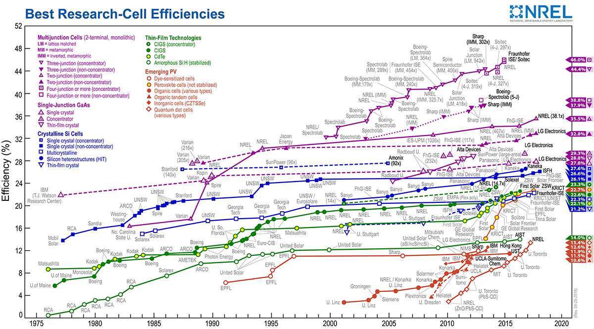
National Center for Photovoltaics (NCPV) at the National Renewable Energy Laboratory (NREL); www.nrel.gov/pv/assets/images/efficiency-chart.png
Tavakoli MM, Zakeeruddin SM, Grätzel M, Fan Z (2018) Large-grain tin-rich perovskite films for efficient solar cells via metal alloying technique. Adv Mater 30(11):1705998
Tavakoli MM, Tsui KH, Zhang Q, He J, Yao Y, Li D, Fan Z (2015) Highly efficient flexible perovskite solar cells with antireflection and self-cleaning nanostructures. ACS Nano 9(10):10287–10295
Leung SF, Tsui KH, Lin Q, Huang H, Lu L, Shieh JM, Shen CH, Hsu CH, Zhang Q, Li D, Fan Z (2014) Large scale, flexible and three-dimensional quasi-ordered aluminum nanospikes for thin film photovoltaics with omnidirectional light trapping and optimized electrical design. Energy Environ Sci 7(11):3611–3616
Hua B, Lin Q, Zhang Q, Fan Z (2013) Efficient photon management with nanostructures for photovoltaics. Nanoscale 5(15):6627–6640
Lin Y, Xu Z, Yu D, Lu L, Yin M, Tavakoli MM, Chen X, Hao Y, Fan Z, Cui Y, Li D (2016) Dual-layer nanostructured flexible thin-film amorphous silicon solar cells with enhanced light harvesting and photoelectric conversion efficiency. ACS Appl Mater Interfaces 8(17):10929–10936
Lin Q, Lu L, Tavakoli MM, Zhang C, Lui GC, Chen Z, Chen X, Tang L, Zhang D, Lin Y, Chang P (2016) High performance thin film solar cells on plastic substrates with nanostructure-enhanced flexibility. Nano Energy 22:539–547
Wang X, Li Z, Xu W, Kulkarni SA, Batabyal SK, Zhang S, Cao A, Wong LH (2015) TiO2 nanotube arrays based flexible perovskite solar cells with transparent carbon nanotube electrode. Nano Energy 11:728–735
Tavakoli MM, Lin Q, Leung SF, Lui GC, Lu H, Li L, Xiang B, Fan Z (2016) Efficient, flexible and mechanically robust perovskite solar cells on inverted nanocone plastic substrates. Nanoscale 8(7):4276–4283
Author information
Authors and Affiliations
Corresponding author
Editor information
Editors and Affiliations
Rights and permissions
Copyright information
© 2021 National Technology & Engineering Solutions of Sandia, LLC
About this chapter

Cite this chapter
Tavakoli, M.M. (2021). Efficient Light Harvesting in the Nanotextured Thin Film Solar Cells. In: Alston, M., Lambert, T.N. (eds) Energy-Sustainable Advanced Materials. Springer, Cham. https://doi.org/10.1007/978-3-030-57492-5_5
Download citation
DOI: https://doi.org/10.1007/978-3-030-57492-5_5
Published:
Publisher Name: Springer, Cham
Print ISBN: 978-3-030-57491-8
Online ISBN: 978-3-030-57492-5
eBook Packages: Chemistry and Materials ScienceChemistry and Material Science (R0)