
Abstract
This chapter introduces a group of combinational logic building blocks that are commonly used in digital design. As we move into systems that are larger than individual gates, there are naming conventions that are used to describe the size of the logic. Table 6.1 gives these naming conventions. In this chapter we will look at medium-scale integrated circuit (MSI) logic. Each of these building blocks can be implemented using the combinational logic design steps covered in Chaps. 4 and 5. The goal of this chapter is to provide an understanding of the basic principles of MSI logic.
Access provided by Autonomous University of Puebla. Download chapter PDF
This chapter introduces a group of combinational logic building blocks that are commonly used in digital design. As we move into systems that are larger than individual gates, there are naming conventions that are used to describe the size of the logic. Table 6.1 gives these naming conventions. In this chapter we will look at medium-scale integrated circuit (MSI) logic. Each of these building blocks can be implemented using the combinational logic design steps covered in Chaps. 4 and 5. The goal of this chapter is to provide an understanding of the basic principles of MSI logic.
-
6.1
Design a decoder circuit using both the classical digital design approach and the modern HDL-based approach.
-
6.2
Design an encoder circuit using both the classical digital design approach and the modern HDL-based approach.
-
6.3
Design a multiplexer circuit using both the classical digital design approach and the modern HDL-based approach.
-
6.4
Design a demultiplexer circuit using both the classical digital design approach and the modern HDL-based approach.
6.1 Decoders
A decoder is a circuit that takes in a binary code and has outputs that are asserted for specific values of that code. The code can be of any type or size (e.g., unsigned, two’s complement, etc.). Each output will assert for only specific input codes. Since combinational logic circuits only produce a single output, this means that within a decoder, there will be a separate combinational logic circuit for each output.
6.1.1 Example: One-Hot Decoder
A one-hot decoder is a circuit that has n inputs and 2n outputs. Each output will assert for one and only one input code. Since there are 2n outputs, there will always be one and only one output asserted at any given time. Example 6.1 shows the process of designing a 2-to-4 one-hot decoder by hand (i.e., using the classical digital design approach).

2-to-4 one-hot decoder – logic synthesis by hand
As decoders get larger, it is necessary to use hardware description languages to model their behavior. Example 6.2 shows how to model a 3-to-8 one-hot decoder in VHDL with concurrent signal assignments and logic operators.

3-to-8 one-hot decoder – VHDL modeling using logical operators
This description can be further simplified by using vector notation for the ports and describing the functionality using either conditional or select signal assignment. Example 6.3 shows how to model the 3-to-8 one-hot decoder in VHDL with conditional and select signal assignments.

3-to-8 one-hot decoder – VHDL modeling using conditional and select signal assignments
6.1.2 Example: 7-Segment Display Decoder
A 7-segment display decoder is a circuit used to drive character displays that are commonly found in applications such as digital clocks and household appliances. A character display is made up of seven individual LEDs, typically labeled a–g. The input to the decoder is the binary equivalent of the decimal or hex character that is to be displayed. The output of the decoder is the arrangement of LEDs that will form the character. Decoders with two inputs can drive characters “0” to “3.” Decoders with three inputs can drive characters “0” to “7.” Decoders with four inputs can drive characters “0” to “F” with the case of the hex characters being “A, b, c or C, d, E, and F.”
Let’s look at an example of how to design a 3-input, 7-segment decoder by hand. The first step in the process is to create the truth table for the outputs that will drive the LEDs in the display. We’ll call these outputs Fa, Fb, …, Fg. Example 6.4 shows how to construct the truth table for the 7-segment display decoder. In this table, a logic 1 corresponds to the LED being ON.

7-segment display decoder – truth table
If we wish to design this decoder by hand, we need to create seven separate combinational logic circuits. Each of the outputs (Fa – Fg) can be put into a 3-input K-map to find the minimized logic expression. Example 6.5 shows the design of the decoder from the truth table in Example 6.4 by hand.

7-segment display decoder – logic synthesis by hand
This same functionality can be modeled in VHDL using concurrent signal assignments with logical operators. Example 6.6 shows how to model the 7-segment decoder in VHDL using concurrent signal assignments with logic operators.

7-segment display decoder – modeling using logical operators
Again, a more compact description of the decoder can be accomplished if the ports are described as vectors and a conditional or select signal assignment is used. Example 6.7 shows how to model the 7-segment decoder in VHDL using conditional and selected signal assignments.

7-segment display decoder – modeling using conditional and selected signal assignments
Concept Check
CC6.1 In a decoder, a logic expression is created for each output. Once all of the output logic expressions are found, how can the decoder logic be further minimized?
-
A)
By using K-maps to find the output logic expressions.
-
B)
By buffering the inputs so that they can drive a large number of other gates.
-
C)
By identifying any logic terms that are used in multiple locations (inversions, product terms, and sum terms) and sharing the interim results among multiple circuits in the decoder.
-
D)
By ignoring fan-out.
6.2 Encoders
An encoder works in the opposite manner as a decoder. An assertion on a specific input port corresponds to a unique code on the output port.
6.2.1 Example: One-Hot Binary Encoder
A one-hot binary encoder has n outputs and 2n inputs. The output will be an n-bit, binary code which corresponds to an assertion on one and only one of the inputs. Example 6.8 shows the process of designing a 4-to-2 binary encoder by hand (i.e., using the classical digital design approach).

4-to-2 binary encoder – logic synthesis by hand
In VHDL this can be implemented using logical operators, conditional signal assignments, or selected signal assignments. In the conditional and selected signal assignments, if an output is not listed for each and every input possibility, then an output must be specified to cover any remaining inputs conditions. In the conditional signal assignment, the covering value is specified after the final else statement. In the selected signal assignment, the covering value is specified using the when others clause. Example 6.9 shows how to model the encoder in VHDL using each of the abovementioned modeling techniques.

4-to-2 binary encoder – VHDL modeling
Concept Check
CC6.2 If it is desired to have the outputs of an encoder produce 0’s for all input codes not defined in the truth table, can “don’t cares” be used when deriving the minimized logic expressions? Why?
-
A)
No. Don’t cares aren’t used in encoders.
-
B)
Yes. Don’t cares can always be used in K-maps.
-
C)
Yes. All that needs to be done is to treat each X as a 0 when forming the most minimal prime implicant.
-
D)
No. Each cell in the K-map corresponding to an undefined input code needs to contain a 0 so don’t cares are not applicable.
6.3 Multiplexers
A multiplexer is a circuit that passes one of its multiple inputs to a single output based on a select input. This can be thought of as a digital switch. The multiplexer has n select lines, 2n inputs, and one output. Example 6.10 shows the process of designing a 2-to-1 multiplexer by hand (i.e., using the classical digital design approach).

2-to-1 multiplexer – logic synthesis by hand
Again, in VHDL a multiplexer can be implemented using different behavioral models. Let’s look at the modeling of a 4-to-1 multiplexer in VHDL using logical operators, conditional signal assignments, and selected signal assignments. This multiplexer requires two select lines to address each of the four input lines. Each of the product terms in the multiplexer logic expression must include both select lines. The polarity of the select lines is chosen so that when an input is selected, its product term will allow the input to pass to the OR gate. In the VHDL implementation of the multiplexer using conditional and selected signal assignments, since every possible value of Sel is listed, it is not necessary to use a final else or when others clause. Example 6.11 shows the VHDL modeling of a 4-to-1 multiplexer.

4-to-1 multiplexer – VHDL modeling
Concept Check
CC6.3 How are the product terms in a multiplexer based on the identity theorem?
-
A)
Only the select product term will pass its input to the final sum term. Since all of the unselected product terms output 0, the input will be passed through the sum term because anything OR’d with a 0 is itself.
-
B)
The select lines are complemented such that they activate only one OR gate.
-
C)
The select line inputs will produce 1’s on the inputs of the selected product term. This allows the input signal to pass through the selected AND gate because anything AND’d with a 1 is itself.
-
D)
The select line inputs will produce 0’s on the inputs of the selected sum term. This allows the input signal to pass through the selected OR gate because anything OR’d with a 0 is itself.
6.4 Demultiplexers
A demultiplexer works in a complementary fashion to a multiplexer. A demultiplexer has one input that is routed to one of its multiple outputs. The output that is active is dictated by a select input. A demux has n select lines that chooses to route the input to one of its 2n outputs. When an output is not selected, it outputs a logic 0. Example 6.12 shows the process of designing a 1-to-2 demultiplexer by hand (i.e., using the classical digital design approach).

1-to-2 demultiplexer – logic synthesis by hand
Again, in VHDL a demultiplexer can be implemented using different behavioral models. Example 6.13 shows the modeling of a 1-to-4 demultiplexer in VHDL using logical operators, conditional signal assignments, and selected signal assignments. This demultiplexer requires two select lines in order to choose between the four outputs.

1-to-4 demultiplexer – VHDL modeling
Concept Check
CC6.4 How many select lines are needed in a 1-to-64 demultiplexer?
-
A)
1 B) 4 C) 6 D) 64
Summary
-
The term medium-scale integrated circuit (MSI) logic refers to a set of basic combinational logic circuits that implement simple, commonly used functions such as decoders, encoders, multiplexers, and demultiplexers. MSI logic can also include operations such as comparators and simple arithmetic circuits.
-
While an MSI logic circuit may have multiple outputs, each output requires its own unique logic expression that is based on the system inputs.
-
A decoder is a system that has a greater number of outputs than inputs. The behavior of each output is based on each unique input code.
-
An encoder is a system that has a greater number of inputs than outputs. A compressed output code is produced based on which input(s) lines are asserted.
-
A multiplexer is a system that has one output and multiple inputs. At any given time, one and only one input is routed to the output based on the value on a set of select lines. For n select lines, a multiplexer can support 2n inputs.
-
A demultiplexer is a system that has one input and multiple outputs. The input is routed to one of the outputs depending on the value on a set of select lines. For n select lines, a demultiplexer can support 2n outputs.
-
HDLs are particularly useful for describing MSI logic due to their abstract modeling capability. Through the use of Boolean conditions and vector assignments, the behavior of MSI logic can be modeled in a compact and intuitive manner.
Exercise Problems
Section 6.1: Decoders
-
6.1.1
Design a 4-to-16 one-hot decoder by hand. The block diagram and truth table for the decoder are given in Fig. 6.1. Give the minimized logic expressions for each output (i.e., F0, F1, …, F15) and the full logic diagram for the system.
Fig. 6.1 
4-to-16 one-hot decoder functionality

-
6.1.2
Design a VHDL model for a 4-to-16 one-hot decoder using concurrent signal assignments and logical operators. Use the entity definition given in Fig. 6.2.
Fig. 6.2 
4-to-16 one-hot decoder entity

-
6.1.3
Design a VHDL model for a 4-to-16 one-hot decoder using conditional signal assignments. Use the entity definition given in Fig. 6.2.
-
6.1.4
Design a VHDL model for a 4-to-16 one-hot decoder using selected signal assignments. Use the entity definition given in Fig. 6.2.
-
6.1.5
Design a 4-input, 7-segment hex character decoder by hand. The system has four inputs called A, B, C, and D. The system has seven outputs called Fa, Fb, Fc, Fd, Fe, Ff, and Fg. These outputs drive the individual LEDs within the display. A logic 1 on an output corresponds to the LED being ON. The display will show the hex characters 0–9, A, b, c, d, E, and F corresponding to the 4-bit input code on A. A template for creating the truth tables for this system is provided in Fig. 6.3. Provide the minimized logic expressions for each of the seven outputs and the overall logic diagram for the decoder.

7-segment display decoder truth table
-
6.1.6
Design a VHDL model for a 4-input, 7-segment hex character decoder using conditional signal assignments. Use the entity definition given in Fig. 6.4 for your design. The system has a 4-bit input vector called A and a 7-bit output vector called F. The individual scalars within the output vector (i.e., F(6 downto 0)) correspond to the character display segments a, b, c, d, e, f, and g, respectively. A logic 1 on an output corresponds to the LED being ON. The display will show the hex characters 0–9, A, b, c, d, E, and F corresponding to the 4-bit input code on A. A template for creating the truth table is provided in. The signals in this table correspond to the entity in this problem as follows: A = A(3), B = A(2), C = A(1), D = A(0), Fa = F(6), Fb = F(5), Fc = F(4), Fd = F(3), Fe = F(2), Ff = F(1), and Fg = F(0).
Fig. 6.4 
7-segment display decoder entity

-
6.1.7
Design a VHDL model for a 4-input, 7-segment hex character decoder using selected signal assignments. Use the entity definition given in Fig. 6.4 for your design. The system has a 4-bit input vector called A and a 7-bit output vector called F. The individual scalars within the output vector (i.e., F(6 downto 0)) correspond to the character display segments a, b, c, d, e, f, and g, respectively. A logic 1 on an output corresponds to the LED being ON. The display will show the hex characters 0–9, A, b, c, d, E, and F corresponding to the 4-bit input code on A. A template for creating the truth table for this system is provided in. The signals in this table correspond to the entity in this problem as follows: A = A(3), B = A(2), C = A(1), D = A(0), Fa = F(6), Fb = F(5), Fc = F(4), Fd = F(3), Fe = F(2), Ff = F(1), and Fg = F(0).
Section 6.2: Encoders
-
6.2.1
Design an 8-to-3 binary encoder by hand. The block diagram and truth table for the encoder are given in Fig. 6.5. Give the logic expressions for each output and the full logic diagram for the system.
Fig. 6.5 
8-to-3 one-hot encoder functionality

-
6.2.2
Design a VHDL model for an 8-to-3 binary encoder using concurrent signal assignments and logical operators. Use the entity definition given in Fig. 6.6 for your design.
Fig. 6.6 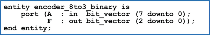
8-to-3 one-hot encoder entity

-
6.2.3
Design a VHDL model for an 8-to-3 binary encoder using conditional signal assignments. Use the entity definition given in Fig. 6.6 for your design.
-
6.2.4
Design a VHDL model for an 8-to-3 binary encoder using selected signal assignments. Use the entity definition given in Fig. 6.6 for your design.
Section 6.3: Multiplexers
-
6.3.1
Design an 8-to-1 multiplexer by hand. The block diagram and truth table for the multiplexer are given in Fig. 6.7. Give the minimized logic expressions for the output and the full logic diagram for the system.
Fig. 6.7 
8-to1 multiplexer functionality

-
6.3.2
Design a VHDL model for an 8-to-1 multiplexer using concurrent signal assignments and logical operators. Use the entity definition given in Fig. 6.8 for your design.
Fig. 6.8 
8-to1 multiplexer entity

-
6.3.3
Design a VHDL model for an 8-to-1 multiplexer using conditional signal assignments. Use the entity definition given in Fig. 6.8 for your design.
-
6.3.4
Design a VHDL model for an 8-to-1 multiplexer using selected signal assignments. Use the entity definition given in Fig. 6.8 for your design.
Section 6.4: Demultiplexers
-
6.4.1
Design a 1-to-8 demultiplexer by hand. The block diagram and truth table for the demultiplexer are given in Fig. 6.9. Give the minimized logic expressions for each output and the full logic diagram for the system.
Fig. 6.9 
1-to-8 demultiplexer functionality

-
6.4.2
Design a VHDL model for a 1-to-8 demultiplexer using concurrent signal assignments and logical operators. Use the entity definition given in Fig. 6.10 for your design.
Fig. 6.10 
1-to-8 demultiplexer entity

-
6.4.3
Design a VHDL model for a 1-to-8 demultiplexer using conditional signal assignments. Use the entity definition given in Fig. 6.10 for your design.
-
6.4.4
Design a VHDL model for a 1-to-8 demultiplexer using selected signal assignments. Use the entity definition given in Fig. 6.10 for your design.
Author information
Authors and Affiliations
Rights and permissions
Copyright information
© 2019 Springer Nature Switzerland AG
About this chapter

Cite this chapter
LaMeres, B.J. (2019). MSI Logic. In: Introduction to Logic Circuits & Logic Design with VHDL . Springer, Cham. https://doi.org/10.1007/978-3-030-12489-2_6
Download citation
DOI: https://doi.org/10.1007/978-3-030-12489-2_6
Published:
Publisher Name: Springer, Cham
Print ISBN: 978-3-030-12488-5
Online ISBN: 978-3-030-12489-2
eBook Packages: EngineeringEngineering (R0)