
Abstract
Now we turn our attention to the physical circuitry and electrical quantities that are used to represent and operate on the binary codes 1 and 0. In this chapter we begin by looking at how logic circuits are described and introduce the basic set of gates used for all digital logic operations. We then look at the underlying circuitry that implements the basic gates including digital signaling and how voltages are used to represent 1’s and 0’s. We then look at interfacing between two digital circuits and how to ensure that when one circuit sends a binary code, the receiving circuit is able to determine which code was sent. Logic families are then introduced, and the details of how basic gates are implemented at the switch level are presented. Finally, interfacing considerations are covered for the most common types of digital loads (i.e., other gates, resistors, and LEDs). The goal of this chapter is to provide an understanding of the basic electrical operation of digital circuits.
Access provided by Autonomous University of Puebla. Download chapter PDF
Now we turn our attention to the physical circuitry and electrical quantities that are used to represent and operate on the binary codes 1 and 0. In this chapter we begin by looking at how logic circuits are described and introduce the basic set of gates used for all digital logic operations. We then look at the underlying circuitry that implements the basic gates including digital signaling and how voltages are used to represent 1’s and 0’s. We then look at interfacing between two digital circuits and how to ensure that when one circuit sends a binary code, the receiving circuit is able to determine which code was sent. Logic families are then introduced, and the details of how basic gates are implemented at the switch level are presented. Finally, interfacing considerations are covered for the most common types of digital loads (i.e., other gates, resistors, and LEDs). The goal of this chapter is to provide an understanding of the basic electrical operation of digital circuits.
-
3.1
Describe the functional operation of a basic logic gate using truth tables, logic expressions, and logic waveforms.
-
3.2
Analyze the DC and AC behavior of a digital circuit to verify it is operating within specification.
-
3.3
Describe the meaning of a logic family and the operation of the most common technologies used today.
-
3.4
Determine the operating conditions of a logic circuit when driving various types of loads.
3.1 Basic Gates
The term gate is used to describe a digital circuit that implements the most basic functions possible within the binary system. When discussing the operation of a logic gate, we ignore the details of how the 1’s and 0’s are represented with voltages and manipulated using transistors. We instead treat the inputs and output as simply ideal 1’s and 0’s. This allows us to design more complex logic circuits without going into the details of the underlying physical hardware.
3.1.1 Describing the Operation of a Logic Circuit
3.1.1.1 The Logic Symbol
A logic symbol is a graphical representation of the circuit that can be used in a schematic to show how circuits in a system interface to one another. For the set of basic logic gates, there are uniquely shaped symbols that graphically indicate their functionality. For more complex logic circuits that are implemented with multiple basic gates, a simple rectangular symbol is used. Inputs of the logic circuit are typically shown on the left of the symbol and outputs are on the right. Fig. 3.1 shows two example logic symbols.

Example logic symbols
3.1.1.2 The Truth Table
We formally define the functionality of a logic circuit using a truth table. In a truth table, each and every possible input combination is listed, and the corresponding output of the logic circuit is given. If a logic circuit has n inputs, then it will have 2n possible input codes. The binary codes are listed in ascending order within the truth table mimicking a binary count starting at 0. By always listing the input codes in this way, we can assign a row number to each input that is the decimal equivalent of the binary input code. Row numbers can be used to simplify the notation for describing the functionality of larger circuits. Fig. 3.2 shows the formation of an example 3-input truth table.

Truth table formation
3.1.1.3 The Logic Function
A logic expression (also called a logic function), is an equation that provides the functionality of each output in the circuit as a function of the inputs. The logic operations for the basic gates are given a symbolic set of operators (e.g., +, ∙, ⊕), the details of which will be given in the next sections. The logic function describes the operations that are necessary to produce the outputs listed in the truth table. A logic function is used to describe a single output that can take on only the values 1 and 0. If a circuit contains multiple outputs, then a logic function is needed for each output. The input variables can be included in the expression description just as in an analog function. For example, “F (A,B,C)= …” would state that “F is a function of the inputs A, B, and C.” This can also be written as “FA,B,C = … .” The input variables can also be excluded for brevity as in “F = … .” Fig. 3.3 shows the formation of an example 3-input logic expression.

Logic function formation
3.1.1.4 The Logic Waveform
A logic waveform is a graphical depiction of the relationship of the output to the inputs with respect to time. This is often a useful description of behavior since it mimics the format that is typically observed when measuring a real digital circuit using test equipment such as an oscilloscope. In the waveform, each signal can only take on a value of 1 or 0. It is useful to write the logic values of the signal at each transition in the waveform for readability. Fig. 3.4 shows an example logic waveform.

Example logic waveform
3.1.2 The Buffer
The first basic gate is the buffer. The output of a buffer is simply the input. The logic symbol, truth table, logic function, and logic waveform for the buffer are given in Fig. 3.5.

Buffer symbol, truth table, logic function, and logic waveform
3.1.3 The Inverter
The next basic gate is the inverter. The output of an inverter is the complement of the input. Inversion is also often called the not operation. In spoken word, we might say “A is equal to not B”; thus this gate is also often called a not gate. The symbol for the inverter is the same as the buffer with the exception that an inversion bubble (i.e., a circle) is placed on the output. The inversion bubble is a common way to show inversions in schematics and will be used by many of the basic gates. In the logic function, there are two common ways to show this operation. The first way is by placing a prime (‘) after the input variable (e.g., Out = In’). This notation has the advantage that it is supported in all text editors but has the drawback that it can sometimes be difficult to see. The second way to indicate inversion in a logic function is by placing an inversion bar over the input variable (e.g., Out = ). The advantage of this notation is that it is easy to see but has the drawback that it is not supported by many text editors. In this text, both conventions will be used to provide exposure to each. The logic symbol, truth table, logic function, and logic waveform for the inverter are given in Fig. 3.6.

Inverter symbol, truth table, logic function, and logic waveform
3.1.4 The AND Gate
The next basic gate is the AND gate. The output of an AND gate will only be true (i.e., a logic 1) if all of the inputs are true. This operation is also called a logical product because if the inputs were multiplied together, the only time the output would be a 1 is if each and every input was a 1. As a result, the logic operator is the dot (∙). Another notation that is often seen is the ampersand (&). The logic symbol, truth table, logic function, and logic waveform for a 2-input AND gate are given in Fig. 3.7.

Input AND gate symbol, truth table, logic function, and logic waveform
Ideal AND gates can have any number of inputs. The operation of an n-bit, AND gates still follows the rule that the output will only be true when all of the inputs are true. Later sections will discuss the limitations on expanding the number of inputs of these basic gates indefinitely.
3.1.5 The NAND Gate
The NAND gate is identical to the AND gate with the exception that the output is inverted. The “N” in NAND stands for “NOT,” which represents the inversion. The symbol for a NAND gate is an AND gate with an inversion bubble on the output. The logic expression for a NAND gate is the same as an AND gate but with an inversion bar over the entire operation. The logic symbol, truth table, logic function, and logic waveform for a 2-input NAND gate are given in Fig. 3.8. Ideal NAND gates can have any number of inputs with the operation of an n-bit, NAND gate following the rule that the output is always the inversion of an n-bit, AND operation.

Input NAND gate symbol, truth table, logic function, and logic waveform
3.1.6 The OR Gate
The next basic gate is the OR gate. The output of an OR gate will be true when any of the inputs are true. This operation is also called a logical sum because of its similarity to logical disjunction in which the output is true if at least one of the inputs is true. As a result, the logic operator is the plus sign (+). The logic symbol, truth table, logic function, and logic waveform for a 2-input OR gate are given in Fig. 3.9. Ideal OR gates can have any number of inputs. The operation of an n-bit, OR gates still follows the rule that the output will be true if any of the inputs are true.

Input OR gate symbol, truth table, logic function, and logic waveform
3.1.7 The NOR Gate
The NOR gate is identical to the OR gate with the exception that the output is inverted. The symbol for a NOR gate is an OR gate with an inversion bubble on the output. The logic expression for a NOR gate is the same as an OR gate but with an inversion bar over the entire operation. The logic symbol, truth table, logic function, and logic waveform for a 2-input NOR gate are given in Fig. 3.10. Ideal NOR gates can have any number of inputs with the operation of an n-bit, NOR gate following the rule that the output is always the inversion of an n-bit, OR operation.

Input NOR gate symbol, truth table, logic function, and logic waveform
3.1.8 The XOR Gate
The next basic gate is the exclusive-OR gate, or XOR gate for short. This gate is also called a difference gate because for the 2-input configuration, its output will be true when the input codes are different from one another. The logic operator is a circle around a plus sign (⊕). The logic symbol, truth table, logic function, and logic waveform for a 2-input XOR gate are given in Fig. 3.11.

Input XOR gate symbol, truth table, logic function, and logic waveform
Using the formal definition of an XOR gate (i.e., the output is true if any of the input codes are different from one another), an XOR gate with more than two inputs can be built. The truth table for a 3-bit, XOR gate using this definition is shown in Fig. 3.12. In modern electronics, this type of gate has found little use since it is much simpler to build this functionality using a combination of AND and OR gates. As such, XOR gates with greater than two inputs do not implement the difference function. Instead, a more useful functionality has been adopted in which the output of the n-bit, XOR gate is the result of a cascade of 2-input XOR gates. This results in an ultimate output that is true when there is an ODD number of 1’s on the inputs. This functionality is much more useful in modern electronics for error correction codes and arithmetic. As such, this is the functionality that is seen in modern n-bit, XOR gates. This functionality is also shown in Fig. 3.12.

Input XOR gate implementation
3.1.9 The XNOR Gate
The exclusive-NOR gate is identical to the XOR gate with the exception that the output is inverted. This gate is also called an equivalence gate because for the 2-input configuration, its output will be true when the input codes are equivalent to one another. The symbol for an XNOR gate is an XOR gate with an inversion bubble on the output. The logic expression for an XNOR gate is the same as an XOR gate but with an inversion bar over the entire operation. The logic symbol, truth table, logic function, and logic waveform for a 2-input XNOR gate are given in Fig. 3.13. XNOR gates can have any number of inputs with the operation of an n-bit, XNOR gate following the rule that the output is always the inversion of an n-bit, XOR operation (i.e., the output is true if there is an ODD number of 1’s on the inputs).

Input XNOR gate symbol, truth table, logic function, and logic waveform
Concept Check
CC3.1 Given the following logic diagram, which is the correct logic expression for F?

-
A)
F = (A·B)’ ⊕ C
-
B)
F = (A’·B’) ⊕ C
-
C)
F = (A’·B’ ⊕ C)
-
D)
F = A·B’ ⊕ C
3.2 Digital Circuit Operation
Now we turn our attention to the physical hardware that is used to build the basic gates just described and how electrical quantities are used to represent and communicate the binary values 1 and 0. We begin by looking at digital signaling. Digital signaling refers to how binary codes are generated and transmitted successfully between two digital circuits using electrical quantities (e.g., voltage and current). Consider the digital system shown in Fig. 3.14. In this system, the sending circuit generates a binary code. The sending circuit is called either the transmitter (Tx) or driver. The transmitter represents the binary code using an electrical quantity such as voltage. The receiving circuit (Rx) observes this voltage and is able to determine the value of the binary code. In this way, 1’s and 0’s can be communicated between the two digital circuits. The transmitter and receiver are both designed to use the same digital signaling scheme so that they are able to communicate with each other. It should be noted that all digital circuits contain both inputs (Rx) and outputs (Tx) but are not shown in this figure for simplicity.

Generic digital transmitter/receiver circuit
3.2.1 Logic Levels
A logic level is the term to describe all possible states that a signal can have. We will focus explicitly on circuits that represent binary values, so these will only have two finite states (1 and 0). To begin, we define a simplistic model of how to represent the binary codes using an electrical quantity. This model uses a voltage threshold (Vth) to represent the switching point between the binary codes. If the voltage of the signal (Vsig) is above this threshold, it is considered a logic HIGH. If the voltage is below this threshold, it is considered a logic LOW. A graphical depiction of this is shown in Fig. 3.15. The terms HIGH and LOW are used to describe which logic level corresponds to the higher or lower voltage.

Definition of logic HIGH and LOW
It is straightforward to have the HIGH level correspond to the binary code 1 and the LOW level correspond to the binary code 0; however, it is equally valid to have the HIGH level correspond to the binary code 0 and the LOW level correspond to the binary code 1. As such, we need to define how the logic levels HIGH and LOW map to the binary codes 1 and 0. We define two types of digital assignments: positive logic and negative logic. In positive logic, the logic HIGH level represents a binary 1, and the logic LOW level represents a binary 0. In negative logic, the logic HIGH level represents a binary 0, and the logic LOW level represents a binary 1. Table 3.1 shows the definition of positive and negative logic. There are certain types of digital circuits that benefit from using negative logic; however, we will focus specifically on systems that use positive logic since it is more intuitive when learning digital design for the first time. The transformation between positive and negative logic is straightforward and will be covered in Chap. 4.
3.2.2 Output DC Specifications
Transmitting circuits provide specifications on the range of output voltages (VO) that they are guaranteed to provide when outputting a logic 1 or 0. These are called the DC output specifications. There are four DC voltage specifications that specify this range: VOH−max, VOH−min, VOL−max, and VOL−-min. The VOH−max and VOH−min specifications provide the range of voltages the transmitter is guaranteed to provide when outputting a logic HIGH (or logic 1 when using positive logic). The VOL−max and VOL−min specifications provide the range of voltages the transmitter is guaranteed to provide when outputting a logic LOW (or logic 0 when using positive logic). In the subscripts for these specifications, the “O” signifies “output,” and the “L” or “H” signifies “LOW” or “HIGH,” respectively.
The maximum amount of current that can flow through the transmitter’s output (IO) is also specified. The specification IOH−max is the maximum amount of current that can flow through the transmitter’s output when sending a logic HIGH. The specification IOL−max is the maximum amount of current that can flow through the transmitter’s output when sending a logic LOW. When the maximum output currents are violated, it usually damages the part. Manufacturers will also provide a recommended amount of current for IO that will guarantee the specified operating parameters throughout the life of the part. Figure 3.16 shows a graphical depiction of these DC specifications. When the transmitter output is providing current to the receiving circuit (a.k.a., the load), it is said to be sourcing current. When the transmitter output is drawing current from the receiving circuit, it is said to be sinking current. In most cases, the transmitter sources current when driving a logic HIGH and sinks current when driving a logic LOW. Fig. 3.16 shows a graphical depiction of these specifications.

DC specifications of a digital circuit
3.2.3 Input DC Specifications
Receiving circuits provide specifications on the range of input voltages (VI) that they will interpret as either a logic HIGH or LOW. These are called the DC input specifications. There are four DC voltage specifications that specify this range: VIH−max, VIH−min, VIL−max, and VIL−min. The VIH−max and VIH−min specifications provide the range of voltages that the receiver will interpret as a logic HIGH (or logic 1 when using positive logic). The VIL−max and VIL−min specifications provide the range of voltages that the receiver will interpret as a logic LOW (or logic 0 when using positive logic). In the subscripts for these specifications, the “I” signifies “input.”
The maximum amount of current that the receiver will draw, or take in, when connected is also specified II). The specification IIH−max is the maximum amount of current that the receiver will draw when it is being driven with a logic HIGH. The specification IIL−max is the maximum amount of current that the receiver will draw when it is being driven with a logic LOW. Again, Fig. 3.16 shows a graphical depiction of these DC specifications.
3.2.4 Noise Margins
For digital circuits that are designed to operate with each other, the VOH−max and VIH−max specifications have equal voltages. Similarly, the VOL−min and VIL−min specifications have equal voltages. The VOH−max and VOL−min output specifications represent the best-case scenario for digital signaling as the transmitter is sending the largest (or smallest) signal possible. If there is no loss in the interconnect between the transmitter and receiver, the full voltage levels will arrive at the receiver and be interpreted as the correct logic states (HIGH or LOW).
The worst-case scenario for digital signaling is when the transmitter outputs its levels at VOH−min and VOL−max. These levels represent the furthest away from an ideal voltage level that the transmitter can send to the receiver and are susceptible to loss and noise that may occur in the interconnect system. In order to compensate for potential loss or noise, digital circuits have a pre-defined amount of margin built into their worst-case specifications. Let’s take the worst-case example of a transmitter sending a logic HIGH at the level VOH−min. If the receiver was designed to have VIH−min (i.e., the lowest voltage that would still be interpreted as a logic 1) equal to VOH−min, then if even the smallest amount of the output signal was attenuated as it traveled through the interconnect, it would arrive at the receiver below VIH−min and would not be interpreted as a logic 1. Since there will always be some amount of loss in any interconnect system, the specifications for VIH−min are always less than VOH−min. The difference between these two quantities is called the noise margin. More specifically, it is called the noise margin HIGH (or NMH) to signify how much margin is built into the Tx/Rx circuit when communicating a logic 1. Similarly, the VIL−max specification is always higher than the VOL−max specification to account for any voltage added to the signal in the interconnect. The difference between these two quantities is called the noise margin LOW (or NML) to signify how much margin is built into the Tx/Rx circuit when communicating a logic 0. Noise margins are always specified as positive quantities, thus the order of the subtrahend and minuend in these differences.
Figure 3.16 includes the graphical depiction of the noise margins. Notice in this figure that there is a region of voltages that the receiver will not interpret as either a HIGH or LOW. This region lies between the VIH−min and VIL−max specifications. This is the uncertainty region and should be avoided. Signals in this region will cause the receiver’s output to go to an unknown voltage. Digital transmitters are designed to transition between the LOW and HIGH states quickly enough so that the receiver does not have time to react to the input being in the uncertainty region.
3.2.5 Power Supplies
All digital circuits require a power supply voltage and a ground. There are some types of digital circuits that may require multiple power supplies. For simplicity, we will focus on digital circuits that only require a single power supply voltage and ground. The power supply voltage is commonly given the abbreviations of either VCC or VDD. The “CC” or “DD” have to do with how the terminals of the transistors inside of the digital circuit are connected (i.e., “collector to collector” or “drain to drain”). Digital circuits will specify the required power supply voltage. Ground is considered an ideal 0v. Digital circuits will also specify the maximum amount of DC current that can flow through the VCC (ICC) and GND (IGND) pins before damaging the part.
There are two components of power supply current. The first is the current that is required for the functional operation of the device. This is called the quiescent current (Iq). The second component of the power supply current is the output currents (IO). Any current that flows out of a digital circuit must also flow into it. When a transmitting circuit sources current to a load on its output pin, it must bring in that same amount of current on another pin. This is accomplished using the power supply pin (VCC). Conversely, when a transmitting circuit sinks current from a load on its output pin, an equal amount of current must exit the circuit on a different pin. This is accomplished using the GND pin. This means that the amount of current flowing through the VCC and GND pins will vary depending on the logic states that are being driven on the outputs. Since a digital circuit may contain numerous output pins, the maximum amount of current flowing through the VCC and GND pins can scale quickly and care must be taken not to damage the device.
The quiescent current is often specified using the term ICC. This should not be confused with the specification for the maximum amount of current that can flow through the VCC pin, which is often called ICC-max. It is easy to tell the difference because ICC (or Iq) is much smaller than ICC-max for CMOS parts. ICC (or Iq) is specified in the uA to nA range, while the maximum current that can flow through the VCC pin is specified in the mA range. Example 3.1 shows the process of calculating the ICC and IGND currents when sourcing multiple loads.

Calculating ICC and IGND when sourcing multiple loads
Example 3.2 shows the process of calculating the ICC and IGND currents when both sourcing and sinking loads.

Calculating ICC and IGND when both sourcing and sinking loads
3.2.6 Switching Characteristics
Switching characteristics refer to the transient behavior of the logic circuits. The first group of switching specifications characterize the propagation delay of the gate. The propagation delay is the time it takes for the output to respond to a change on the input. The propagation delay is formally defined as the time it takes from the point at which the input has transitioned to 50% of its final value to the point at which the output has transitioned to 50% of its final value. The initial and final voltages for the input are defined to be GND and VCC, while the output initial and final voltages are defined to be VOL and VOH. Specifications are given for the propagation delay when transitioning from a LOW to HIGH (tPLH) and from a HIGH to LOW (tPHL). When these specifications are equal, the values are often given as a single specification of tpd. These specifications are shown graphically in Fig. 3.17.

Switching characteristics of a digital circuit
The second group of switching specifications characterize how quickly the output switches between states. The transition time is defined as the time it takes for the output to transition from 10% to 90% of the output voltage range. The rise time (tr) is the time it takes for this transition when going from a LOW to HIGH, and the fall time (tf) is the time it takes for this transition when going from a HIGH to LOW. When these specifications are equal, the values are often given as a single specification of tt. These specifications are shown graphically in Fig. 3.17.
3.2.7 Data Sheets
The specifications for a particular part are given in its data sheet. The data sheet contains all of the operating characteristics for a part, in addition to functional information such as package geometries and pin assignments. The data sheet is usually the first place a designer will look when selecting a part. Figures 3.18, 3.19, and 3.20 show excerpts from an example data sheet highlighting some of the specifications just covered.

Example data sheet excerpt (1)

Example data sheet excerpt (2)

Example data sheet excerpt (3)
Concept Check
CC3.2(a) Given the following DC specifications for a driver/receiver pair, in what situation may a logic signal transmitted not be successfully received?
VOH-max = +3.4v | VIH-max = +3.4v |
VOH-min = +2.5v | VIH-min = +2.5v |
VOL-max = +1.5v | VIL-max = +2.0v |
VOL-min = 0v | VIL-min = 0v |
-
A)
Driving a HIGH with Vo=+3.4v
-
B)
Driving a HIGH with Vo=+2.5v
-
C)
Driving a LOW with Vo=+1.5v
-
D)
Driving a LOW with Vo=0v
CC3.2(b)For the following driver configuration, which of the following is a valid constraint that could be put in place to prevent a violation of the maximum power supply currents (ICC-max and IGND-max)?

-
A)
Modify the driver transistors so that they can’t provide more than 5mA on any output.
-
B)
Apply a cooling system (e.g., a heat sink or fan) to the driver chip.
-
C)
Design the logic so that no more than half of the outputs are HIGH at any given time.
-
D)
Drive multiple receivers with the same output pin.
CC3.2(c)Why is it desirable to have the output of a digital circuit transition quickly between the logic LOW and logic HIGH levels?
-
A)
So that the outputs are not able to respond as the input transitions through the uncertainty region. This avoids unwanted transitions.
-
B)
So that all signals look like square waves.
-
C)
To reduce power by minimizing the time spent switching.
-
D)
Because the system can only have two states, a LOW and a HIGH.
3.3 Logic Families
It is apparent from the prior discussion of operating conditions that digital circuits need to have comparable input and output specifications in order to successfully communicate with each other. If a transmitter outputs a logic HIGH as +3.4v and the receiver needs a logic HIGH to be above +4v to be successfully interpreted as a logic HIGH, then these two circuits will not be able to communicate. In order to address this interoperability issue, digital circuits are grouped into logic families. A logic family is a group of parts that all adhere to a common set of specifications so that they work together. The logic family is given a specific name, and once the specifications are agreed upon, different manufacturers produce parts that work within the particular family. Within a logic family, parts will all have the same power supply requirements and DC input/output specifications such that if connected directly, they will be able to successfully communicate with each other. The phrase “connected directly” is emphasized because it is very possible to insert an interconnect circuit between two circuits within the same logic family and alter the output voltage enough so that the receiver will not be able to interpret the correct logic level. Analyzing the effect of the interconnect circuit is part of the digital design process. There are many logic families that exist (up to 100 different types!) and more emerge each year as improvements are made to circuit fabrication processes that create smaller, faster, and lower power circuits.
3.3.1 Complementary Metal Oxide Semiconductors (CMOS)
The first group of logic families we will discuss is called complementary metal oxide semiconductors, or CMOS. This is currently the most popular group of logic families for digital circuits implemented on the same integrated circuit (IC). An integrated circuit is where the entire circuit is implemented on a single piece of semiconductor material (or chip). The IC can contain transistors, resistors, capacitors, inductors, wires, and insulators. Modern integrated circuits can contain billions of devices and meters of interconnect. The opposite of implementing the circuit on an integrated circuit is to use discrete components. Using discrete components refers to where every device (transistor, resistor, etc.) is its own part and is wired together externally using either a printed circuit board (PCB) or jumper wires as on a breadboard. The line between ICs and discrete parts has blurred in the past decades because modern discrete parts are actually fabricated as an IC and regularly contain multiple devices (e.g., 4 logic gates per chip). Regardless, the term discrete is still used to describe components that only contain a few components where the term IC typically refers to a much larger system that is custom designed.
The term CMOS comes from the use of particular types of transistors to implement the digital circuits. The transistors are created using a metal oxide semiconductor (MOS) structure. These transistors are turned on or off based on an electric field, so they are given the name metal oxide semiconductor field effect transistors or MOSFETs. There are two transistors that can be built using this approach that operate complementary to each other, thus the term complementary metal oxide semiconductors. To understand the basic operation of CMOS logic, we begin by treating the MOSFETs as ideal switches. This allows us to understand the basic functionality without diving into the detailed electronic analysis of the transistors.
3.3.1.1 CMOS Operation
In CMOS, there is a single power supply (VCC or VDD) and a single ground (GND). The ground signal is sometimes called VSS. The maximum input and output DC specifications are equal to the power supply (VCC = VOH-max = VIH-max). The minimum input and output DC specification are equal to ground (GND = 0v = VOL-min = VIL-min). In this way, using CMOS simplifies many of the specifications. If you state that you are using “CMOS with a +3.4v power supply,” you are inherently stating that VCC = VOH-max = VIH-max = +3.4v and that VOL-min = VIL-min = 0v. Many times, the name of the logic family will be associated with the power supply voltage. For example, a logic family may go by the name “+3.3v CMOS” or “+2.5v CMOS.” These names give a first-level description of the logic family operation, but more details about the operation must be looked up in the data sheet.
There are two types of transistors used in CMOS. The transistors will be closed or open based on an input logic level. The first transistor is called an N-type MOSFET, or NMOS. This transistor will turn on, or close, when the voltage between the gate and source (VGS) is greater than its threshold voltage. The threshold voltage (VT) is the amount of voltage needed to create a conduction path between the drain and the source terminals. The threshold voltage of an NMOS transistor is typically between 0.2v and 1v and much less than the VCC voltage in the system. The second transistor is called a P-type MOSFET, or PMOS. This transistor turns on, or closes, when the voltage between the gate and the source (VGS) is less than VT, where the VT for a PMOS is a negative value. This means that to turn on a PMOS transistor, the gate terminal needs to be at a lower voltage than the source. The type of transistor (i.e., P-type or N-type) has to do with the type of semiconductor material used to conduct current through the transistor. An NMOS transistor uses negative charge to conduct current (i.e., negative-type), while a PMOS uses positive charge (i.e., positive-type). Figure 3.21 shows the symbols for the PMOS and NMOS, the fabrication cross sections, and their switch-level equivalents.

CMOS transistors
The basic operation of CMOS is that when driving a logic HIGH, the switches are used to connect the output to the power supply (VCC), and when driving a logic LOW, the switches are used to connect the output to GND. In CMOS, VCC is considered an ideal logic HIGH, and GND is considered an ideal logic LOW. VCC is typically much larger than VT so using these levels can easily turn on and off the transistors. The design of the circuit must never connect the output to VCC and GND at the same time or else the device itself will be damaged due to the current flowing directly from VCC to GND through the transistors. Due to the device physics of the MOSFETS, PMOS transistors are used to form the network that will connect the output to VCC (a.k.a., the pull-up network), and NMOS transistors are used to form the network that will connect the output to GND (a.k.a., the pull-down network). Since PMOS transistors are closed when the input is a 0 (thus providing a logic HIGH on the output) and NMOS transistors are closed when the input is a 1 (thus providing a logic LOW on the output), CMOS implements negative logic gates. This means CMOS can implement inverters, NAND and NOR gates but not buffers, AND and OR gates directly. In order to create a CMOS AND gate, the circuit would implement a NAND gate followed by an inverter and similarly for an OR gate and buffer.
3.3.1.2 CMOS Inverter
Let’s now look at how we can use these transistors to create a CMOS inverter. Consider the transistor arrangement shown in Fig. 3.22.

CMOS inverter schematic
The inputs of both the PMOS and NMOS are connected together. The PMOS is used to connect the output to VCC and the NMOS is used to connect the output to GND. Since the inputs are connected together and the switches operate in a complementary manner, this circuit ensures that both transistors will never be on at the same time. When In = 0, the PMOS switch is closed, and the NMOS switch is open. This connects the output directly to VCC, thus providing a logic HIGH on the output. When In = 1, the PMOS switch is open, and the NMOS switch is closed. This connects the output directly to GND, thus providing a logic LOW. This configuration yields an inverter. This operation is shown graphically in Fig. 3.23.

CMOS inverter operation
3.3.1.3 CMOS NAND Gate
Let’s now look at how we use a similar arrangement of transistors to implement a 2-input NAND gate. Consider the transistor configuration shown in Fig. 3.24.

CMOS 2-input NAND gate schematic
The pull-down network consists of two NMOS transistors in series (M1 and M2) and the pull-up network consists of two PMOS transistors in parallel (M3 and M4). Let’s go through each of the input conditions and examine which transistors are on and which are off and how they impact the output. The first input condition is when A = 0 and B = 0. This condition turns on both M3 and M4 creating two parallel paths between the output and VCC. At the same time, it turns off both M1 and M2 preventing a path between the output and GND. This input condition results in an output that is connected to VCC resulting in a logic HIGH. The second input condition is when A = 0 and B = 1. This condition turns on M3 in the pull-up network and M2 in the pull-down network. This condition also turns off M4 in the pull-up network and M1 in the pull-down network. Since the pull-up network is a parallel combination of PMOS transistors, there is still a path between the output and VCC through M3. Since the pull-down network is a series combination of NMOS transistors, both M1 and M2 must be on in order to connect the output to GND. This input condition results in an output that is connected to VCC resulting in a logic HIGH. The third input condition is when A = 1 and B = 0. This condition again provides a path between the output and VCC through M4 and prevents a path between the output and ground by having M2 open. This input condition results in an output that is connected to VCC resulting in a logic HIGH. The final input condition is when A = 1 and B = 1. In this input condition, both of the PMOS transistors in the pull-up network (M3 and M4) are off preventing the output from being connected to VCC. At the same time, this input turns on both M1 and M2 in the pull-down network connecting the output to GND. This input condition results in an output that is connected to GND resulting in a logic LOW. Based on the resulting output values corresponding to the four input codes, this circuit yields the logic operation of a 2-input NAND gate. This operation is shown graphically in Fig. 3.25.

CMOS 2-input NAND gate operation
Creating a CMOS NAND gate with more than 2 inputs is accomplished by adding additional PMOS transistors to the pull-up network in parallel and additional NMOS transistors to the pull-down network in series. Figure 3.26 shows the schematic for a 3-input NAND gate. This procedure is followed for creating NAND gates with larger numbers of inputs.

CMOS 3-input NAND gate schematic
If the CMOS transistors were ideal switches, the approach of increasing the number of inputs could be continued indefinitely. In reality, the transistors are not ideal switches, and there is a limit on how many transistors can be added in series and continue to operate. The limitation has to do with ensuring that each transistor has enough voltage to properly turn on or off. This is a factor in the series network because the drain terminals of the NMOS transistors are not all connected to GND. If a voltage develops across one of the lower transistors (e.g., M3), then it takes more voltage on the input to turn on the next transistor up (e.g., M2). If too many transistors are added in series, then the uppermost transistor in the series may not be able to be turned on or off by the input signals. The number of inputs that a logic gate can have within a particular logic family is called its fan-in specification. When a logic circuit requires a number of inputs that exceeds the fan-in specification for a particular logic family, then additional logic gates must be used. For example, if a circuit requires a 5-input NAND gate but the logic family has a fan-in specification of 4, this means that the largest NAND gate available only has 4 inputs. The 5-input NAND operation must be accomplished using additional circuit design techniques that use gates with 4 or less inputs. These design techniques will be covered in Chap. 4.
3.3.1.4 CMOS NOR Gate
A CMOS NOR gate is created using a similar topology as a NAND gate with the exception that the pull-up network consists of PMOS transistors in series and the pull-down network that consists of NMOS transistors in parallel. Consider the transistor configuration shown in Fig. 3.27.

CMOS 2-input NOR gate schematic
The series configuration of the pull-up network will only connect the output to VCC when both inputs are 0. Conversely, the pull-down network prevents connecting the output to GND when both inputs are 0. When either or both of the inputs are true, the pull-up network is off, and the pull-down network is on. This yields the logic function for a NOR gate. This operation is shown graphically in Fig. 3.28. As with the NAND gate, the number of inputs can be increased by adding more PMOS transistors in series in the pull-up network and more NMOS transistors in parallel in the pull-down network.

CMOS 2-input NOR gate operation
The schematic for a 3-input NOR gate is given in Fig. 3.29. This approach can be used to increase the number of inputs up until the fan-in specification of the logic family is reached.

CMOS 3-input NOR gate schematic
3.3.2 Transistor-Transistor Logic (TTL)
One of the first logic families that emerged after the invention of the integrated circuit was transistor-transistor logic (TTL). This logic family uses bipolar junction transistor (BJT) as its fundamental switching item. This logic family defined a set of discrete parts that contained all of the basic gates in addition to more complex building blocks. TTL was used to build the first computer systems in the 1960s. TTL is not widely used today other than for specific applications because it consumes more power than CMOS and cannot achieve the density required for today’s computer systems. TTL is discussed because it was the original logic family based on integrated circuits, so it provides a historical perspective of digital logic. Furthermore, the discrete logic pin-outs and part-numbering schemes are still used today for discrete CMOS parts.
3.3.2.1 TTL Operation
TTL logic uses BJT transistors and resistors to accomplish the logic operations. The operation of a BJT transistor is more complicated than a MOSFET; however, it performs essentially the same switch operation when used in a digital logic circuit. An input is used to turn the transistor on, which in turn allows current to flow between two other terminals. Figure 3.30 shows the symbol for the two types of BJT transistors. The PNP transistor is analogous to a PMOS, and the NPN is analogous to an NMOS. Current will flow between the emitter and collector terminals when there is a sufficient voltage on the base terminal. The amount of current that flows between the emitter and collector is related to the current flowing into the base. The primary difference in operation between BJTs and MOSFETs is that BJTs require proper voltage biasing in order to turn on and also draws current through the BASE in order to stay on. The detailed operation of BJTs is beyond the scope of this text, so an overly simplified model of TTL logic gates is given.

PNP and NPN transistors
Figure 3.31 shows a simplified model of how TTL logic operates using BJTs and resistors. This simplified model does not show all of the transistors that are used in modern TTL circuits but instead is intended to provide a high-level overview of the operation. This gate is an inverter that is created with an NPN transistor and a resistor. When the input is a logic HIGH, the NPN transistor turns on and conducts current between its collector and emitter terminals. This in effect closes the switch and connects the output to GND providing a logic LOW. During this state, current will also flow through the resistor to GND through Q1 thus consuming more power than the equivalent gate in CMOS. When the input is a logic LOW, the NPN transistor turns off and no current flows between its collector and emitter. This, in effect, is an open circuit leaving only the resistor connected to the output. The resistor pulls the output up to VCC providing a logic HIGH on the output. One drawback of this state is that there will be a voltage drop across the resistor, so the output is not pulled fully to VCC.

TTL inverter
3.3.3 The 7400 Series Logic Families
The 7400 series of TTL circuits became popular in the 1960s and 1970s. This family was based on TTL and contained hundreds of different digital circuits. The original circuits came in either plastic or ceramic dual-in-line packages (DIP). The 7400 TTL logic family was powered off of a + 5v supply. As mentioned before, this logic family set the pin-outs and part-numbering schemes for modern logic families. There were many derivatives of the original TTL logic family that made modifications to improve speed and reliability, decrease power, and reduce power supplies. Today’s CMOS logic families within the 7400 series still use the same pin-outs and numbering schemes as the original TTL family. It is useful to understand the history of this series because these parts are often used in introductory laboratory exercises to learn how to interface digital logic circuits.
3.3.3.1 Part Numbering Scheme
The part numbering scheme for the 7400 series and its derivatives contains five different fields: (1) manufacturer, (2) temperature range, (3) logic family, (4) logic function, and (5) package type. The breakdown of these fields is shown in Fig. 3.32.

7400 series part numbering scheme
3.3.3.2 DC Operating Conditions
Table 3.2 gives the DC operating conditions for a few of the logic families within the 7400 series. Notice that the CMOS families consume much less power than the TTL families. Also notice that the TTL output currents are asymmetrical. The differences between the IOH and IOL within the TTL families have to do with the nature of the bipolar transistors, and the resistors used to create the pull-up networks within the devices. CMOS has symmetrical drive currents due to using complementary transistors for the pull-up (PMOS) and pull-down networks (NMOS).
3.3.3.3 Pin-out Information for the DIP Packages
Figure 3.33 shows the pin-out assignments for a subset of the basic gates from the 74HC logic family in the dual-in-line package form factor. Most of the basic gates within the 7400 series follow these assignments. Notice that each of these basic gates comes in a 14-pin DIP package, each with a single VCC and single GND pin. It is up to the designer to ensure that the maximum current flowing through the VCC and GND pins does not exceed the maximum specification. This is particularly important for parts that contain numerous gates. For example, the 74HC00 part contains four, 2-input NAND gates. If each of the NAND gates was driving a logic HIGH at its maximum allowable output current (i.e., 25 mA from Fig. 3.19), then a total of 4∙25 mA + Iq = ~100 mA would be flowing through its VCC pin. Since the VCC pin can only tolerate a maximum of 50 mA of current (from Fig. 3.19), the part would be damaged since the output current of ~100 mA would also flow through the VCC pin. The pin-outs in Fig. 3.33 are useful when first learning to design logic circuits because the DIP packages plug directly into a standard breadboard.

Pin-outs for a subset of basic gates from the 74HC logic family in DIP packages
Concept Check
CC3.3 Why doesn’t the following CMOS transistor configuration yield a buffer?

-
A)
In order to turn on the NMOS transistor, VGS needs to be greater than zero. In the given configuration, the gate terminal of the NMOS (G) needs to be driven above the source terminal (S). If the source terminal was at +3.4v, then the input (In) would never be able to provide a positive enough voltage to ensure the NMOS is on because “In” doesn’t go above +3.4v.
-
B)
There is no way to turn on both transistors in this configuration.
-
C)
The power consumption will damage the device because both transistors will potentially be on.
-
D)
The sources of the two devices can’t be connected together without causing a short in the device.
3.4 Driving Loads
At this point we’ve discussed in depth how proper care must be taken to ensure that not only do the output voltages of the driving gate meet the input specifications of the receiver in order to successfully transmit 1’s and 0’s, but that the output current of the driver does not exceed the maximum specifications so that the part is not damaged. The output voltage and current for a digital circuit depend greatly on the load that is being driven. The following sections discuss the impact of driving some of the most common digital loads.
3.4.1 Driving Other Gates
Within a logic family, all digital circuits are designed to operate with one another. If there is minimal loss or noise in the interconnect system, then 1’s and 0’s will be successfully transmitted, and no current specifications will be exceeded. Consider the example in Example 3.3 for an inverter driving another inverter from the same logic family.

Determining if specifications are violated when driving another gate as a load
From this example, it is clear that there are no issues when a gate is driving another gate from the same family. This is as expected because that is the point of a logic family. In fact, gates are designed to drive multiple gates from within their own family. Based solely on the DC specifications for input and output current, it could be assumed that the number of other gates that can be driven is simply IO-max/II-max. For the example in Example 3.3, this would result in a 74HC gate being able to drive 25,000 other gates (i.e., 25 mA/1uA = 25,000). In reality, the maximum number of gates that can be driven is dictated by the switching characteristics. This limit is called the fan-out specification. The fan-out specification states the maximum number of other gates from within the same family that can be driven. As discussed earlier, the output signal needs to transition quickly through the uncertainty region so that the receiver does not have time to react and go to an unknown state. As more and more gates are driven, this transition time is slowed down. The fan-out specification provides a limit to the maximum number of gates from the same family that can be driven while still ensuring that the output signal transitions between states fast enough to avoid the receivers from going to an unknown state. Example 3.4 shows the process of determining the maximum output current that a driver will need to provide when driving the maximum number of gates allowed by the fan-out specification.

Determining the output current when driving multiple gates as the load
3.4.2 Driving Resistive Loads
There are many situations where a resistor is the load in a digital circuit. A resistive load can be an actual resistor that is present for some other purpose such as a pull-up, pull-down, or for impedance matching. More complex loads such as buzzers, relays, or other electronics can also be modeled as a resistor. When a resistor is the load in a digital circuit, care must be taken to avoid violating the output current specifications of the driver. The electrical circuit analysis technique that is used to evaluate how a resistive load impacts a digital circuit is Ohm’s law. Ohm’s law is a very simple relationship between the current and voltage in a resistor. Fig. 3.34 gives a primer on Ohm’s law. For use in digital circuits, there are only a select few cases that this technique will be applied to, so no prior experience with Ohm’s law is required at this point.

A primer on Ohm’s law
Let’s see how we can use Ohm’s law to analyze the impact of a resistive load in a digital circuit. Consider the circuit configuration in Example 3.5 and how we can use Ohm’s law to determine the output current of the driver. The load in this case is a resistor connected between the output of the driver and the power supply (+5v). When driving a logic HIGH, the output level will be approximately equal to the power supply (i.e., +5v). Since in this situation both terminals of the resistor are at +5v, there is no voltage difference present. That means when plugging into Ohm’s law, the voltage component is 0v, which gives 0 amps of current. In the case where the driver is outputting a logic LOW, the output will be approximately GND. In this case, there is a voltage drop of +5v across the resistor (5v-0v). Plugging this into Ohm’s law yields a current of 50 mA flowing through the resistor. This can become problematic because the current flows through the resistor and then into the output of the driver. For the 74HC logic family, this would exceed the IO max specification of 25 mA and damage the part. Additionally, as more current is drawn through the output, the output voltage becomes less and less ideal. In this example, the first-order analysis uses VO = GND. In reality, as the output current increases, the output voltage will move further away from its ideal value and may eventually reach a value within the uncertainty region.

Determining the output current when driving a pull-up resistor as the load
A similar process can be used to determine the output current when driving a resistive load between the output and GND. This process is shown in Example 3.6.

Determining the output current when driving a pull-down resistor as the load
3.4.3 Driving LEDs
A light-emitting diode (LED) is a very common type of load that is driven using a digital circuit. The behavior of diodes is typically covered in an analog electronics class. Since it is assumed that the reader has not been exposed to the operation of diodes, the behavior of the LED will be described using a highly simplified model. A diode has two terminals, the anode and cathode. Current that flows from the anode to the cathode is called the forward current. A voltage that is developed across a diode from its anode to cathode is called the forward voltage. A diode has a unique characteristic that when a forward voltage is supplied across its terminal, it will only increase up to a certain point. The amount is specified as the LED’s forward voltage (vf) and is typically between 1.5v and 2v in modern LEDs. When a power supply circuit is connected to the LED, no current will flow until this forward voltage has been reached. Once it has been reached, current will begin to flow, and the LED will prevent any further voltage from developing across it. Once current flows, the LED will begin emitting light. The more current that flows, the more light that will be emitted up until the point that the maximum allowable current through the LED is reached, and then the device will be damaged. When using an LED, there are two specifications of interest: the forward voltage and the recommended forward current. The symbols for a diode and an LED are given in Fig. 3.35.

Symbols for a diode and a light-emitting diode
When designing an LED driver circuit, a voltage must be supplied in order to develop the forward voltage across the LED so that current will flow. A resistor is included in series with the LED for two reasons. The first reason is to provide a place for any additional voltage provided by the driver to develop in the situation that Vo > Vf, which is most often the case. The second reason for the resistor is to set the output current. Since the voltage across the resistor will be a fixed amount (i.e., Vo−Vf), then the value of the resistor can be chosen to set the current. This current is typically set to an optimum value that turns on the LED to a desired luminosity while also ensuring that the maximum output current of the driver is not violated. Consider the LED driver configuration shown in Example 3.7 where the LED will be turned on when the driver outputs a HIGH.

Determining the output current when driving an LED where HIGH=ON
Example 3.8 shows another example of driving an LED, but this time using a different configuration where the LED will be on when the driver outputs a logic LOW.

Determining the output current when driving an LED where HIGH=OFF
Concept Check
CC3.4 A fan-out specification is typically around 6–12. If a logic family has a maximum output current specification of IO-max=25mA and a maximum input current specification of only II-max=1uA, a driver could conceivably source up to 25,000 gates (IO-max/II-max = 25mA/1uA = 25,000) without violating its maximum output current specification. Why isn’t the fan-out specification then closer to 25,000?
-
A)
The fan-out specification has significant margin built into it in order to protect the driver.
-
B)
Connecting 25,000 loads to the driver would cause significant wiring congestion and would be impractical.
-
C)
The fan-out specification is in place to reduce power, so keeping it small is desirable.
-
D)
The fan-out specification is in place for AC behavior. It ensures that the AC loading on the driver doesn’t slow down its output rise and fall times. If too many loads are connected, the output transition will be too slow, and it will reside in the uncertainty region for too long leading to unwanted switching on the receivers.
Summary
-
The operation of a logic circuit can be described using either a logic symbol, a truth table, a logic expression, or a logic waveform.
-
Logic gates represent the most basic operations that can be performed on binary numbers. They are BUF, INV, AND, NAND, OR, NOR, XOR, and XNOR.
-
XOR gates that have a number of inputs greater than two are created using a cascade of 2-input XOR gates. This implementation has more practical applications such as arithmetic and error detection codes.
-
The logic level describes whether the electrical signal representing one of two states is above or below a switching threshold region. The two possible values that a logic level can be are HIGH or LOW.
-
The logic value describes how the logic levels are mapped into the two binary codes 0 and 1. In positive logic a HIGH = 1 and a LOW = 0. In negative logic a HIGH = 0 and a LOW = 1.
-
Logic circuits have DC specifications that describe how input voltage levels are interpreted as either HIGHs or LOWs (VIH-max, VIH-min, VIL-max, and VIL-min). Specifications are also given on what output voltages will be produced when driving a HIGH or LOW (VOH-max, VOH-min, VOL-max, and VOL-min).
-
In order to successfully transmit digital information, the output voltages of the driver that represent a HIGH and LOW must arrive at the receiver within the voltage ranges that are interpreted as a HIGH and LOW. If the voltage arrives at the receiver outside of these specified input ranges, the receiver will not know whether a HIGH or LOW is being transmitted.
-
Logic circuits also specify maximum current levels on the power supplies (IVCC, Ignd), inputs (II-max), and outputs (IO-max) that may not be exceeded. If these levels are exceeded, the circuit may not operate properly or be damaged.
-
The current exiting a logic circuit is equal to the current entering.
-
When a logic circuit sources current to a load, an equivalent current is drawn into the circuit through its power supply pin.
-
When a logic circuit sinks current from a load, an equivalent current flows out of the circuit through its ground pin.
-
The type of load that is connected to the output of a logic circuit dictates how much current will be drawn from the driver.
-
The quiescent current (Iq or Icc) is the current that the circuit always draws independent of the input/output currents.
-
Logic circuits have AC specifications that describe the delay from the input to the output (tPLH, tPHL) and also how fast the outputs transition between the HIGH and LOW levels (tr, tf).
-
A logic family is a set of logic circuits that are designed to operate with each other.
-
The fan-in of a logic family describes the maximum number of inputs that a gate may have.
-
The fan-out of a logic family describes the maximum number of other gates from within the same family that can be driven simultaneously by one gate.
-
Complementary metal oxide semiconductor (CMOS) logic is the most popular family series in use today. CMOS logic uses two transistors (NMOS and PMOS) that act as complementary switches. CMOS transistors draw very low quiescent current and can be fabricated with extremely small feature sizes.
-
In CMOS, only inverters, NAND gates, and NOR gates can be created directly. If it is desired to create a buffer, AND gate, or OR gate, an inverter is placed on the output of the original inverter, NAND, or NOR gate.
Exercise Problems
Section 3.1: Basic Gates
-
3.1.1
Give the truth table for a 3-input AND gate with the input variables A, B, C, and output F.
-
3.1.2
Give the truth table for a 3-input OR gate with the input variables A, B, C, and output F.
-
3.1.3
Give the truth table for a 3-input XNOR gate with the input variables A, B, C, and output F.
-
3.1.4
Give the truth table for a 4-input XNOR gate with the input variables A, B, C, and output F.
-
3.1.5
Give the logic expression for a 3-input AND gate with the input variables A, B, C, and output F.
-
3.1.6
Give the logic expression for a 3-input OR gate with the input variables A, B, C, and output F.
-
3.1.7
Give the logic expression for a 3-input XNOR gate with the input variables A, B, C, and output F.
-
3.1.8
Give the logic expression for a 4-input XNOR gate with the input variables A, B, C, and output F.
-
3.1.9
Give the logic waveform for a 3-input AND gate with the input variables A, B, C, and output F.
-
3.1.10
Give the logic waveform for a 3-input OR gate with the input variables A, B, C, and output F.
-
3.1.11
Give the logic waveform for a 3-input XNOR gate with the input variables A, B, C, and output F.
-
3.1.12
Give the logic waveform for a 4-input XNOR gate with the input variables A, B, C, and output F.
Section 3.2: Digital Circuit Operation
-
3.2.1
Using the DC operating conditions from Table 3.2, give the noise margin HIGH (NMH) for the 74LS logic family.
-
3.2.2
Using the DC operating conditions from Table 3.2, give the noise margin LOW (NML) for the 74LS logic family.
-
3.2.3
Using the DC operating conditions from Table 3.2, give the noise margin HIGH (NMH) for the 74HC logic family with VCC = +5v.
-
3.2.4
Using the DC operating conditions from Table 3.2, give the noise margin LOW (NML) for the 74HC logic family with VCC = +5v.
-
3.2.5
Using the DC operating conditions from Table 3.2, give the noise margin HIGH (NMH) for the 74HC logic family with VCC = +3.4v.
-
3.2.6
Using the DC operating conditions from Table 3.2, give the noise margin LOW (NML) for the 74HC logic family with VCC = +3.4v.
-
3.2.7
Using the DC operating conditions from Table 3.2, give the noise margin HIGH (NMH) for the 74HC logic family with VCC = +2.5v.
-
3.2.8
Using the DC operating conditions from Table 3.2, give the noise margin LOW (NML) for the 74HC logic family with VCC = +2.5v.
-
3.2.9
For the driver configuration in Fig. 3.36, give the current flowing through the VCC pin.
Fig. 3.36 
Driver configuration 1

-
3.2.10
For the driver configuration in Fig. 3.36, give the current flowing through the GND pin.
-
3.2.11
For the driver configuration in Fig. 3.37, give the current flowing through the VCC pin.
Fig. 3.37 
Driver configuration 2

-
3.2.12
For the driver configuration in Fig. 3.37, give the current flowing through the GND pin.
-
3.2.13
For the driver configuration in Fig. 3.38, give the current flowing through the VCC pin if all of the output pins are driving a HIGH.
Fig. 3.38 
Driver configuration 3

-
3.2.14
For the driver configuration in Fig. 3.38, give the current flowing through the GND pin if all of the output pins are driving a HIGH.
-
3.2.15
For the driver configuration in Fig. 3.38, give the current flowing through the VCC pin if all of the output pins are driving a LOW.
-
3.2.16
For the driver configuration in Fig. 3.38, give the current flowing through the GND pin if all of the output pins are driving a LOW.
-
3.2.17
For the driver configuration in Fig. 3.38, give the current flowing through the VCC pin if half of the output pins are driving a HIGH and the other half are driving a LOW.
-
3.2.18
For the driver configuration in Fig. 3.38, give the current flowing through the GND pin if half of the output pins are driving a HIGH and the other half are driving a LOW.
-
3.2.19
For the driver configuration in Fig. 3.38, give the current flowing through the VCC pin if six of the output pins are driving a HIGH and two are driving a LOW.
-
3.2.20
For the driver configuration in Fig. 3.38, give the current flowing through the GND pin if six of the output pins are driving a HIGH and two are driving a LOW.
-
3.2.21
For the driver configuration in Fig. 3.38, give the current flowing through the VCC pin if two of the output pins are driving a HIGH and six are driving a LOW.
-
3.2.22
For the driver configuration in Fig. 3.38, give the current flowing through the GND pin if two of the output pins are driving a HIGH and six are driving a LOW.
-
3.2.23
For the driver configuration in Fig. 3.38, if the maximum current allowed through the VCC pin is 25 mA, is this specification violated if all of the outputs are driving a HIGH?
-
3.2.24
For the driver configuration in Fig. 3.38, if the maximum current allowed through the VCC pin is 25 mA, is this specification violated if 6 of the outputs are driving a HIGH and 2 are driving a LOW?
-
3.2.25
For the driver configuration in Fig. 3.38, if the maximum current allowed through the VCC pin is 25 mA, is this specification violated if half of the outputs are driving a HIGH and half are driving a LOW?
-
3.2.26
For the driver configuration in Fig. 3.38, if the maximum current allowed through the VCC pin is 25 mA, is this specification violated if 2 of the outputs are driving a HIGH and 6 are driving a LOW?
-
3.2.27
For the driver configuration in Fig. 3.38, if the maximum current allowed through the VCC pin is 25 mA, is this specification violated if all of the outputs are driving a LOW?
-
3.2.28
For the driver configuration in Fig. 3.38, if the maximum current allowed through the GND pin is 25 mA, is this specification violated if all of the outputs are driving a HIGH?
-
3.2.29
For the driver configuration in Fig. 3.38, if the maximum current allowed through the GND pin is 25 mA, is this specification violated if 6 of the outputs are driving a HIGH and 2 are driving a LOW?
-
3.2.30
For the driver configuration in Fig. 3.38, if the maximum current allowed through the GND pin is 25 mA, is this specification violated if half of the outputs are driving a HIGH and half are driving a LOW?
-
3.2.31
For the driver configuration in Fig. 3.38, if the maximum current allowed through the GND pin is 25 mA, is this specification violated if 2 of the outputs are driving a HIGH and 6 are driving a LOW?
-
3.2.32
For the driver configuration in Fig. 3.38, if the maximum current allowed through the GND pin is 25 mA, is this specification violated if all of the outputs are driving a LOW?
-
3.2.33
Using the data sheet excerpt from Fig. 3.20, give the maximum propagation delay (tpd) for the 74HC04 inverter when powered with VCC = +2v.
-
3.2.34
Using the data sheet excerpt from Fig. 3.20, give the maximum propagation delay from low to high (tPLH) for the 74HC04 inverter when powered with VCC = +2v.
-
3.2.35
Using the data sheet excerpt from Fig. 3.20, give the maximum propagation delay from high to low (tPHL) for the 74HC04 inverter when powered with VCC = +2v.
-
3.2.36
Using the data sheet excerpt from Fig. 3.20, give the maximum transition time (tt) for the 74HC04 inverter when powered with VCC = +2v.
-
3.2.37
Using the data sheet excerpt from Fig. 3.20, give the maximum rise time (tr) for the 74HC04 inverter when powered with VCC = +2v.
-
3.2.38
Using the data sheet excerpt from Fig. 3.20, give the maximum fall time (tf) for the 74HC04 inverter when powered with VCC = +2v.
-
3.2.39
Using the data sheet excerpt from Fig. 3.20, give the maximum propagation delay (tpd) for the 74HC04 inverter when powered with VCC = +4.5v.
-
3.2.40
Using the data sheet excerpt from Fig. 3.20, give the maximum propagation delay from low to high (tPLH) for the 74HC04 inverter when powered with VCC = +4.5v.
-
3.2.41
Using the data sheet excerpt from Fig. 3.20, give the maximum propagation delay from high to low (tPHL) for the 74HC04 inverter when powered with VCC = +4.5v.
-
3.2.42
Using the data sheet excerpt from Fig. 3.20, give the maximum transition time (tt) for the 74HC04 inverter when powered with VCC = +4.5v.
-
3.2.43
Using the data sheet excerpt from Fig. 3.20, give the maximum rise time (tr) for the 74HC04 inverter when powered with VCC = +4.5v.
-
3.2.44
Using the data sheet excerpt from Fig. 3.20, give the maximum fall time (tf) for the 74HC04 inverter when powered with VCC = +4.5v.
-
3.2.45
Using the data sheet excerpt from Fig. 3.20, give the maximum propagation delay (tpd) for the 74HC04 inverter when powered with VCC = +6v.
-
3.2.46
Using the data sheet excerpt from Fig. 3.20, give the maximum propagation delay from low to high (tPLH) for the 74HC04 inverter when powered with VCC = +6v.
-
3.2.47
Using the data sheet excerpt from Fig. 3.20, give the maximum propagation delay from high to low (tPHL) for the 74HC04 inverter when powered with VCC = +6v.
-
3.2.48
Using the data sheet excerpt from Fig. 3.20, give the maximum transition time (tt) for the 74HC04 inverter when powered with VCC = +6v.
-
3.2.49
Using the data sheet excerpt from Fig. 3.20, give the maximum rise time (tr) for the 74HC04 inverter when powered with VCC = +6v.
-
3.2.50
Using the data sheet excerpt from Fig. 3.20, give the maximum fall time (tf) for the 74HC04 inverter when powered with VCC = +6v.
-
3.2.51
Using the data sheet excerpt from Fig. 3.20, give the maximum propagation delay (tpd) for the 54HC04 inverter when powered with VCC = +2v.
-
3.2.52
Using the data sheet excerpt from Fig. 3.20, give the maximum propagation delay from low to high (tPLH) for the 54HC04 inverter when powered with VCC = +2v.
-
3.2.53
Using the data sheet excerpt from Fig. 3.20, give the maximum propagation delay from high to low (tPHL) for the 54HC04 inverter when powered with VCC = +2v.
-
3.2.54
Using the data sheet excerpt from Fig. 3.20, give the maximum transition time (tt) for the 54HC04 inverter when powered with VCC = +2v.
-
3.2.55
Using the data sheet excerpt from Fig. 3.20, give the maximum rise time (tr) for the 54HC04 inverter when powered with VCC = +2v.
-
3.2.56
Using the data sheet excerpt from Fig. 3.20, give the maximum fall time (tf) for the 54HC04 inverter when powered with VCC = +2v.
-
3.2.57
Using the data sheet excerpt from Fig. 3.20, give the maximum propagation delay (tpd) for the 54HC04 inverter when powered with VCC = +4.5v.
-
3.2.58
Using the data sheet excerpt from Fig. 3.20, give the maximum propagation delay from low to high (tPLH) for the 54HC04 inverter when powered with VCC = +4.5v.
-
3.2.59
Using the data sheet excerpt from Fig. 3.20, give the maximum propagation delay from high to low (tPHL) for the 54HC04 inverter when powered with VCC = +4.5v.
-
3.2.60
Using the data sheet excerpt from Fig. 3.20, give the maximum transition time (tt) for the 54HC04 inverter when powered with VCC = +4.5v.
-
3.2.61
Using the data sheet excerpt from Fig. 3.20, give the maximum rise time (tr) for the 54HC04 inverter when powered with VCC = +4.5v.
-
3.2.62
Using the data sheet excerpt from Fig. 3.20, give the maximum fall time (tf) for the 54HC04 inverter when powered with VCC = +4.5v.
-
3.2.63
Using the data sheet excerpt from Fig. 3.20, give the maximum propagation delay (tpd) for the 54HC04 inverter when powered with VCC = +6v.
-
3.2.64
Using the data sheet excerpt from Fig. 3.20, give the maximum propagation delay from low to high (tPLH) for the 54HC04 inverter when powered with VCC = +6v.
-
3.2.65
Using the data sheet excerpt from Fig. 3.20, give the maximum propagation delay from high to low (tPHL) for the 54HC04 inverter when powered with VCC = +6v.
-
3.2.66
Using the data sheet excerpt from Fig. 3.20, give the maximum transition time (tt) for the 54HC04 inverter when powered with VCC = +6v.
-
3.2.67
Using the data sheet excerpt from Fig. 3.20, give the maximum rise time (tr) for the 54HC04 inverter when powered with VCC = +6v.
-
3.2.68
Using the data sheet excerpt from Fig. 3.20, give the maximum fall time (tf) for the 54HC04 inverter when powered with VCC = +6v.
Section 3.3: Logic Families
-
3.3.1
Provide the transistor-level schematic for a 4-input NAND gate.
-
3.3.2
Provide the transistor-level schematic for a 4-input NOR gate.
-
3.3.3
Provide the transistor-level schematic for a 5-input NAND gate.
-
3.3.4
Provide the transistor-level schematic for a 5-input NOR gate.
-
3.3.5
Provide the transistor-level schematic for a NAND gate with a fan-in specification of 6.
-
3.3.6
Provide the transistor-level schematic for a NOR gate with a fan-in specification of 6.
-
3.3.7
Provide the transistor-level schematic for a 2-input AND gate.
-
3.3.8
Provide the transistor-level schematic for a 2-input OR gate.
-
3.3.9
Provide the transistor-level schematic for a buffer.
Section 3.4: Driving Loads
-
3.4.1
In the driver configuration shown in Fig. 3.39, the buffer is driving its maximum fan-out specification of 6. The maximum input current for this logic family is II = 1 nA. What is the maximum output current (IO) that the driver will need to source?
Fig. 3.39 
Driver configuration 4

-
3.4.2
In the driver configuration shown in Fig. 3.39, the buffer is driving its maximum fan-out specification of 6. The maximum input current for this logic family is II = 4 nA. What is the maximum output current (IO) that the driver will need to source?
-
3.4.3
For the pull-down driver configuration shown in Fig. 3.40, what is the output current (IO) if VCC = +5v and R = 50 Ω?
Fig. 3.40 
Driver configuration 4

-
3.4.4
For the pull-down driver configuration shown in Fig. 3.40, what is the output current (IO) if VCC = +5v and R = 100 Ω?
-
3.4.5
For the pull-down driver configuration shown in Fig. 3.40, what is the output current (IO) if VCC = +5v and R = 1kΩ?
-
3.4.6
For the pull-down driver configuration shown in Fig. 3.40, what is the output current (IO) if VCC = +3.4v and R = 50 Ω?
-
3.4.7
For the pull-down driver configuration shown in Fig. 3.40, what is the output current (IO) if VCC = +3.4v and R = 100 Ω?
-
3.4.8
For the pull-down driver configuration shown in Fig. 3.40, what is the output current (IO) if VCC = +3.4v and R = 1kΩ?
-
3.4.9
For the pull-down driver configuration shown in Fig. 3.40, if VCC = +5v, R = 75 Ω, and IO-MAX = 50 mA, is the maximum output current specification violated?
-
3.4.10
For the pull-down driver configuration shown in Fig. 3.40, if VCC = +5v, R = 150 Ω, and IO-MAX = 50 mA, is the maximum output current specification violated?
-
3.4.11
For the pull-down driver configuration shown in Fig. 3.40, if VCC = +5v, R = 500 Ω, and IO-MAX = 50 mA, is the maximum output current specification violated?
-
3.4.12
For the pull-down driver configuration shown in Fig. 3.40, if VCC = +3.4v, R = 75 Ω, and IO-MAX = 25 mA, is the maximum output current specification violated?
-
3.4.13
For the pull-down driver configuration shown in Fig. 3.40, if VCC = +3.4v, R = 150 Ω, and IO-MAX = 25 mA, is the maximum output current specification violated?
-
3.4.14
For the pull-down driver configuration shown in Fig. 3.40, if VCC = +3.4v, R = 500 Ω, and IO-MAX = 25 mA, is the maximum output current specification violated?
-
3.4.15
For the pull-down driver configuration shown in Fig. 3.40 with VCC = +5v, calculate the value of the pull-down resistor (R) in order to ensure that the output current does not exceed 20 mA.
-
3.4.16
For the pull-down driver configuration shown in Fig. 3.40 with VCC = +5v, calculate the value of the pull-down resistor (R) in order to ensure that the output current does not exceed 25 mA.
-
3.4.17
For the pull-down driver configuration shown in Fig. 3.40 with VCC = +5v, calculate the value of the pull-down resistor (R) in order to ensure that the output current does not exceed 50 mA.
-
3.4.18
For the pull-down driver configuration shown in Fig. 3.40 with VCC = +3.4v, calculate the value of the pull-down resistor (R) in order to ensure that the output current does not exceed 20 mA.
-
3.4.19
For the pull-down driver configuration shown in Fig. 3.40 with VCC = +3.4v, calculate the value of the pull-down resistor (R) in order to ensure that the output current does not exceed 25 mA.
-
3.4.20
For the pull-down driver configuration shown in Fig. 3.40 with VCC = +3.4v, calculate the value of the pull-down resistor (R) in order to ensure that the output current does not exceed 50 mA.
-
3.4.21
For the pull-up driver configuration shown in Fig. 3.41, what is the output current (IO) if VCC = +5v and R = 50 Ω?
Fig. 3.41 
Driver configuration 6

-
3.4.22
For the pull-up driver configuration shown in Fig. 3.41, what is the output current (IO) if VCC = +5v and R = 100 Ω?
-
3.4.23
For the pull-up driver configuration shown in Fig. 3.41, what is the output current (IO) if VCC = +5v and R = 1kΩ?
-
3.4.24
For the pull-up driver configuration shown in Fig. 3.41, what is the output current (IO) if VCC = +3.4v and R = 50 Ω?
-
3.4.25
For the pull-up driver configuration shown in Fig. 3.41, what is the output current (IO) if VCC = +3.4v and R = 100 Ω?
-
3.4.26
For the pull-up driver configuration shown in Fig. 3.41, what is the output current (IO) if VCC = +3.4v and R = 1kΩ?
-
3.4.27
For the pull-up driver configuration shown in Fig. 3.41, if VCC = +5v, R = 75 Ω, and IO-MAX = 50 mA, is the maximum output current specification violated?
-
3.4.28
For the pull-up driver configuration shown in Fig. 3.41, if VCC = +5v, R = 150 Ω, and IO-MAX = 50 mA, is the maximum output current specification violated?
-
3.4.29
For the pull-up driver configuration shown in Fig. 3.41, if VCC = +5v, R = 500 Ω, and IO-MAX = 50 mA, is the maximum output current specification violated?
-
3.4.30
For the pull-up driver configuration shown in Fig. 3.41, if VCC = +3.4v, R = 75 Ω, and IO-MAX = 25 mA, is the maximum output current specification violated?
-
3.4.31
For the pull-up driver configuration shown in Fig. 3.41, if VCC = +3.4v, R = 150 Ω, and IO-MAX = 25 mA, is the maximum output current specification violated?
-
3.4.32
For the pull-up driver configuration shown in Fig. 3.41, if VCC = +3.4v, R = 500 Ω, and IO-MAX = 25 mA, is the maximum output current specification violated?
-
3.4.33
For the pull-up driver configuration shown in Fig. 3.41 with VCC = +5v, calculate the value of the pull-up resistor (R) in order to ensure that the output current does not exceed 20 mA.
-
3.4.34
For the pull-up driver configuration shown in Fig. 3.41 with VCC = +5v, calculate the value of the pull-up resistor (R) in order to ensure that the output current does not exceed 25 mA.
-
3.4.35
For the pull-up driver configuration shown in Fig. 3.41 with VCC = +5v, calculate the value of the pull-up resistor (R) in order to ensure that the output current does not exceed 50 mA.
-
3.4.36
For the pull-up driver configuration shown in Fig. 3.41 with VCC = +3.4v, calculate the value of the pull-up resistor (R) in order to ensure that the output current does not exceed 20 mA.
-
3.4.37
For the pull-up driver configuration shown in Fig. 3.41 with VCC = +3.4v, calculate the value of the pull-up resistor (R) in order to ensure that the output current does not exceed 25 mA.
-
3.4.38
For the pull-up driver configuration shown in Fig. 3.41 with VCC = +3.4v, calculate the value of the pull-up resistor (R) in order to ensure that the output current does not exceed 50 mA.
-
3.4.39
For the LED driver configuration shown in Fig. 3.42 where an output of HIGH on the driver will turn on the LED, what is the output current (IO) if VCC = +5v, R = 50 Ω, and the LED has a forward voltage of Vf = 1.9v?
Fig. 3.42 
Driver configuration 7

-
3.4.40
For the LED driver configuration shown in Fig. 3.42 where an output of HIGH on the driver will turn on the LED, what is the output current (IO) if VCC = +5v, R = 100 Ω, and the LED has a forward voltage of Vf = 1.9v?
-
3.4.41
For the LED driver configuration shown in Fig. 3.42 where an output of HIGH on the driver will turn on the LED, what is the output current (IO) if VCC = +5v, R = 1kΩ, and the LED has a forward voltage of Vf = 1.9v?
-
3.4.42
For the LED driver configuration shown in Fig. 3.42 where an output of HIGH on the driver will turn on the LED, what is the output current (IO) if VCC = +3.4v, R = 50 Ω, and the LED has a forward voltage of Vf = 1.9v?
-
3.4.43
For the LED driver configuration shown in Fig. 3.42 where an output of HIGH on the driver will turn on the LED, what is the output current (IO) if VCC = +3.4v, R = 100 Ω, and the LED has a forward voltage of Vf = 1.9v?
-
3.4.44
For the LED driver configuration shown in Fig. 3.42 where an output of HIGH on the driver will turn on the LED, what is the output current (IO) if VCC = +3.4v, R = 1kΩ, and the LED has a forward voltage of Vf = 1.9v?
-
3.4.45
For the LED driver configuration shown in Fig. 3.42 where an output of HIGH on the driver will turn on the LED, if VCC = +5v, R = 75 Ω, Vf = 1.9v, and IO-MAX = 25 mA, is the maximum output current specification violated?
-
3.4.46
For the LED driver configuration shown in Fig. 3.42 where an output of HIGH on the driver will turn on the LED, if VCC = +5v, R = 150 Ω, Vf = 1.9v, and IO-MAX = 25 mA, is the maximum output current specification violated?
-
3.4.47
For the LED driver configuration shown in Fig. 3.42 where an output of HIGH on the driver will turn on the LED, if VCC = +5v, R = 500 Ω, Vf = 1.9v, and IO-MAX = 25 mA, is the maximum output current specification violated?
-
3.4.48
For the LED driver configuration shown in Fig. 3.42 where an output of HIGH on the driver will turn on the LED, if VCC = +3.4v, R = 75 Ω, Vf = 1.9v, and IO-MAX = 15 mA, is the maximum output current specification violated?
-
3.4.49
For the LED driver configuration shown in Fig. 3.42 where an output of HIGH on the driver will turn on the LED, if VCC = +3.4v, R = 150 Ω, Vf = 1.9v, and IO-MAX = 15 mA, is the maximum output current specification violated?
-
3.4.50
For the LED driver configuration shown in Fig. 3.42 where an output of HIGH on the driver will turn on the LED, if VCC = +3.4v, R = 500 Ω, Vf = 1.9v, and IO-MAX = 15 mA, is the maximum output current specification violated?
-
3.4.51
For the LED driver configuration shown in Fig. 3.42 where an output of HIGH on the driver will turn on the LED with VCC = +5v and Vf = 1.9v, calculate the value of the resistor (R) in order to set the current through the LED to be 5 mA.
-
3.4.52
For the LED driver configuration shown in Fig. 3.42 where an output of HIGH on the driver will turn on the LED with VCC = +5v and Vf = 1.9v, calculate the value of the resistor (R) in order to set the current through the LED to be 12 mA.
-
3.4.53
For the LED driver configuration shown in Fig. 3.42 where an output of HIGH on the driver will turn on the LED with VCC = +5v and Vf = 1.9v, calculate the value of the resistor (R) in order to set the current through the LED to be 15 mA.
-
3.4.54
For the LED driver configuration shown in Fig. 3.42 where an output of HIGH on the driver will turn on the LED with VCC = +3.4v and Vf = 1.9v, calculate the value of the resistor (R) in order to set the current through the LED to be 5 mA.
-
3.4.55
For the LED driver configuration shown in Fig. 3.42 where an output of HIGH on the driver will turn on the LED with VCC = +3.4v and Vf = 1.9v, calculate the value of the resistor (R) in order to set the current through the LED to be 12 mA.
-
3.4.56
For the LED driver configuration shown in Fig. 3.42 where an output of HIGH on the driver will turn on the LED with VCC = +3.4v and Vf = 1.9v, calculate the value of the resistor (R) in order to set the current through the LED to be 15 mA.
-
3.4.57
For the LED driver configuration shown in Fig. 3.43 where an output of LOW on the driver will turn on the LED, what is the output current (IO) if VCC = +5v, R = 50 Ω, and the LED has a forward voltage of Vf = 1.9v?
Fig. 3.43 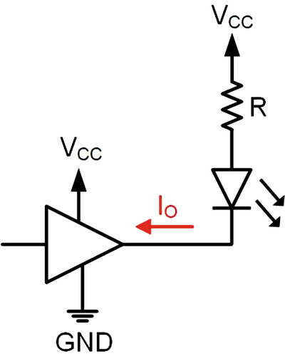
Driver configuration 8

-
3.4.58
For the LED driver configuration shown in Fig. 3.43 where an output of LOW on the driver will turn on the LED, what is the output current (IO) if VCC = +5v, R = 100 Ω, and the LED has a forward voltage of Vf = 1.9v?
-
3.4.59
For the LED driver configuration shown in Fig. 3.43 where an output of LOW on the driver will turn on the LED, what is the output current (IO) if VCC = +5v, R = 1kΩ, and the LED has a forward voltage of Vf = 1.9v?
-
3.4.60
For the LED driver configuration shown in Fig. 3.43 where an output of LOW on the driver will turn on the LED, what is the output current (IO) if VCC = +3.4v, R = 50 Ω, and the LED has a forward voltage of Vf = 1.9v?
-
3.4.61
For the LED driver configuration shown in Fig. 3.43 where an output of LOW on the driver will turn on the LED, what is the output current (IO) if VCC = +3.4v, R = 100 Ω, and the LED has a forward voltage of Vf = 1.9v?
-
3.4.62
For the LED driver configuration shown in Fig. 3.43 where an output of LOW on the driver will turn on the LED, what is the output current (IO) if VCC = +3.4v, R = 1kΩ, and the LED has a forward voltage of Vf = 1.9v?
-
3.4.63
For the LED driver configuration shown in Fig. 3.43 where an output of LOW on the driver will turn on the LED, if VCC = +5v, R = 75 Ω, Vf = 1.9v, and IO-MAX = 25 mA, is the maximum output current specification violated?
-
3.4.64
For the LED driver configuration shown in Fig. 3.43 where an output of LOW on the driver will turn on the LED, if VCC = +5v, R = 150 Ω, Vf = 1.9v, and IO-MAX = 25 mA, is the maximum output current specification violated?
-
3.4.65
For the LED driver configuration shown in Fig. 3.43 where an output of LOW on the driver will turn on the LED, if VCC = +5v, R = 500 Ω, Vf = 1.9v, and IO-MAX = 25 mA, is the maximum output current specification violated?
-
3.4.66
For the LED driver configuration shown in Fig. 3.43 where an output of LOW on the driver will turn on the LED, if VCC = +3.4v, R = 75 Ω, Vf = 1.9v, and IO-MAX = 15 mA, is the maximum output current specification violated?
-
3.4.67
For the LED driver configuration shown in Fig. 3.43 where an output of LOW on the driver will turn on the LED, if VCC = +3.4v, R = 150 Ω, Vf = 1.9v, and IO-MAX = 15 mA, is the maximum output current specification violated?
-
3.4.68
For the LED driver configuration shown in Fig. 3.43 where an output of LOW on the driver will turn on the LED, if VCC = +3.4v, R = 500 Ω, Vf = 1.9v, and IO-MAX = 15 mA, is the maximum output current specification violated?
-
3.4.69
For the LED driver configuration shown in Fig. 3.43 where an output of LOW on the driver will turn on the LED with VCC = +5v and Vf = 1.9v, calculate the value of the resistor (R) in order to set the current through the LED to be 5 mA.
-
3.4.70
For the LED driver configuration shown in Fig. 3.43 where an output of LOW on the driver will turn on the LED with VCC = +5v and Vf = 1.9v, calculate the value of the resistor (R) in order to set the current through the LED to be 12 mA.
-
3.4.71
For the LED driver configuration shown in Fig. 3.43 where an output of LOW on the driver will turn on the LED with VCC = +5v and Vf = 1.9v, calculate the value of the resistor (R) in order to set the current through the LED to be 15 mA.
-
3.4.72
For the LED driver configuration shown in Fig. 3.43 where an output of LOW on the driver will turn on the LED with VCC = +3.4v and Vf = 1.9v, calculate the value of the resistor (R) in order to set the current through the LED to be 5 mA.
-
3.4.73
For the LED driver configuration shown in Fig. 3.43 where an output of LOW on the driver will turn on the LED with VCC = +3.4v and Vf = 1.9v, calculate the value of the resistor (R) in order to set the current through the LED to be 12 mA.
-
3.4.74
For the LED driver configuration shown in Fig. 3.43 where an output of LOW on the driver will turn on the LED with VCC = +3.4v and Vf = 1.9v, calculate the value of the resistor (R) in order to set the current through the LED to be 15 mA
Author information
Authors and Affiliations
Rights and permissions
Copyright information
© 2019 Springer Nature Switzerland AG
About this chapter

Cite this chapter
LaMeres, B.J. (2019). Digital Circuitry and Interfacing. In: Introduction to Logic Circuits & Logic Design with VHDL . Springer, Cham. https://doi.org/10.1007/978-3-030-12489-2_3
Download citation
DOI: https://doi.org/10.1007/978-3-030-12489-2_3
Published:
Publisher Name: Springer, Cham
Print ISBN: 978-3-030-12488-5
Online ISBN: 978-3-030-12489-2
eBook Packages: EngineeringEngineering (R0)