
Abstract
Controller area network (CAN) data link layer is the interface between CAN physical layer and the microcontroller, containing the actual control software. The interface towards the microcontroller consists of mailboxes for receiving and sending in conjunction with the corresponding flags such as transmission-request-flag, receive-flag, etc., and further status-signal signalling errors, etc. Towards the bus, the interface performs synchronization and arbitration as well as error handling and finally the bitwise receive and transmission of data streams.
Any implementation must be compliant with the standard which is mostly concerned with all bus-related signals and their processing. Nevertheless, there is freedom to the implementers especially with respect to the implementation of the microcontroller interface. Besides, for instance, the number and the architecture of the mailboxes, their message filtering technique differs between many suppliers.
This chapter depicts five different solutions in their details, including a solution for a CAN field-programmable gate array (FPGA) implementation.
Access provided by Autonomous University of Puebla. Download chapter PDF
Keywords
- Controller Area Network (CAN)
- Field Programmable Gate Array (FPGA)
- Message Object
- Bus IP
- Acceptance Filter
These keywords were added by machine and not by the authors. This process is experimental and the keywords may be updated as the learning algorithm improves.
3.1 M_CAN—Modular CAN Controller
The modular controller area network (M_CAN) module was developed to expand Bosch’s well-known family of CAN modules (e.g. the C_CAN module, which is found in many microcontrollers) and support standardized (Automotive Open System Architecture, AUTOSAR) software drivers in particular, as well as applications with multiple CAN channels. The M_CAN module’s internal partitioning in CAN core, Tx Handler, and Rx Handler provides flexibility for easy adaptations to future requirements. CAN messages are stored in a separate memory, the Message RAM, not inside the M_CAN. The M_CAN module is compliant with CAN protocol 2.0 A, B, and ISO 11898-1. Figure 3.1 shows its internal structure.

M_CAN block diagram
All functions specified in the CAN protocol, such as CAN protocol controller state machines as well as the shift registers for transmission and reception, are implemented in the CAN core. This protocol unit has been adopted from earlier CAN modules and is part of a direct line of development that begins with the introduction of the CAN protocol. The CAN core’s interface signals are connected to the rest of the M_CAN via a synchronization logic. This makes it possible to supply the CAN core with a dedicated clock for CAN communication, whereas the rest of the module is in the same clock domain as the host central processing unit (CPU). For example, the CAN core might be operated with an 8 MHz crystal clock while the CPU is supplied with a phase-locked loop (PLL) clock of significantly higher frequency which—to limit noise emission—may also be modulated.
The Tx Handler controls the transmission of messages. The host CPU may set transmission requests for several messages; transmit cancellation is also supported. The Tx Handler then transfers the messages—according to the priority of their identifiers—from the Message RAM to the CAN core’s shift register. Up to 32 dedicated transmit buffers are available. They may—partially or completely—be combined to operate as a transmit first-in-first-out (FIFO) or as a transmit queue. Status information regarding the requested transmissions, including a 16-bit transmit time stamp, may be logged into the optional Tx Event FIFO.
Dedicated receive buffers and up to two receive FIFOs may be configured for the reception of messages, under the control of the Rx Handler. The Rx Handler performs acceptance filtering and transfers received messages into the Message RAM. The following filter types are available for the acceptance filtering:
-
Range filter: Matches for identifiers in the range from start identifier to end identifier.
-
Bit masking: Matches for a specific identifier while some identifier bits may be masked.
-
Dual filter: Matches for two specific identifiers.
-
Dedicated Rx: Matches for the identifier of a dedicated receive buffer.
The filters can each be used as acceptance or as rejection filter; they also decide where accepted messages are to be stored. In total, up to 128 filter elements may be configured for 11-bit identifiers and up to 64 for 29-bit identifiers. This may be combined with a global mask for 29-bit identifiers, in support of J1939 applications. The various filter options allow a targeted filtering of received messages ensuring that only messages which are relevant for the particular node are stored in the Message RAM; others are rejected. The reception time, a 16-bit time stamp, is optionally stored with the message.
The M_CAN module combines both qualities of the “Full CAN” concept and of the “Basic CAN” concept. Received messages are stored in dedicated receive buffers as well as in FIFOs; no software acceptance filtering is needed. The transmit messages may be—depending on the application—stored in dedicated transmit buffers or managed in a transmit FIFO or in a dynamic transmit queue.
A 16-bit timer counter is available to check for timeout conditions in the handling of the receive FIFOs and the Tx Event FIFO. Both the timer counter and the time-stamp generation are clocked, via a prescaler, with multiples (1–16) of the CAN bit time.
The configuration and control of the M_CAN module is done by the host CPU, via the Generic Slave interface. Through this interface, the CPU also reads status information from the CAN core, the Rx Handler, and the Tx Handler. The Generic Slave interface may be connected to 8/16/32-bit CPUs.
The Generic Master interface is used to access the 32-bit-wide Message RAM (single or dual channel). The CPU also has direct access to the Message RAM. The transmit buffers, the Tx Event FIFO, the dedicated receive buffers, the receive FIFOs, and the acceptance filter elements are stored in the Message RAM, outside of the module. The partitioning of the Message RAM can be configured flexibly (see Fig. 3.2). A maximum of 1,216 (32-bit-wide) words can be used per M_CAN module; the minimum size of the RAM is determined by the application.

Message RAM configuration
Gateway (GW) configurations consisting of several M_CAN modules sharing one Message RAM (see Fig. 3.3) can easily be set up. Access conflicts between the M_CANs and the CPU are resolved by the attached RAM Arbiter state machine. No modifications to the M_CAN module are required for their use in a GW. It is also possible to connect several M_CAN modules to the same CAN bus, for example, to enlarge the number of message buffers for that channel.

Connecting several M_CAN modules to a shared single-ported message RAM
The interrupt flags of the M_CAN module signal status or error conditions of CAN core, Tx Handler, and Rx Handler. The interrupt flags may be evaluated by polling, or they may be assigned (individually) to one of two interrupt lines that are connected to the host CPU.
In addition to the normal operating mode, the M_CAN module provides several test modes such as the bus monitoring mode to silently observe the CAN communication or the loop back mode, in which the M_CAN treats its transmitted messages as received messages. Self-test of the internal transmit and receive path is possible without disturbing the communication on the CAN bus. A power-down support (sleep mode) completes the feature list.
The M_CAN’s modular structure makes it easy to add new functions, such as new communication features as CAN with Flexible Data Rate (CAN FD; see Sect. 3.3). Another configuration of the M_CAN, with an additional frame synchronization entity that supports Time-Triggered CAN (TTCAN; see Sect. 3.2), is also available.
More information on Bosch’s Internet Protocol controller area network (CAN-IP) modules can be found at the following URL: http://www.semiconductors.bosch.de/en/ipmodules/can/can.asp
3.2 IFI Advanced CAN
Prior to designing a CAN communication system, some decisions must be made. Is the intention to apply a standard CAN controller, which performs the communication tasks together with a standard CPU, or is it intended to make use of a CPU containing an integrated CAN controller or is it planned to integrate the CAN interface into a field-programmable gate array (FPGA) , perhaps in conjunction with a CPU? In any case, however, an important criterion is to plan carefully how the CAN controller shall be operated in order to avoid the CPU to be loaded with unnecessary tasks. Normally operation of all CAN controllers is based on the same basic principle; some more or less mailboxes are installed along with a couple of filters and masks. IFI Advanced CAN, however, takes another route.
The background for the development of the IFI Advanced CAN is not to launch the n + 1st variation of a standard controller as an application-specific integrated circuit (ASIC) but to combine the flexibility of an FPGA with a high-performing and resources-saving integration. For that purpose, this controller provides multiple parameters, which, in the compilation run for the FPGA code, are chosen in such a way that only those resources of the FPGA are allocated which are really necessary for the application.

IFI Advanced CAN block diagram
This concept starts with the interface between CPU and controller (Fig. 3.4). As this Internet Protocol (IP) core is designed for Altera FPGAs, the interface is a so-called Avalon bus. This is a synchronous bus, allowing a dynamic adaptation of the bus width. When the controller is intended to be used in conjunction with the CPU in an FPGA, it is recommended to apply an Altera NIOSII CPU, which accesses the core with a data width of 32 bits. On the application of an external CPU, a parameter selects the desired data bus width of 8, 16, or 32 bits. This simplifies the connectivity for the designers. The following will not go into details on the architecture of the Avalon bus interface, but the structure of the controller will be enlarged, offering quite some specialties.
3.2.1 Transmit Buffer
For offloading the CPU, a sufficiently large buffer memory is required, which intermediately stores the CAN messages ready for transmission until they are finally transmitted by the CAN cell. For that purpose, most of the CAN cell implementations provide mailboxes into which the messages ready for transmission must be written. If on top the transmission of messages is priority controlled by the controller, a lot of software control is needed to know at what time actually a message had been transmitted. IFI Advanced CAN does not make use of this method, but applies a FIFO instead. The transmission of messages in the same sequence as the CPU generates the messages is not only desired by many communication tasks but also even much easier to handle. The number of messages which can be stored in that FIFO can be controlled by a parameter between 30 and 254. Theoretically, there is a case that due to a very busy CAN bus, a message never may be transmitted because of always losing arbitration. A possible solution to that problem would be to clear the FIFO and rewrite it with a different sequence. However, this would imply that the user always had to know which messages are still waiting in the queue. Even for this case, IFI Advanced CAN provides another way out. Any message can be written into the FIFO in the normal way or a priority identification may be assigned to the messages. Those messages are not written into the back of the FIFO but into the front of the FIFO, while passing the queue. This architecture avoids clearing the FIFO and memorizing the history by software. Therefore, three functions are implemented:
-
Removal of a message from the CAN cell, if it is not currently in the transmission process. That is to say, the bus is busy transmitting another message and that message is waiting to be transmitted or that message had been interrupted by an error frame and must be retransmitted. In both cases, that message can be removed without corrupting any frames.
-
The removed message must be written into the FIFO again as a not-yet-transmitted message in order to guarantee that this message is not lost.
-
The most important message is handed over to the CAN cell for transmission.
In order to make sure that this method is working smoothly even for more than one message only, the FIFO buffer is switched into a last-in-first-out structure and identifications are assigned to all messages which are contained in the buffer. The identification enables the controller to recognize which messages still must be transmitted. This concept enables the CPU to insert easily the messages into the buffer while still maintaining control on the transmission. Each message ready for transmission is written into the FIFO as a sequence of four addresses each 32 bits long containing the following information:
-
The addresses 2 and 3 reserve space for 8 data bytes.
-
The address 1 contains the standard or the extended ID.
-
The address 0 contains the data length code and the remote transmit bit as well as an optional frame number. By this number, the controller knows whether transmission of this message must be controlled. In order to activate this function any number greater than 0 must be inserted. After a successful transmission and independently of any filter conditions, the controller writes this message into the receive buffer together with this number and a 32-bit-long time stamp, if desired. Writing into address 0 automatically enables transmission of the message.
Removing a message from a CAN cell can also be done without inserting another message (Remove Pending Message). In case the node is only alone at the bus, because the communication lines were disconnected, the node would continuously retry to transmit the message. After reconnecting the node, the node would retransmit the message again. A removal of the actual message together with a reset of the transmit FIFO pointer enables once again the setup of the messages to be transmitted. The number of message within the FIFO can also be read back.
3.2.2 Masks and Filters
In order to ease the evaluation of received CAN messages, this controller provides 256 pairs of masks and filters. There is an object number assigned to each of the filter pairs, which is written into the receive buffer after a successful check. Because programming is done in two steps, each of the masks and each of the filters provide an additional bit. When applied, both of the bits must be set, in order to avoid the controller to use non-valid combinations for comparison. This makes sure that masks and filters can be reprogrammed even though the system is running. As only those messages are written into the receive buffer which have passed the filter condition, a filter can be applied as such to pass all messages. Setting a 1 in bit position x of the mask defines that the value of the filter bit and the received Identifier (ID) bit in position x must match. A 0 indicates that the comparison is switched off and the comparator always would indicate a match.
3.2.3 Receive Buffer
The receive buffer is FIFO organized. It can be parameterized to be 32–256 messages long. Each message is stored as a sequence of four messages.
-
The address 0 contains the 8-bit-long frame number for messages which had been transmitted by this controller itself, the object number as an identification which of the filters had passed this message, the remote frame bit, as well as the data length code.
-
The address 1 contains the standard and extended ID.
-
The addresses 2 and 3 contain the received data bytes.
-
An additional address allows the receive time stamp of the message to be read.
In contrast to the transmit buffer, the FIFO pointer is only set to the next message after confirmation of the read process by writing into a dedicated address. This technique allows multiple read of each message as well as free choice of the sequence without the risk to lose data. Reading and clearing of the pointer is provided in order to give any kind of control support to the applicant besides information on interrupts.
3.2.4 Time Stamp
The FIFO implementation of transmit and receive buffers safeguards the chronological sequence of the messages. But at any time for any message the generation of a time stamp can be activated or a time stamp be read back respectively, in case the application requests more precise information. Not all systems operate under the same constraints; therefore, the time base is supplied by an external signal, which internally is fed into a 32-bit counter. The actual value of the counter is stored and assigned to the message when the acknowledge bit is recognized. This counter can be separately read and reset for synchronization purposes.
3.2.5 Conclusion
Depending on the application, either the standard component or the FPGA solution may be better suited. Nevertheless, there are more and more arguments arguing for an FPGA implementation. One of the pro-FPGA implementation arguments may be the cancellation of standard components; another one is the continuously decreasing costs of new FPGA product families. Furthermore, FPGAs provide an enormous flexibility with respect to the number of required interfaces. If an application requires more than one CAN node, just implement the number of CAN-IP cores as needed. Furthermore, the increasing complexity of FPGAs offers new possibilities up to the implementation of a complete system on one chip. In order to reduce development time to a reasonable degree while complexity is rising, the application of IP cores becomes a major issue.
The purchase of an IP core should not be based only on trust but on the option to check the functionality before buying. Altera supports this option with its OpenCorePlus concept. The desired IP core can be applied and tested without any restrictions as long as the FPGA is connected to the programming device. After cutting this connection, the controller will still continue to operate for another hour until it automatically stops. Another disadvantage of a standard component is that it only provides exactly the functionality as specified in the data sheet. The flexibility of the FPGA enables the designer to react on customer requests and to implement new functions if required.
3.3 Renesas RS-CAN
As part of its most recent generation of microcontroller devices, Renesas is introducing a new kind of CAN controller function. In contrast to previous implementations, the RS-CAN module supports shared memory among several channels, flexible sizes of memory areas used, and consequent assignment of FIFO structures.
The RS-CAN module contains a proprietary CAN transfer layer from Renesas which fulfils all the requirements of the ISO 11898, SAE J1939, and CAN 2.0B standards.
Besides its capabilities for the full support of “Full-CAN” or “Basic-CAN” applications, there are interesting new ways the RS-CAN module can be used. Several FIFO structures for reception and transmission allow streamed data processing, and by combining this with the AFL (acceptance filter list), a very efficient CAN controller hardware for GW applications is created.
The RS-CAN naturally also supports the conventional method of message processing via message boxes in both the receive and transmit directions. Here, RS-CAN can handle queued messages (with prioritized sending) concurrently.
The shared memory for all associated CAN channels allows easy transfer of messages and signals from one channel to another. The RS-CAN hardware has a built-in mirroring engine, which can perform this job on the message level without any CPU interaction.
If the shared memory is used consistently, it is possible to assign individual sizes of FIFO memories and filtering lists to the different channels, in order to tailor the amount of memory resources available to each channel. In this way, a channel that needs more data and filter resources can take advantage of another channel needing less of these resources (Fig. 3.5).

RS-CAN architecture
3.3.1 Properties of RS-CAN
One RS-CAN module supports up to eight CAN channels. The most popular implementation includes three channels and its characteristics are described in detail below (see Fig. 3.5).
-
CAN protocol according to ISO 11898 (2.0B active), full functionality for extended identifiers and remote frames.
-
Maximum baud rate: 1 Mbit/s. This baud rate can be achieved using a module clock at 22 MHz and a transfer layer clock at 8 MHz, if the bit timing is set to 8 tq per bit. The transfer layer clock can be derived from a separate clock source, by using a PLL bypass, for example.
-
Identical hardware structure for all derivatives and channel configurations, which allows easy porting of software. Compatible with AUTOSAR requirements.
-
192 receive objects, shared flexibly by user configuration between
-
up to 48 commonly shared receive message buffers for mailbox reception
-
up to eight commonly shared receive FIFO units, variable in depth up to 128 messages per FIFO
-
up to three multi-purpose FIFO units per channel (nine in total), variable in depth up to 128 messages per FIFO.
-
-
192 applicable acceptance filtering rules, including 29-bit identifier masking, masking for remote and extended frames, data length control (DLC) filtering, and GW hardware routing rules. Up to eight-way reception is possible, so that a received message can be stored into up to eight different locations in parallel, including an additional software identifier (Hardware Receive Handle (HRH) number of AUTOSAR COM stack processing).
-
16 transmit message buffers per channel (in total 48 buffers), assigned flexibly by user configuration to either
-
one transmission queue per channel (three in total), using a variable subset of the transmit message buffers
-
up to three multi-purpose FIFO units per channel (nine in total), variable in depth up to 128 messages per FIFO
-
up to 16 standard (direct) transmit message buffers per channel (48 in total).
-
-
16 transmit history list (THL) entries per channel.
-
Many interrupt sources, including:
-
global error interrupt for DLC errors and lost messages
-
reception interrupt for each receive FIFO unit (fill level of FIFO is adjustable individually)
-
reception interrupt for each multi-purpose FIFO unit (fill level of FIFO is adjustable individually)
-
transmit interrupt for each multi-purpose FIFO unit (adjustable either on every message, or on the last sent message)
-
transmit interrupt for each transmission queue (adjustable either on every message, or on the last sent message)
-
transmit interrupt for every channel, where the message buffer is not assigned to a multi-purpose FIFO nor to a transmission queue
-
transmit abortion interrupt for every channel
-
THL interrupt for every channel (adjustable either on every new entry or on fill level)
-
error interrupt for every channel (adjustable on various and multiple error sources).
-
-
Time stamp of reception.
-
Transmission delay timers.
-
Individual activation and deactivation of channels.
-
Diagnostic capability: automatic routing of received messages from selectable or all channels to be output on another (diagnostic) channel.
-
Diagnostic mirroring capability: automatic routing of received and sent messages from selectable or all channels to be output on another (diagnostic) channel.
-
Self-test modes with internal and external (including transceiver) loop, to fulfil ISO safety requirements.
-
Listen-only mode for bus analysis purposes.
3.3.2 Initialization of RS-CAN
3.3.2.1 Operation Modes
The RS-CAN module is able to communicate with several CAN channels, where each channel may have its individual configuration. For this reason, besides the global operation mode, there are operation modes for each channel. After a hard reset, the RS-CAN module is globally disabled, which means that all operation modes are set to sleep mode. As a general rule, the operation modes of the channels always follow the global operation mode in the direction of shutdown or stopping, but the channels can only be moved into the activation direction if the global operation mode already has this state.
Sleep Mode
After its entry upon a hard reset, the RS-CAN module automatically initializes its local RAM, where messages, lists, queues, and configurations are stored. Consequently, all settings are well defined to start up values. There is no need to clear any memory with software. The completion of the initialization process is indicated by a flag.
The sleep mode disables the channels’ clocking in order to save power effectively.
Reset Mode
In this mode, the configuration can be changed. Global reconfiguration covers the definition of the memory usage and global behaviour, such as setting the AFL.
Within the channels, the reset mode allows users to set communication parameters such as bit timing.
Operation Mode
A channel can be put into operation mode if this mode has already been set globally. At this point, the CAN channel starts its communication on the CAN bus.
3.3.2.2 Test Modes
Within the operation mode of a channel, several test modes are available besides regular operation.
Listen-Only Mode
All transmit functionality is disabled. This is also effective for the bus acknowledgement and error/overload reporting on the CAN bus by the transfer layer. The CAN channel behaves as a listener on the CAN bus, but it cannot be seen by other bus participants. It is possible to use this mode to detect a valid baud rate among a known selection.
Self-Test Modes
RS-CAN distinguishes between external and internal loops within the self-test modes. In general, the self-test modes are used to verify the functionality and safety of the RS-CAN with software.
The internal loop modes allow internal communication to enable internal transmitted messages to be received either in the same channel (using emulated bus acknowledgement) or by other internal channels. In internal loop mode, the CAN transceiver is not included, and the test messages are invisible for the other CAN bus participants.
In external loop mode, the CAN transceiver is also included in the test loop.
In all self-test modes, the transfer layer is fully included in the test path.
3.3.3 Transmission of Messages
RS-CAN includes four methods of sending messages: the classical use of message buffers, sending from a transmit queue, streamed sending through a FIFO, and automated routing by hardware (diagnostic and mirroring function). There are 16 transmit message buffers available for each channel, and these are used and shared for all these methods of sending messages. By means of sharing, all four sending methods can be enabled at the same time for a channel. Thus, by sharing a channel between several software applications, each application can use its favourite method. The priority of transmission is evaluated on message-buffer level; this means that all four methods of sending are in competition with each other according to the priority rules, but every method may have its internal rules as well.
Figure 3.6 shows an example of a valid usage of the message buffers and how they can be shared among the different sending methods.

Transmission of messages
3.3.3.1 Sending from Message Buffers
Every message buffer that has not been assigned to a transmit (TX) queue, a FIFO or to automated GW routing can be used in this way. When sending from a message buffer, this single message competes in priority with the remaining 15 message buffers. The message buffer stores all the information required to generate a valid and complete frame on the CAN bus.
In addition, there is a flag to enable the generation of an entry in the THL after successful transmission, and there is an optional pointer value (usable as AUTOSAR HTH), which will appear in the THL, too. This allows tracing and defined processing of transmit objects.
3.3.3.2 Sending from Transmit Queues
Several message buffers can be grouped to form a transmit queue, always starting with the uppermost buffer. Within this type of transmit queue, software simply writes all its messages into one single message buffer (the uppermost one), and the RS-CAN hardware performs the sending according to priority rules. This method has the advantage that the software does not need to check for a free message buffer. RS-CAN indicates the fill state of the transmit queue.
3.3.3.3 Sending from Multi-Purpose FIFO
A multi-purpose FIFO in transmit mode (TX) has its own memory area to queue up messages. Again, software writes into a single location to feed in the messages, and the RS-CAN hardware takes care of sending and fill-level indication. The difference between this and the transmit queue is that within a FIFO, the sequence of messages will be kept, ignoring any priority rule (message identifier). One transmit message buffer must be assigned to a FIFO.
3.3.3.4 Sending from GW FIFO
If a multi-purpose FIFO is operated in GW mode, it can be assigned to be a reception target for other CAN channels, so that selected messages from them can be routed to it. In this configuration, the RS-CAN hardware performs all the tasks for this message routing without any necessary software interaction. Again, one transmit message buffer must be assigned to every multi-purpose FIFO.
The key prerequisites for smooth operation of the GW are that incoming messages are well selected from the channels by using the appropriate access filtering list (AFL) settings, and that the bus transport capacity of the output CAN channel is sufficient.
There is only one task that remains for the software, and this is the supervision of the FIFO overflow. If the configuration of the CAN channels allows (at least temporarily) more data to be routed through the hardware GW than the output channel can transmit, the FIFO may run into overflow, so that messages are lost.
3.3.3.5 Transmit History List
Every sent message can be recorded in the THL. The THL represents the confirmation for the software that a message has been sent and acknowledged by another CAN bus participant. The THL can generate interrupts on new entries or on fill level.
3.3.3.6 Transmission Intervals
When using the FIFO methods for sending messages, the minimum interval between two subsequently sent messages can be defined by an internal timer in RS-CAN. This functionality is required to fulfil Transport Protocol requirements of ISO 15765-2 and to avoid a full bus load caused by one node.
3.3.4 Reception of Messages
The reception of messages in RS-CAN is possible using several methods, but every method begins in the filtering section of the multi-reception handler. Here, the AFL determines where a received message will go. For each received message, the AFL is parsed for a match. If a match is found, the associated AFL entry contains up to eight storage targets, which can be loaded in parallel with the message. Valid storage targets are reception FIFO units, multi-purpose FIFO units, and a selectable receive message buffer.
An AFL entry is shown in Fig. 3.7.

Access filtering list entry
The AFL entry stores identifier values (ID) for the standard and extended identifier frame formats of CAN, and associated mask flags, where the relevance of each identifier bit (including remote flag bit RTR and extended flag IDE) can be masked. Masked bits will be set as “don’t care” for the filtering; this works like a so-called wildcard.
Reference DLC values can be entered for DLC checking. If a received message matches the ID, but does not have enough data bytes as specified in the DLC specification of the AFL entry, it will not pass the filter.
Furthermore, the AFL entry contains several pointers:
-
A flat RX direction pointer with its associated enable flag (FE). If FE is set, the message will be stored in the receive message buffer with the number of the pointer value.
-
One or several FIFO direction pointers. Here, each bit represents one of the available receive or multi-purpose FIFO units where the message can be stored.
-
An additional pointer (PTR) value which is a freely configurable value. This value will be attached as a property with the message, so that an identification of the message is possible. This functionality corresponds with the HRH values of AUTOSAR communication stacks.
3.3.4.1 Reception into a Receive Message Buffer
The receive message buffer stores the whole message including the PTR value and a reception time stamp. Old data within the buffer are overwritten.
The method of storing a message in a receive message buffer is designed to be used in conjunction with polled message reception, i.e. for non-interruptive information, which is read and checked by software at certain intervals.
3.3.4.2 Reception into a FIFO Unit
This kind of reception is used for streamed and interruptive data processing. Sorting into different FIFO units makes it possible to distinguish between higher and lower priority messages. Every FIFO unit can be configured when its interrupt is generated, depending on its fill level, even on every reception. Overflow of a FIFO is indicated, too.
Like the message buffers, a FIFO entry also contains the PTR value and the reception time stamp of the received message.
When receiving into a multi-purpose FIFO unit, hardware GW operations are possible. If enabled within a multi-purpose FIFO, its received messages can be transmitted by another channel.
-
In diagnostic mode, a multi-purpose FIFO can collect received messages from one or several channels and send them to another channel.
-
In loop back and mirroring mode, a multi-purpose FIFO collects received and transmitted messages from one (loop back) or several (mirror) channels, and sends them to another channel.
-
At the same time, while performing the hardware GW functions, the messages can be copied into a standard receive message buffer, so that software can monitor all messages processed by the GW.
3.3.5 Summary
The RS-CAN module handles the increased complexity of current requirements for CAN controllers. Streamed data processing support for GWs with high efficiency is combined with flexibility in usage. Greatly enhanced filtering methods and shared resources for all channels allow RS-CAN to be adapted to most application needs. At the same time, the new structure of the RS-CAN hardware is smaller than those of its predecessors.
3.4 Infineon’s CAN Modules of the XC16x- and XC2000/XE16x family
In this section, a short introduction to the two actual CAN modules of Infineon will be given. Both standards comply to “CAN 2.0B active”. At the end of the section, an example how to do a GW application with an XC2000/XE16x family device (a 16/32-bit-microcontroller family with up to CAN nodes) is shown.
3.4.1 TwinCAN and MultiCAN from Infineon
The CAN modules of the current Infineon microcontroller families from Infineon are defined in a scalable approach. The CAN modules have a message control block and separated nodes, building one module. There it is possible to append the message objects to the node, wherever they are needed. It is possible to build FIFO message buffers as well as an automatic rerouting of messages, the so-called GW function. The GW does not cost any CPU performance.
The implementation of the TwinCAN module can be found on the XC16x microcontroller family. The MultiCAN module is available on the XC2000 family as well as on the 32-bit TriCore controllers and last but not least on the 8051-based family, the XC8xx microcontrollers. Therefore, a porting of CAN code among the families is given.
3.4.2 TwinCAN
The TwinCAN module can handle standard as well as extended identifiers. It is able to receive and transmit all identifier types.
-
All 32 message objects:
-
All message objects can be assigned to one of the two CAN nodes.
-
All message objects can be used to receive or transmit.
-
All message objects can be part of a FIFO structure with a size of power of two.
-
All message objects do have a local acceptance mask.
-
All message objects do support frame counters for bus analysis (for example, statistics).
-
All message objects can be part of a GW.
-
All message objects can be used for remote monitoring in the GW use case.
-
-
Up to eight interrupt nodes can be assigned to interrupt events.
-
All nodes support the analyser function (listen mode).
First, the structure of the module is shown. The TwinCAN module is having a block of 32 message objects and two independent CAN nodes. Additional control logic makes these three blocks to act as one module. Figure 3.8 shows the basic block diagram of the TwinCAN module.

Basic block diagram of the TwinCAN module
We start with a brief description of the message object function.
3.4.2.1 Message Objects
Each message object has a local acceptance mask. Therefore, it is possible to receive a group of identifiers. The acceptance mask is ANDed to the identifier. A 0 on a bit position means “don’t care” for the TwinCAN module. Message objects can be part of a FIFO, a GW or one message object can build also a so-called Shared GW. It is also possible to combine the FIFO and the GW feature. Each message object can trigger a receive or a transmit interrupt.
Each message object can be part of a FIFO, which is described here.
3.4.2.2 FIFO
With the TwinCAN module, the FIFO can consist of 2, 4, 8, 16, or 32 message objects. In a system, where specific messages or message groups are coming in, in a high frequency, the FIFO gives the possibility to buffer these messages until the CPU is ready to read out these messages. The probability of overwriting messages can be reduced. During reception, the CPU is not used, until the interrupt is triggered, at a predefined level. The FIFO is also available for transmission, so that the CPU can write all messages to be sent within one block and the TwinCAN module will take care of the transmission to the bus.
In addition to the FIFO, a rerouting function is available, the so-called GW mode (Fig. 3.9).

FIFO block diagram
3.4.2.3 Automatic GW
The GW function of the TwinCAN module allows interconnecting two different bus systems. These two bus systems are allowed to run on different baud rates. No CPU load will be generated. A message received on bus A will be copied to bus B and depending on the settings, the transmission request can be set automatically; the amount of data bytes can be reduced and/or the identifier can be changed automatically. This feature is quite useful also in combination with the GW feature. The FIFO/GW combination allows to reroute messages automatically between two buses running at different speeds, without overwriting message objects, or to buffer their contents via software.
Figure 3.10 shows an example of the speed; information can be automatically forwarded from the Powertrain module to the door module, to lock the door at speeds greater than 30 km/h automatically.

Example: CAN gateway for automotive
In the following example, a message block of four messages having the same identifier shall be routed to a bus running at a lower baud rate.
3.4.2.4 FIFO/GW Combination
To route the messages from bus A to bus B (Fig. 3.11) in an optimal way, a message object assigned to bus A has to be configured a source GW object and to point to a four-state FIFO, assigned to bus B. This combination allows rerouting the messages automatically and it does not cost any CPU performance after initialization. The received messages are copied to the FIFO and the message will be sent according to CAN prioritization rules. Software activities are only needed, in case the data bytes are changed. No software interaction is needed, in case the data length core or the identifier is changed. Be aware that in case the data length code is increased, the new data byte will include a 0 × 0, if not changed by software.

FIFO/gateway running at different speeds
3.4.2.5 Shared-GW-Modus
In case of sporadic messages, which shall be rerouted to the other bus, it is possible to configure a single message object to be a GW. This is the so-called Shared GW Mode. If a message is received, the message object switches to transmission on the second CAN node. The message is sent according to CAN prioritization rules. Depending on the settings, it switches back automatically. This feature only exists on TwinCAN but not on its successor, the MultiCAN module.
Another feature of the TwinCAN module is the so-called analyser mode.
3.4.2.6 Analyser Mode
Starting with TwinCAN, a so-called analyser mode has been introduced to Infineon-microcontrollers. It is comparable to a listen-only mode. This feature gives the possibility to switch a CAN node silent. The CAN node will listen to bus and save the understood messages with the corresponding identifiers into the message objects, but is not taking part actively on the bus. The node will not send any acknowledgement or any error signalling to the bus. If a baud rate detection is implemented, this mode can be used to switch the node silent during the detection phase and not to spam the bus with error messages. If the CAN module becomes active, the analyser feature needs to be disabled, but not the complete node needs to be reconfigured.
With this feature, it is also possible to have both nodes on the very same bus, but only one node is active. With the help of the reception on the second node, a software comparison can be done. This is useful in case of safety application (higher levels) to guarantee the correct reception. The analyser feature can also be applied to disconnect a failing node which permanently disturbs communication from the bus in order to enable the remaining still functional system to continue communication.
3.4.2.7 The Interrupt System
TwinCAN has 72 interrupt sources; 32 interrupt sources are for reception and another 32 for transmission, as the very same message object can trigger a receive as well as a transmit interrupt. (In case of a remote frame) For each CAN node, four status and error interrupts are existing. The interrupt generation of the TwinCAN module allows to have up to eight independent interrupt routines as eight interrupt nodes can be assigned. Therefore, it is quite easy to have a well-defined prioritization among the events. Thus, it is possible to assign a Peripheral Event Controller (PEC) or Direct Memory Access (DMA) to a special message object, without having a complete interrupt routine and having a fast copy process from the TwinCAN to the needed memories.
The successor of the TwinCAN module is the MultiCAN module. The MultiCAN module can be found on the XC2000/XE16x family, the XC8xx family, and on all devices of the Audo Next Generation, Audo Future, and Audo MAX family. By having the same CAN module over all families, the software compatibility of over 8-, 16-, and 32-bit microcontrollers is given to a high extent.
3.4.3 MultiCAN
Like for the TwinCAN module, first the core functions of the module will be explained briefly before discussing the most important point in very detail.
The MultiCAN module offers:
-
CAN functionality, which is V2.0B active.
-
A CAN bus analyser mode and baud rate detection mechanisms for each CAN node.
-
Up to 256 (dependent on the device) message objects that
-
can be assigned to the CAN nodes
-
can be used for transmission or reception
-
offer the remote monitoring mode in case of GW
-
have “Frame Counter Monitoring”.
-
-
Acceptance filtering:
-
Each message has its own local mask, which allows to receive a group of messages.
-
Each message object is able to receive and transmit messages in standard or extended format, and by masking also both types can be received via the very same message object.
-
It is possible to have different prioritization rules on the internal arbiter, running on the message objects.
-
Each message object can be part of a FIFO of any size. The only limitation is the absolute amount of message objects. The message objects are part of a double-chained list and the FIFO is done in the very same structure. The double-chained lists can be changed during runtime.
-
Each message object can be part of a GW, rerouting messages from one CAN bus to another.
-
The list/a part of list can be rerouted to another CAN node at any time.
-
Up to 16 interrupt nodes can be assigned to interrupt sources within the module.
-
The MultiCAN module can include up to 256 message objects and eight CAN nodes. Depending on the implementation, the amount of CAN nodes and message objects can be different from one controller to another. For example, a XC878 included two CAN nodes and 32 message objects, a TC1167/TC1767 has two CAN nodes and 64 message objects, the TC1797 has four CAN nodes and 128 message objects and most family members of the XC2000/XE166 family are available with six CAN nodes and 256 message objects. All members of the Audo MAX family do include the MultiCAN module. Like the TwinCAN module, the module is split between node logic and message objects. Node logic and the message objects are combined and made on module by the control logic. The message objects can be freely assigned to any of the nodes. However, they are not part of a static structure, which is controlling the message objects, but they are part of a list structure. Therefore, it is possible to reassign message objects during runtime, but also to have FIFOs of any size. Figure 3.12 shows a block diagram of the module.

Block diagram of the MultiCAN module
Like on TwinCAN, each message object has a local mask, giving the possibility to receive a group of message identifiers. The flexibility of the FIFO has been increased by using the list structure within the module. Therefore, all message objects (against TwinCAN being limited) can be part of a FIFO, GW, or FIFO/GW combination. The message objects can be scattered over the RAM and do not need to be behind each other.
Figure 3.13 shows an example, with a FIFO consisting of message objects 5, 16, and number 3. Message object 5 is the source object. The source object does not need to be part of the FIFO. Message object 3 is the end of the list and, therefore, pointing to itself. The current position within the FIFO is shown by the pointer CUR(rent). The terminology in Fig. 3.13 is identical to that in the User’s Manual.

List structure of the MultiCAN
With the help of the list structure, a GW can be built. In contrast to TwinCAN, the number of the message object is no longer relevant to build such a GW.
As on TwinCAN, the FIFO and the GW feature may be combined to a GW/FIFO feature. By using the list structure, it is possible to change the FIFO size during the runtime to react flexibly on different busloads. For example, in case that a diagnosis is activated, a different set of message identifiers becomes relevant and the software is able to react to this change.
3.4.3.1 Advantages of the MultiCAN
Besides the already explained list structure, the MultiCAN module is also having an analyser mode. This allows, for example, auto-baud detection or supervision of incoming traffic for safety applications with a second node. A module internal counter also allows calculating the amount of time quanta within one bit. By having such a function, the automatic baud rate detection becomes easier.
On MultiCAN, a feature has been introduced to measure the actual transceiver delay and to check if the bus termination is properly done. By being able to measure the time between a falling edge being transmitted by the CAN node, until this falling edge is received, the actual transceiver delay can be measured.
3.4.3.2 MultiCAN Supports CAN-Debugging
For safety critical applications, MultiCAN is giving some possibilities to support fault tolerant implementations. An example is shown within this section.
If two CAN nodes are connected to the very same bus, we do have the possibility as shown in Fig. 3.14.

System with two redundant CAN nodes connected with two transceivers (left) as well as system with only one transceiver (right)
Two CAN nodes, via two CAN transceivers, are connected to the very same bus (Fig. 3.14, left). The advantage is at the same time the disadvantage of the concept. Two transceivers are used, which means higher cost. As one module shall only listen to bus, the transmit line does not need to be connected. The comparison between the messages is done via software. Due to the fact that two transceivers are used, also transceiver errors can be found, as two transceivers are used.
In the right part of Fig. 3.14, a similar approach is shown, having only one CAN transceiver. The advantage is on the cost side, having only one transceiver. The disadvantage remains that here transceiver errors cannot be found.
In case of having two separate modules, small disturbances can be seen on both nodes at the very same time; therefore, such an issue remains undetected. The MultiCAN module helps to overcome the absolute synchronism.
3.4.3.3 MultiCAN in Analyser Mode
As already described, the CAN node is only listening to the bus, if it is switched to the analyser mode. It is not actively participating in bus traffic. The message objects are assigned to the nodes. If the application needs a higher safety level and, therefore, has to test if messages are properly received, two nodes have to be on the same bus, receiving the same messages, and the application has to compare the received information. As the nodes are transferring the information not exactly at the very same time, short time disturbances can be detected. Therefore, an erratic behaviour between the protocol machine and the nodes can be detected. The amount of unknown errors, relevant for high-level safety applications can be decreased (only necessary in case of Safety Integrity Level 3, SIL3, or Automotive Safety Integrity Level C, ASIL C, and higher). This concept can be implemented with one or two transceivers, depending on the safety level. A possible solution is shown in Fig. 3.15; the grey line shows the solution with two transceivers. Node A is taking part in the bus traffic, whereas node B is in the analyser mode. The messages are saved with a small offset; therefore, short time disturbances become detectable. If further redundancy is needed, both CAN nodes can be connected, so that in case of a failure on node A, node B can take over and signal the situation to the network and, in case required, take over the role of the active node. These concepts are especially interesting for safety applications, for example, with the TC1387 designed for ASIL C and SIL 3 applications.

MultiCAN in analyser mode
In addition, the MultiCAN can be used to detect errors within bus termination. The time between the first dominant edge and the sample point can be measured (Fig. 3.16) with the frame counter, so bus extensions are made easier.

Tx to Rx measurement
The analyser mode and the measurement of bus termination help to detect faulty transceiver circuitries on a bus system.
3.4.3.4 MultiCAN: Flexible Interrupts
MultiCAN has up to 16 interrupt nodes, called Service Request Nodes (SRN), which can be assigned to interrupt events on the MultiCAN module. Each message object can cause an interrupt on receive, transmit, or both. The frame counter can be used to get time and message information. It is also having an overflow interrupt, to enable a better monitoring of the CAN traffic. Therefore, the initialization is assigning interrupt events (Fig. 3.17) to interrupt nodes. All used interrupt sources are mapped to an interrupt node (an interrupt node can handle more than one interrupt source). This is done via bit-field setting. It is also possible to keep some interrupt nodes on polling, but to handle others within an interrupt routine.

Assignment of interrupts
By having this variety of interrupt sources and interrupt nodes, it is possible to have, for example, status information on a lower interrupt level or to poll these, but, for example, error situations like a bus-off (Alert, ALRT) can be handled on higher priority levels. Therefore, an appropriate reaction to an event can be assigned.
3.4.4 The XC2000 Family in GW Applications—An Application Example Using MultiCAN
Microcontrollers of the XC2000/XE16x family do have the “C166SV2 Core” with MAC (multiplier-accumulator, set of digital signal processor (DSP) functions) unit. The very high-end one even includes a cache. They are the logical progression of the previous C16x and XC16x family. The CPU and the peripherals can run up to 128 MHz. The family members do have different MultiCAN modules, with different amount of nodes and message objects. Most of the family members, besides the very low-end one, do have six nodes and 256 message objects. In addition, depending on the device, up to ten Local Interconnect Network (LIN) buses can be handled, in the very high-end one of the XC2000 family, in which a FlexRay module is integrated.
In this example, the CAN module is having six nodes and 256 message objects. The XC2000 family is a scalable microcontroller family, scalable as the usage of a different package will not cause a change in software.
The following example also works with the TriCore family and, in a restricted way, also with the XC8xx family.
3.4.4.1 GW Between Two CAN Bus Systems
In a GW application, different ways of message rerouting are needed. On the one hand, there are messages, which simply need to be transferred to another bus; these messages can be rerouted by the automatic GW feature. The GW mode is configured to copy the complete message and to transfer it directly afterwards. Here no interaction with software is necessary; all actions can be handled within the hardware. Other messages have to be changed in some of the bytes. In this case, the GW mode needs to be configured in such a way that the transfer to the destination message object takes place, but there is no automatic sending, as the software still needs to do the change. Nonetheless, a software transfer is not necessary. The transfer can be, for example, signalled by an interrupt. The corresponding bytes are changed, a new message transmission is requested, and the message object will take part in the internal arbitration process. Other messages need to be sent with a different identifier; if it is always the very same, this change has to be done in the hardware, by using the feature appropriately. In case the identifier needs to be changed depending on the contents of the message, a software interaction is necessary. The basic actions are comparable to the change of data bytes.

Gateway—example
In Fig. 3.18, a GW consisting of two message objects is shown. Message object 5 is defined as the source object and number 9 as the destination object by the usage of CUR. The different GW transfer features can be used as described above; they can be found within the register MOFCRn (here n = 5).
3.4.4.2 Gateway Between CAN- and LIN-Bus
A LIN-compliant node on the XC2000 is implemented on the USIC (Universal Serial Interface Controller) module. The USIC includes a module internal counter, which eases the baud rate measurement during BREAK signal. The module includes a FIFO structure, which allows in combination with the collision detection feature, to have only a single interrupt for the header and one for the frame response. For frames copied from one bus system (here CAN) to another or signal groups, it also eases the usage of writing to the module, as the information can be written at one time. The application does not need to reserve the occupied message objects for longer times or to buffer the messages within RAM in this case, as they can directly be written to the FIFO of the USIC. A CAN message can be copied in only for transactions from the CAN module to the USIC and then be sent via LIN protocol. The received amount of interrupts can be reduced as the FIFO structure allows not to receive the information byte-wise. The speed difference between CAN bus and LIN is normally quite high in an automotive environment, as the LIN bus has a maximum baud rate of shortly below 20 kBaud. Therefore, buffering LIN messages has a high impact on the application.
3.4.4.3 Gateway from CAN to FlexRay
Depending on the XC2000 family device, it is possible either to use a device internal FlexRay module or to use the CIC-310 as extension device, to enable FlexRay communication. The different baud rates need some buffering, especially transferring data from the time-driven high-speed FlexRay bus to the (compared to FlexRay) low-speed event-driven CAN bus. Here the CAN module internal FIFO structures ease handling the traffic coming from the FlexRay module and have to be sent via CAN bus.
3.4.4.4 Outlook
The MultiCAN module includes several useful extensions against the TwinCAN module. The list structure grants a high degree of flexibility to user and more freedom for CAN applications. The double-chained list-structure enables a highly flexible FIFO structure, as the FIFO elements can be collected among the CAN module. Therefore, the reception on faster CAN bus can be buffered in-between for the transmission on a low-speed bus. The USIC on the XC2000 family rounds out this flexibility to the LIN bus. The external bus controller (EBC) allows attaching an external FlexRay device, if this is not included internally. Therefore, the currently existing serial bus systems widely used in automotive environment are available on the device. The FIFOs within CAN and USIC, which is used for LIN, ease the implementations and reduce the overall CPU load for transferring data from one bus system to another. However, these features become useful not only for automotive applications but also for industrial applications. The MultiCAN is used on several members of the industrial microcontroller families, for example, the TC11xx, XE16x, and XC8xx. These devices are optimized for automation and industrial drivers.
3.5 Xilinx CAN-Controller LogiCORE™ IP
The features of Xilinx CAN Controller are that it:
-
Conforms to ISO 11898-1, CAN 2.0A, and CAN 2.0B standards
-
Supports Industrial (I) and Extended Temperature Range (Q)
-
Supports standard frames (11-bit identifier) as well as extended frames (29-bit identifier)
-
Supports bit rates up to 1 Mbps
-
Transmits message FIFO with a user-configurable depth of up to 64 messages
-
Prioritized message transmission through High-Priority Transmit Buffer
-
Automatic re-transmission on errors or lost arbitration
-
Receive message FIFO with a user-configurable depth of up to 64 messages
-
Acceptance filtering by (a user-configurable number of) up to four acceptance filters
-
Sleep mode with automatic wakeup
-
Loop back mode for diagnostic applications
-
Maskable error and status interrupts
-
Has readable error counters (Fig. 3.19).
Fig. 3.19 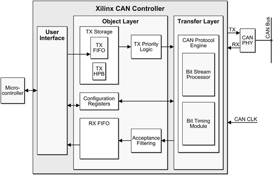
CAN controller block diagram

3.5.1 User Interface
The external interface of the CAN controller is a subset of the Xilinx Intellectual Property Inter-connect (IPIC) signalling. This enables the CAN controller to be interfaced to any microcontroller in a stand-alone mode. When coupled with an on-chip peripheral bus/processor local bus (OPB/PLB) Intellectual Property Interface (IPIF), which attaches to the core through the IPIC interface, the core can be connected to the MicroBlaze. This allows the core to be used in an Embedded Development Kit (EDK) environment. Table 3.1 describes the interface signalling of the CAN controller.
3.5.1.1 Interface Description
The CAN controller supports the following two modes of transfers
-
Single read
-
Single write
3.5.1.2 Single Read Transaction
For a read operation, when the transfer is enabled (Bus2IP_CS = ‘1’ and Bus2IP_RNW = ‘1’), the core samples the address on the Bus2IP_Addr pins and returns the corresponding read data on the IP2Bus_Data pins. Read data are returned on a successive clock rising edge, after a wait time. IP2Bus_Ack is asserted when the data are ready on the IP2Bus_Data pins. For a read operation, it should be noted that address is assumed to be valid on the Bus2IP_Addr pins when Bus2IP_CS is asserted and the core samples the address on the next rising edge of SYS_CLK.
IP2Bus_Ack is asserted for all read transactions, irrespective of whether the transaction is valid or not. Successive read operations require that the Bus2IP_CS be de-asserted and reasserted. The timing diagram for a single read transaction is shown in Fig. 3.20.

Single read transaction
It should be noted that
-
read transactions from address locations defined as reserved return all ‘0’s on the IP2Bus_Data bus,
-
read transactions from write-only address locations return all ‘0’s on the IP2Bus_Data bus,
-
read transactions from the AFR register when C_CAN_NUM_ACF = 0 return all ‘0’s on the IP2Bus_Data bus,
-
read transactions on the Acceptance Filter ID Register (AFIR) and Acceptance Filter Mask Register (AFMR) address locations when C_CAN_NUM_ACF = 0 return all ‘0’s on the IP2Bus_Data bus,
-
read transactions on any or all of the AFIR and AFMR address locations when C_CAN_NUM_ACF > 0 return the data that were written to these locations, and
-
read transactions on an empty RX FIFO return invalid data.
3.5.1.3 Single Write Transaction
For a write operation, when the transfer is enabled (Bus2IP_CS = ‘1’ and Bus2IP_RNW = ‘0’), the core samples both address and data from the Bus2IP_Addr and Bus2IP_Data pins, respectively, and IP2Bus_Ack is asserted on a successive clock rising edge. For a write operation, it should be noted that address on the Bus2IP_Addr bus and data and Bus2IP_Data bus are assumed to be valid when Bus2IP_CS is asserted.
IP2Bus_Ack is asserted for all write transactions, irrespective of whether the transaction is valid or not. Successive write operations require that Bus2IP_CS be de-asserted and reasserted. The timing diagram for a single write transaction is shown in Fig. 3.21.

Single write transaction
3.5.2 Object Layer
3.5.2.1 Transmit and Receive Messages
Separate storage buffers exist for transmit (TX FIFO) and receive (RX FIFO) messages through a FIFO structure. The depth of each buffer is individually configurable up to a maximum of 64 messages.
3.5.2.2 TX High-Priority Buffer
The Transfer High-Priority Buffer (TX HPB) provides storage for one transmit message. Messages written on this buffer have maximum transmit priority. They are queued for transmission immediately after the current transmission is complete, pre-empting any message in the TX FIFO.
3.5.2.3 Acceptance Filters
Acceptance filters sort incoming messages with the user-defined acceptance mask and ID registers to determine whether to store messages in the RX FIFO, or to acknowledge and discard them. The number of acceptance filters can be configured from 0 to 4. Messages passed through acceptance filters are stored in the RX FIFO.
3.5.2.4 Configuration Registers
This module provides access to the registers through the external microcontroller interface.
Table 3.2 defines the CAN controller configuration registers. Each of these registers is 32-bit wide and is represented in big endian format. Any read operations to reserved bits or bits that are not used return ‘0’. A ‘0’ should be written to reserved bits and bit fields not used. Writes to reserved locations are ignored.
3.5.3 Transfer Layer
3.5.3.1 Bit Timing Module
The primary functions of the Bit Timing Logic (BTL) module include:
-
Synchronizing the CAN controller to CAN traffic on the bus
-
Sampling the bus and extracting the data stream from the bus during reception
-
Inserting the transmit bit stream onto the bus during transmission
-
Generating a sampling clock for the Bit Stream Processor (BSP) module state machine
Figure 3.22 illustrates the CAN bit time divided into four parts:

CAN bit timing
-
Sync segment
-
Propagation segment
-
Phase segment 1
-
Phase segment 2
The four bit time parts are comprised of a number of smaller segments of equal length called time quanta (tq). The length of each time quantum is equal to the quantum clock time period (period = tq). The quantum clock is generated internally by dividing the incoming oscillator clock by the baud rate prescaler. The prescaler value is passed to the BTL module through the Baud Rate Presale (BRPR) register. The propagation segment and phase segment 1 are joined together and called ‘time segment1’ (TS1), while phase segment 2 is called ‘time segment2’ (TS2). The number of time quanta in TS1 and TS2 vary with different networks and are specified in the Bit Timing Register (BTR), which is passed to the BTL module.
The Sync segment is always 1-tq long. The BTL state machine runs on the quantum clock. During the start-of-frame (SOF) bit of every CAN frame, the state machine is instructed by the BSP module to perform a hard sync, forcing the recessive (r) to dominant edge (d) to lie in the sync segment. During the rest of the recessive-to-dominant edges in the CAN frame, the BTL is prompted to perform re-synchronization.
During re-synchronization, the BTL waits for a recessive-to-dominant edge. After this is over, it calculates the time difference (number of tqs) between the edge and the nearest sync segment. To compensate for this time difference, and to force the sampling point to occur at the correct instant in the CAN bit time, the BTL modifies the length of phase segment 1 or phase segment 2.
The maximum amount by which the phase segments can be modified is dictated by the Synchronization Jump Width (SJW) parameter, which is also passed to the BTL through the BTR. The length of the bit time of subsequent CAN bits is unaffected by this process. This synchronization process corrects for propagation delays and oscillator mismatches between the transmitting and receiving nodes. After the controller is synchronized to the bus, the state machine waits for a time period of TS1 and then samples the bus, generating a digital ‘0’ or ‘1’. This is passed on to the BSP module for higher level tasks.
3.5.4 Bit Stream Processor
The BSP module performs several MAC/logical link control (LLC) functions during reception (RX) and transmission (TX) of CAN messages. The BSP receives a message for transmission from either the TX FIFO or the TX HPB and performs the following functions before passing the bit stream to BTL:
-
Serializing the message
-
Inserting stuff bits, cyclic redundancy check (CRC) bits, and other protocol-defined fields during transmission
During transmission, the BSP simultaneously monitors RX data and performs bus arbitration tasks. It then transmits the complete frame when arbitration is won, and retrying when arbitration is lost. During reception, the BSP removes stuff bits, CRC bits, and other protocol fields from the received bit stream. The BSP state machine also analyses bus traffic during transmission and reception for Form, CRC, ACK, Stuff, and Bit violations. The state machine then performs error signalling and error confinement tasks. The CAN controller will not voluntarily generate overload frames but will respond to overload flags detected on the bus. This module determines the error state of the CAN controller: Error Active, Error Passive, or Bus-off. When TX or RX errors are observed on the bus, the BSP updates the transmit and receive error counters according to the rules defined in the CAN 2.0 A, CAN 2.0 B, and ISO 11898-1 standards. Based on the values of these counters, the error state of the CAN controller is updated by the BSP.
3.5.5 Configuring the CAN Controller
This section covers the various configuration steps that need to be performed to program the CAN core for operation.
The following are some of the key configuration steps:
-
Choose the mode of operation of the CAN core.
-
Program the configuration registers to bring up the core.
-
Write messages to the TX FIFO/TX HPB.
-
Read messages from the RX FIFO.
3.5.5.1 Programming the Configuration Registers
The following steps are to be performed to configure the core when the core is powered on or after system reset or software reset.
-
1.
Choose the mode of operation
-
Write a ‘1’ to the LBACK bit in the Mode Select Register (MSR) and ‘0’ to the SLEEP bit in the MSR to choose loop back mode.
-
Write a ‘1’ to the SLEEP bit in the MSR and ‘0’ to the LBACK bit in the MSR to choose sleep mode.
-
Write ‘0’s to the LBACK and SLEEP bits in the MSR to choose normal mode.
-
-
2.
Configure the Transfer Layer Configuration Registers
-
Program the Baud Rate Priscilla Register and the BTR to correspond to the network timing parameters and the network characteristics of the system.
-
-
3.
Configure the AFRs
The number of AFMR and AFIR pairs that are used is chosen at build time. To configure these registers, the following steps should be taken:
-
Write a ‘0’ to the UAF bit in the AFR register corresponding to the AFMR and AFIR pair to be configured.
-
Wait till the ACFBSY bit in the Status Register (SR) is ‘0’.
-
Write the appropriate mask information to the AFMR.
-
Write the appropriate ID information to the AFIR.
-
Write a ‘1’ to the UAF bit corresponding to the AFMR and AFIR pair.
-
Repeat the steps mentioned above for each AFMR and AFIR pair.
-
4.
Write to the Interrupt Enable Register (IER) to choose the bits in the Interrupt Status Register (ISR) that can generate an interrupt.
-
5.
Enable the CAN controller by writing a ‘1’ to the CEN bit in the Software Reset Register (SRR).
3.5.5.2 Transmitting a Message
A message to be transmitted can be written to either the TX FIFO or the TX HPB. A message in the TX HPB gets priority over the messages in the TX FIFO. The TXOK bit in the ISR is set after the CAN core successfully transmits a message.
-
1.
Writing a Message to the TX FIFO
-
Poll the TXFLL bit in the SR. The message can be written into the TX FIFO when the TXFLL bit is ‘0’.
-
Write the ID of the message to the TX FIFO ID memory location (C_BASEADDR + 0 × 030).
-
Write the DLC of the message to the TX FIFO DLC memory location (C_BASEADDR + 0 × 034).
-
Write the Data Word 1 of the message to the TX FIFO DW1 memory location (C_BASEADDR + 0 × 038).
-
Write the Data Word 2 of the message to the TX FIFO DW2 memory location (C_BASEADDR + 0 × 03C).
-
Messages can be continuously written to the TX FIFO until the TX FIFO is full. When the TX FIFO is full, the TXFLL bit in the ISR and the TXFLL bit in the SR are set. If polling, the TXFLL bit in the SR should be polled after each write. If using interrupt mode, writes can continue until the TXFLL bit in the ISR generates an interrupt.
-
2.
Writing a Message to the TX HPB
-
Poll the TXBFLL bit in the SR. The message can be written into the TX HPB when the TXBFLL bit is ‘0’.
-
Write the ID of the message to the TX HPB ID memory location (C_BASEADDR + 0 × 040).
-
Write the DLC of the message to the TX HPB DLC memory location (C_BASEADDR + 0 × 044).
-
Write the Data Word 1 of the message to the TX HPB DW1 memory location (C_BASEADDR + 0 × 048).
-
Write the Data Word 2 of the message to the TX HPB DW2 memory location (C_BASEADDR + 0 × 04C).
-
After each write to the TX HPB, the TXBFLL bit in the SR and the TXBFLL bit in the ISR are set.
3.5.5.3 Receiving a Message
Whenever a new message is successfully received and written into the RX FIFO, the RXNEMP bit and the RXOK bits in the ISR are set. In case of a read operation on an empty RX FIFO, the RXNEMP bit in the ISR is set.
-
1.
Reading a Message from the RX FIFO
The RXOK or RXNEMP bits in the ISR can be polled. In interrupt mode, the reads can occur after the RXOK or RXNEMP bits in the ISR generate an interrupt.
-
Read from the RX FIFO memory locations. All the locations must be read regardless of the number of data bytes in the message.
-
Read from the RX FIFO ID location (C_BASE_ADDR + 0 × 050).
-
Read from the RX FIFO DLC location (C_BASE_ADDR + 0 × 054).
-
Read from the RX FIFO DW1 location (C_BASE_ADDR + 0 × 058).
-
Read from the RX FIFO DW2 location (C_BASE_ADDR + 0 × 05C).
After performing the read, if there are one or more messages in the RX FIFO, the RXNEMP bit in the ISR is set. This bit can either be polled or generate an interrupt. The process mentioned above should be repeated till the FIFO is empty.
3.5.5.4 CAN Graphical User Interface
The CAN graphical user interface (GUI) provides a single screen for configuring the CAN core. Parameter C_BASEADDR defaults to X”00000000” in the GUI, while the parameter C_HIGHADDR does not exist (Fig. 3.23).

LogiCORE
3.5.5.5 Component Name
Base name of the output files generated for this core. The name must begin with a letter and be composed of the following characters: a–z, A–Z, 0–9, and “-”.
3.5.5.6 Xilinx CAN Controller Design Parameters
To obtain a CAN controller that is uniquely tailored to the minimum system requirements, certain features can be parameterized. This results in a design that utilizes only the resources required and gives the best possible performance. The features that can be parameterized in the CAN controller are shown in Table 3.3. The interface parameters C_BASEADDR and C_HIGHADDR need to be specified only when the core is interfaced to the OPB IPIF. For the core generated by CoreGen, C_BASEADDR defaults to X”00000000”. C_HIGHADDR parameter does not exist for CoreGen cores.
Number of Acceptance Filters
Valid range is from 0 to 4. This specifies the number of acceptance filter pairs used by the CAN controller. Each acceptance filter pair consists of a mask register and an ID register. These registers can be configured so that a specific Identifier or a range of Identifiers can be received. This determines the value of C_CAN_NUM_ACF.
TX FIFO Depth
Valid values: 2, 4, 8, 16, 32, 64. This configures the depth of the TX FIFO.
The TX FIFO depth is measured in terms of the number of CAN packets. For example, TX FIFO with a depth of 2 can hold at most two CAN packets. This determines the value of C_CAN_TX_DPTH.
RX FIFO Depth
Valid values: 2, 4, 8, 16, 32, 64. This configures the depth of the RX FIFO. The RX FIFO depth is measured in terms of the number of CAN packets. For example, RX FIFO with a depth of 2 can hold at most two CAN packets. This determines the value of C_CAN_RX_DPTH.
3.5.6 Ordering the CAN Controller
A free evaluation version of the CAN core is provided with the Xilinx CORE Generator, which lets you assess the core functionality and demonstrates the various interfaces of the core in simulation. After purchase, the core may be downloaded from the Xilinx IP Center for use with the CORE Generator v9.2i and higher. The CORE Generator is bundled with ISE Foundation v9.2i software at no additional charge. Contact your local Xilinx sales representative for pricing and availability about the CAN LogiCORE module or go to the CAN product page www.xilinx.com/systemio/can/index.html for additional information.
Author information
Authors and Affiliations
Corresponding author
Editor information
Editors and Affiliations
Rights and permissions
Copyright information
© 2013 Springer-Verlag London
About this chapter
Cite this chapter
Lawrenz, W., Hartwich, F., Kelling, U., Krishna, V., Lieder, R., Riekert, P. (2013). Data Link Layer Implementation. In: Lawrenz, W. (eds) CAN System Engineering. Springer, London. https://doi.org/10.1007/978-1-4471-5613-0_3
Download citation
DOI: https://doi.org/10.1007/978-1-4471-5613-0_3
Published:
Publisher Name: Springer, London
Print ISBN: 978-1-4471-5612-3
Online ISBN: 978-1-4471-5613-0
eBook Packages: Computer ScienceComputer Science (R0)