
Abstract
A novel multidirectional low cost coordinated multi-point radio over fiber communication system architecture based on photonic decuple frequency and optical delay interference is proposed and deduced theoretically. At the switching center station, the multi-order photonic millimeter wave is generated by a double arm Mach-Zehnder optoelectronic modulator, and the characteristics of the multi-order photonic millimeter wave are analyzed and verified. At the base station (BS), two photonic millimeter signals are demodulated by an optical delay interferometer. The one photonic millimeter signal is used for generating fifth order upper spectrum band and fifth order lower spectrum band via an optical filter, and then the electronic millimeter signal with 30 GHz is generated by photonic decuple frequency technique. The other photonic millimeter signal is separated into two optical signals via an optical splitter, which are used for generating the third order lower spectrum band signal and the third order upper spectrum band signal respectively. After transmitting 30 km in a SSMF, the clear eye diagram and the good bit error rate are obtained for downlink signal, uplink signal and BS to BS link signal. Thanks to the photonic decuple frequency technique, the cost of the local oscillator with ultra-high frequency is greatly reduced at the BS. Because of no laser optical source, the complexity of the BS is simplified. Owing to the coordinated multi-point technique, ultra-high speed transmitting between the mobile station and the BS can become a reality on the edge of the cell.
1 Foreword
Because the demand for high-speed broadband network and convenient wireless communication increase rapidly, the deep integration of optical fiber communication and wireless communication has gradually become a trend for the future Ultra high speed wireless access networks (Yang et al. 2012; Yeh et al. 2011a, b; Chen et al. 2010). For the wireless access networks, owing to good transmission characteristics, low power consumption, low cost, and lots of available unlicensed bandwidth (Zhu et al. 2011; Li et al. 2015; Xie et al. 2010; Fang et al. 2013), radio over fiber (ROF) transmission system with 24–60 GHz millimeter wave has obtained more and more attention. For the sake of simplifying the complexity of the BS and reducing the cost of the subsystem, it is a good scheme of transmitting optical signal and radio frequency signal synchronously in a same integrated communication network platform. Consequently, the integrated access network systems based on optical fiber communication and wireless communication have investigated recently (Chang et al. 2009; Fang et al. 2012; Zhang et al. 2010). However, they not only consume too many photoelectric transceivers but also use expensive ultra-high frequency local oscillator (LO) at the BS. In addition, the problems of weak signal intensity, serious signal fading, and low communication rate are arise on the edge of the cell.
In the article,we propose a novel coordinated multi-Point radio over fiber (CoMP-ROF) which is based on photonic decuple frequency and optical delay interference. At the SCS, the multi-order photonic millimeter wave is generated by photonic coherence modulation via a double arm Mach-Zehnder optoelectronic modulator. At the BS, two photonic millimeter signals are demodulated by an optical delay interferometer, and then the electronic millimeter signal with 30 GHz used for transmitting downlink wireless signal is generated by photonic decuple frequency technique via a photoelectric detector. And the laser optical sources used for the uplink and the BS to BS link are filtered by two optical filters respectively. We theoretically analyze the principle of the photonic millimeter wave based on photonic decuple frequency technique. We evaluate the bit error rate (BER) performances of the downlink signal, uplink signal and BS to BS link respectively. The communication system network can solve the problems of weak signal intensity, serious signal fading, and low communication rate on the edge of the cell.
2 Fundamental principle and process
Figure 1 show the principle and process of the generation of photonic millimeter wave based on photonic decuple frequency. A continuous photonic wave signal with an angle frequency \(\omega_{0}\) is generated by a DFBL (DFBL, distributed feedback laser), The field of continuous photonic wave signal is described as \(E_{0} \left( t \right) = A_{0} \times e^{{j\omega_{0} t}}\). Here \(A_{0}\) is the continuous photonic wave signal field amplitude. A 3 GHz sinusoidal signal which is generated by a SSG (SSG, Sine Signal Generator) is mixed with an electrical data signal \(A\left( t \right)\) which is generated by a DSG (DSG, Digital Signal Generator), here \(A\left( t \right) = \left[ { - 1 \;or\; 1} \right]\). And then the mixed signal is split up into the up and down path signals, apply the up path signal to the upper arm of a \(LiNbO_{3}\)-DMZM (\(LiNbO_{3}\)-DMZM, LiNbO3-Dual arm Mach Zehnder Modulator). The power of the down path signal is reduced by an EA (EA, Electronic Attenuator) with the gain of -1 dB. And then apply the reduced signal to the lower arm of the \(LiNbO_{3}\)-DMZM simultaneously. The two applied to the upper and lower arm of \(LiNbO_{3}\)-DMZM signals can be described by: \(V_{1} = A\left( t \right) \times A_{L0} \times sin\left( {\omega_{L0} \times t} \right)\), \(V_{2} = A_{Gain} \times A\left( t \right) \times A_{L0} \times sin\left( {\omega_{L0} \times t} \right)\). Here \(A_{Gain}\). is the attenuated amplitude of the power attenuator, and \(A_{L0}\) and \(\omega_{L0}\) are the amplitude voltage and the angular frequency of the 3 GHz sinusoidal signal which is used as a LO (LO, Local Oscillator). The DC (DC, Direct Current) of \(V_{B1}\) or \(V_{B2}\) is adjusted to obtain a constant photonic phase of \(\varphi_{DC} = 2k \times \pi \left( {k = 1,2,3 \ldots } \right)\) to suppress the even ordered or odd ordered photonic sidebands (Qi et al. 2006; Cartledge et al. 1994). According to Refs. Zhu et al. (2011), Li et al. (2015), Xie et al. (2010) and Fang et al. (2013), the photonic filed of the output of \(LiNbO_{3}\)-DMZM can be described as:

Principle and process of 30 GHz photonic millimeter wave based on photonic decuple frequency. DSG digital signal generator, SSG sine signal generator, FM frequency mixer, DFBL distributed feedback laser, EA electronic attenuator, LiNbO 3 -DMZM LiNbO3-dual arm Mach Zehnder modulator
Here \(V_{\pi }\) is the half wave voltage of the \(LiNbO_{3}\)-DMZM. \(\gamma\) is the optical power splitting ratio of the two arms of the \(LiNbO_{3}\)-DMZM. \({{\alpha }}\) is the insertion loss of the \(LiNbO_{3}\)-DMZM. For an ideal \(LiNbO_{3}\)-DMZM, its optical power splitting ratio is equal to 0.5, and the optical insertion loss is approximately equal to 0.
Because the output of the photonic spectrum via the \(LiNbO_{3}\)-DMZM depend on the driving bias voltages and \(\theta\), here the \(\theta\) is the electronic relative phase, so we can adjust them to generate photonic millimeter wave with different spectra. Form Eq. (1), and the output of the photonic filed can be described as:
Here \(m = \frac{{\pi \times V_{LO} }}{{V_{\pi } }}\) is the photonic phase modulation index, \(\varphi_{1} = \frac{{\pi \times V_{B1} }}{{V_{\pi } }}\) and \(\varphi_{2} = \frac{{\pi \times V_{B2} }}{{V_{\pi } }}\) are each constant phase shifts that are caused by DC bias voltages \(V_{B1}\) and \(V_{B2}\) respectively. And so the modulated photonic wave can be expressed as:
On the condition of \(A\left( t \right) = \left[ { - 1 or 1} \right]\), when n is odd, \(J_{n} \left( m \right)\) is becomes odd function, and when n is even, \(J_{n} \left( m \right)\) is even function. Set the electrical relative the switching bias voltage, the switching RF (RF, Radio Frequency) voltage and the bias voltages of \(LiNbO_{3}\)-DMZM to be \(V_{SB} = 4{\text{V}}\),\(V_{SRF} = 0.5{\text{V}}\), \(V_{B1} = 0{\text{V}}\), \(V_{B2} = 4{\text{V}}\). And so the output of the photonic field can be written as:
On the basis of Eq. (4), we can get the following three conclusions. First, only odd ordered photonic spectral sidebands carry useful data information, however, even ordered photonic spectral sidebands do not carry the useful data information. Second, the output of the \(LiNbO_{3}\)-DMZM have no zero ordered center photonic spectral sideband, second ordered photonic spectral sideband and fourth ordered photonic spectral sideband. Third, odd ordered photonic spectral sidebands carry data information via optical phase shift modulation, and the modulated photonic signal is insensitive to optical intensity modulation, so the odd ordered photonic spectral sidebands can be used for uplink laser light source which is modulated by electrical high speed RF signal for uplink transmission via photoelectric intensity modulator. At the BS (BS, Base Station), the optical information signal transmitted from the SCS (SCS, Switching Center Station) is divided into two paths by a 1:1 optical splitter. Through the one path, we utilize upper fifth and lower fifth ordered photonic spectral sidebands to generate 30 GHz Photonic millimeter wave via high performance photoelectric detector. Through the other path, we use the lower third and upper third ordered photonic spectral sideband signals for the laser optical sources of uplink and BS to BS link respectively.
3 The CoMP-ROF network system and simulation analysis
The experimental setup based on computer simulation for the integrated full duplex CoMP-ROF communication network system which is based on optical delay interference and photonic decuple frequency is shown in Fig. 2. And the spectrum diagram of the key nodes (A), (B), (C), (D), (E), (F), (G), (H) and (I) in the functional block diagram of the CoMP-ROF communication network system are shown in Fig. 3.

Functional block diagram of the CoMP-ROF communication network system. SCS switching center station, BS base station, DSG digital signal generator, SSG sine signal generator, FM-1 frequency mixer, DFBL distributed feedback laser, EA electronic attenuator, LiNbO 3 -DMZM LiNbO3-dual arm Mach Zehnder modulator, SSMF standard single mode fiber, ODI optical delay interferometer, BPBOF band pass bessel optical filter, IROF inverted rectangle optical filter, EDFA erbium doped fiber amplifier, PD photonic detector, ES electronic splitter, LPBEF low pass bessel electronic filter, BPEF band pass electronic filter, RFPA radio frequency power amplifier, OS optical splitter, ROF rectangle optical filter, MZM Mach Zehnder modulator, RF radio frequency, LO local oscillator

Spectrum diagram of the key nodes in the CoMP-ROF communication network system
In the SCS (SCS, Switching Center Station), a continuous photonic wave with the line width of 10 MHz and the center frequency of 193.1 THz is generated from a 3 dBm DFBL (DFBL, Distributed Feedback Laser). The photonic millimeter wave is generated from the \(LiNbO_{3}\)-DMZM with the extinction ratio of 30 dB and the insertion loss of 5 dB which is modulated by two channels asymmetrical wireless signal via upper arm and lower arm of the \(LiNbO_{3}\)-DMZM. The upper channel wireless signal is generated by a FM-1 (FM, frequency mixer), that is to say, which is produced via sine wave signal generated by a SSG (SSG, Sine Signal Generator) with the angular frequency of 3 GHz (\(\omega_{LO} = 2 \times \pi \times 3\;{\text{GHz}}\)) mixing with a digital baseband signal of 1Gbit/s pseudorandom data sequence with length of \(2^{31} - 1\), here the digital baseband signal is generated by a DSG (DSG, Digital Signal Generator). And except for the power, the lower channel wireless signal is the same as the upper channel wireless signal. The power of the lower channel wireless signal is reduced 1 dB by an EA (EA, Electronic Attenuator). The switching bias voltage of the \(LiNbO_{3}\)-DMZM is 4 V, the switching RF voltage of the \(LiNbO_{3}\)-DMZM is 0.5 V, the modulation voltage1 and voltage2 of the \(LiNbO_{3}\)-DMZM do not enable, the bias voltage1 and bias voltage2 of the \(LiNbO_{3}\)-DMZM are 0 and 4 V(\(V_{B1} = 0\,V\), \(V_{B2} = 4\,V\)). After the \(LiNbO_{3}\)-DMZM, the wireless signal is carried on the odd ordered spectral sidebands while the even order spectral sidebands is restrained. Besides, the even order spectral sidebands no carry the wireless signal. And the power of the third order spectral sidebands is slightly than that of others. The frequency interval between the two fifth order spectral sidebands is 30 GHz. Then the modulated photonic signal is transmitted by the SSMF (SSMF, Standard Single Mode Fiber). Consequently, the results of the computer simulation are consistent with the values of the theoretical derivation. The photonic millimeter wave signal is transmitted 30 km in the SSMF-1 with the dispersion of 16.75 ps/nm/km and the attenuation of 0.2 dB/km.
In the BS-1 (BS, Base Station), the photonic millimeter wave signal is demodulated by an ODI (ODI, Optical Delay Interferometer) with the reference wavelength of 193.1 THz, the insertion loss of 40 dB and the delay time of \(10^{ - 10}\) second, then two channels photonic millimeter wave signal is demodulated from the ODI. The upper channel photonic millimeter wave signal is filtered via a BPBOF (BPBOF, Band Pass Bessel Optical Filter) and an IROF (IROF, Inverted Rectangle Optical Filter). And the central frequency of the BPBOF is 193.1T Hz, the bandwidth of the BPBOF is 40 GHz, the depth of the BPBOF is 100 dB, the central frequency of the IROF is 193.1 THz, the bandwidth of the IROF is 20 GHz, the depth of the IROF is 60 dB. Then the filtered photonic millimeter wave signal is amplified by an EDFA-1 (EDFA, Erbium Doped Fiber Amplifier) with the gain of 15 dB and the noise figure of 5 dB. And then, the amplified photonic millimeter wave signal transform into 30 GHz electronic millimeter wave signal via the PD-1 (PD, Photonic Detector). The 30 GHz electronic millimeter wave signal is split into two signals via an ES (ES, Electronic Splitter). The one signal is filtered by a LPBEF-1 (LPBEF, Low Pass Bessel Electronic Filter) with the cutoff frequency of 0.75 GHz and the depth of 100 dB. Then the filtered signal is utilized for demodulating the digital baseband signal and measuring the BER (BER, Bit Error Rate) of the transmission link via downlink receiver. The other signal is filtered by a BPEF-1 (BPEF, Band Pass Electronic Filter) with central frequency of 30 GHz and width of 2 GHz, and the filtered radio signal is amplified via a RFPA-1 (RFPA, Radio Frequency Power Amplifier), then the amplified RF (RF, Radio Frequency) signal is transmitted by an antenna (Antenna-1).
In the BS-1 (BS, Base Station), the lower channel photonic millimeter wave signal is split into two photonic signals via a 1:1 OS (OS, Optical Splitter), the one photonic signal is filtered by a ROF-2 (ROF, Rectangle Optical Filter) with the central frequency of 193.09 THz. The bandwidth of the ROF-2 is 10 GHz,the depth of the ROF-2 is 100 dB. Then the filtered photonic signal is modulated by a 30 GHz RF signal which is mixed by a baseband data signal of 32Gbit/s pseudorandom data sequence with length of \(2^{31} - 1\) via a MZM-2 (MZM, Mach-Zehnder Modulator). And then, the modulated photonic signal is transmitted to the adjacent BS-2 via the SSMF-3 with the dispersion of 16.75 ps/nm/km and the attenuation of 0.2 dB/km and the length of 30 km.
At the adjacent BS-2, the transmitted photonic signal from the BS-1 is amplified by an EDFA-3 with the gain of 15 dB and the noise figure of 5 dB. The amplified photonic signal transform into electronic signal via the PD-3. The detected electronic signal is filtered by a LPBEF-3 with the cutoff frequency of 0.75 GHz and the depth of 100 dB. And then, the filtered electronic signal is utilized for demodulating the base band data signal of 32Gbit/s pseudorandom data sequence with length of \(2^{31} - 1\) and measuring the BER of the transmission link via BS to BS receiver.
At the BS-1, the other photonic signal which is from the 1:1 OS is filtered by a ROF-1 with the central frequency of 193.11 THz. The bandwidth of the ROF-1 is 10 GHz,the depth of the ROF-1 is 100 dB. And then, the filtered photonic signal is modulated by another 30 GHz RF radio frequency signal which is mixed by another baseband data signal of 32 Gb/s pseudorandom data sequence with length of \(2^{31} - 1\) via the other intensity MZM-1, the modulated photonic signal is transmitted to the SCS via the SSMF-2 with the dispersion of 16.75 ps/nm/km and the attenuation of 0.2 dB/km and the length of 30 km.
At the SCS, the transmitted photonic signal from the BS-1 is amplified by an EDFA-2 with the gain of 15 dB and the noise figure of 5 dB. The amplified photonic signal transform into electronic signal via the PD-2. The detected electronic signal is filtered by a LPBEF-2 with the cutoff frequency of 0.75 GHz and the depth of 100 dB. And then, the filtered electronic signal is utilized for demodulating the base band data signal of 32Gbit/s pseudorandom data sequence with length of \(2^{31} - 1\) and measuring the BER of the transmission link via uplink receiver.
At the MS (MS, Mobile Station), there are diversity antenna-2, antenna-3, RFPA-2, RFPA-3, ES-2, BPEF-2, FM-2 and LO (LO, Local Oscillator). The wireless communication links between the BS-1 and the MS and between the BS-2 and the MS are established via the diversity antenna-2 and antenna-3 of the MS and the antenna-1 of the BS-1 and the antenna-4 of the BS-2. Especially, when the BS-1 is on the edge of the coverage area which is generated by the BS-1, the CoMP-ROF system will start the CoMP (CoMP, Coordinated Multi-Point) function. The CoMP-ROF function of the system is not only establishing the communication links to send and receive radio signal between the MS and the BS-1 and between the MS and the BS-2, but also letting the BS-1 transmit a part of the information to the adjacent BS-2 via the SSMF-3 at the same time. The part of the information from the BS-2 and the rest of the information from the BS-1 are transmitted to the MS via free space propagation synchronously. Obviously, the function not only can reduce the rate of dropping, but also make the transmission rate doubled at the edge of the coverage area which is generated by the base station. The optical spectrum measured at the key nodes (A), (B), (C), (D), (E), (F), (G), (H) and (I) are shown in Fig. 4a–i respectively.


Spectrums at different positions: a after \({\text{LiNbO}}_{3}\)-DMZM, b after the upper channel of ODI, c after the lower channel of ODI, d after BPBOF, e after IROF, f after ROF-2, g after ROF-1, h after MZM-2 and i after MZM-1
The BER of the downlink signal, uplink signal and BS to BS link signal are gauged via downlink receiver, uplink receiver and BS to BS receiver respectively. Figure 5a shows the curve graph of the relationship between the BER of downlink signal and the transmitting photonic power. Figure 5b shows the curve graph of the relationship between the BER of uplink signal and the transmitting photonic power. Figure 5c shows the curve graph of the relationship between the BER of BS to BS link signal and the transmitting photonic power.

The curve graphs of the relationship between the transmitting power of the DFBL and the BER of a downlink signal, b uplink signal, and c BS to BS link signal
4 Illustration and discussion
The CoMP-ROF communication system architecture based on photonic decuple frequency and optical delay interference has been proved by rigorous theory and computer simulation. The simulation software is OptiSystem produced by Optiwave Ltd. Canada, and it is a professional development suite for optical communication system. At present, Optisystem is widely used by scientific research institutions and the global well-known system integrated communications companies. In this paper, these data are calculated by the simulation software, the graphs are processed via EXCEL2010, and the system diagrams are drawn via WORD2010. The laser and photoelectric modulator are the most important two active devices in the whole system, and then, we begin to study and discuss the relationships between the key parameters of the two devices and the BER of the transmission system.
-
1.
The relations between the center frequency of the DFBL and the BER of the transmission links.
The center frequency of the DFBL in the simulation system is 193.1 THz, however, the center frequency of the DFBL will be very small fluctuations in the actual working. To this end, we have done computer simulation about the fluctuation of center frequency influencing the BER of the transmission links. The precondition is that the other parameters of the system must be the same as the third part of the paper.
Figure 6a shows the curve graph of the relationship between the BER of downlink signal and the center frequency of the DFBL. Figure 6b shows the curve graph of the relationship between the BER of uplink signal and the center frequency of the DFBL. Figure 6c shows the curve graph of the relationship between the BER of BS to BS link signal and the center frequency of the DFBL.
Fig. 6 
The curve graphs of the relationship between the center frequency of the DFBL and the BER of a downlink signal, b uplink signal, and c BS to BS link signal
From Fig. 6, we can see that the BER of the downlink is greatly influenced by center frequency fluctuation of DFBL. However, the BER of the uplink and BS to BS link are almost unaffected, and the performances of the BER are very good. In the Fig. 6a, when the center frequency deviates from 193.1 THz, the BER of the downlink is deteriorating rapidly. Under the condition of ensuring the effective data transmission, we also can get from the graph that the tolerance of center frequency deviation is about ±1GH.
-
2.
The relations between the line-width of the DFBL and the BER of the transmission links.
When the other parameters of the system are the same as the third part of the paper, Fig. 7 show the curve graphs of the relationship between the line-width of the DFBL and the BER of downlink signal, uplink signal, and BS to BS link signal.
Fig. 7 
The curve graphs of the relationship between the line-width of the DFBL and the BER of a downlink signal, b uplink signal, and c BS to BS link signal
From Fig. 7a, we can see that the narrower the line-width is set, the lower the BER becomes. That is to say, the better performances of the transmission link are obtained. However, due to the restrictions of the production process and technology, the line-width of the DFBL is impossible to achieve a very narrow level. And in the actual test, the 10 MHz nominal narrow line-width of the DFBL is also minor change. Under the condition of ensuring the effective data transmission, we also can get from the graph that the tolerance of line-width change is greater than 15 MHz (25–10 MHz = 15 MHz). It can be seen from Fig. 7b, c that the BER of the uplink and BS to BS link are affected little by the line-width fluctuation.
-
3.
The relations between the extinction ration of LiNbO3-DMZM and the BER of the transmission links.
When the other parameters of the system are the same as the third part of the paper, Fig. 8 show the curve graphs of the relationship between the extinction ratio of LiNbO3-DMZM and the BER of downlink signal, uplink signal, and BS to BS link signal. From Fig. 8, we can see that the extinction ratio of LiNbO3-DMZM Photoelectric modulator has almost no influence on the transmission performance of three links.
Fig. 8 
The curve graphs of the relationship between the extinction ratio of LiNbO3-DMZM and the BER of a downlink signal, b uplink signal, and c BS to BS link signal
-
4.
The relations between the switching bias voltage of LiNbO3-DMZM and the BER of the transmission links.
When the other parameters of the system are the same as the third part of the paper, Fig. 9 show the curve graphs of the relationship between the switching bias voltage of LiNbO3-DMZM and the BER of downlink signal, uplink signal, and BS to BS link signal. It is obvious that the switching bias voltage has little effect on the BER of uplink and BS to BS link, and the BER of the two links is maintained at 10−30–10−20. Therefore, the transmission performance of the two links is good. However, the BER of the downlink signal is affected by the switching bias voltage very significantly.
Fig. 9 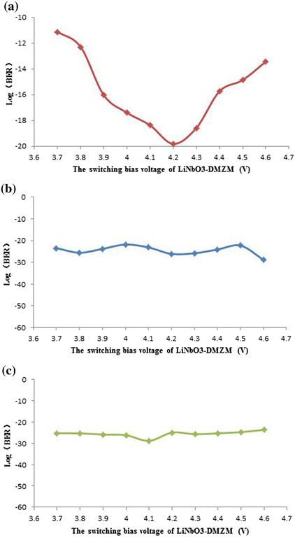
The curve graphs of the relationship between the switching bias voltage of LiNbO3-DMZM and the BER of a downlink signal, b uplink signal, and c BS to BS link signal
From Fig. 9a, we can see that when the switching bias voltage is 4.2 V, the BER of the uplink signal is the best, and when it deviates from the 4.2 V, the BER of the uplink signal will rapidly deteriorate. And it can be seen from the simulation test that the BER of the downlink signal is acceptable when the switching bias voltage is between 3.4 and 5 V. Therefore, the anti-deterioration degree of the switching bias voltage is up to ±20 %.
-
5.
The relations between the switching RF voltage of LiNbO3-DMZM and the BER of the transmission links.
When the other parameters of the system are the same as the third part of the paper, Fig. 10 show the curve graphs of the relationship between the switching RF voltage of LiNbO3-DMZM and the BER of downlink signal, uplink signal, and BS to BS link signal.
Fig. 10 
The curve graphs of the relationship between the switching RF voltage of LiNbO3-DMZM and the BER of a downlink signal, b uplink signal, and c BS to BS link signal
From Fig. 10a, we can see that the BER of the downlink will decrease when the switching RF voltage drop, and the BER of downlink will become large when the switching RF voltage increase; However, as we can see from Fig. 10b, c, the BER of BS to BS link will become smaller when the switching RF voltage increase. And when the switching RF voltage is about 0.5 V, the BER of the three transmission links is probably maintained at the level of 10−20, and it seems to be a good compromised choice for the three links. From Fig. 10a–c, we can also see that the BER of the three transmission links is also acceptable when the deviation degree of the optimal switch RF voltage is about +/-10%.
-
6.
The relations between the bias voltage-1 of LiNbO3-DMZM and the BER of the transmission links.
When the other parameters of the system are the same as the third part of the paper, Fig. 11 show the curve graphs of the relationship between the bias voltage-1 of LiNbO3-DMZM and the BER of downlink signal, uplink signal, and BS to BS link signal.
Fig. 11 
The curve graphs of the relationship between the bias voltage-1 of LiNbO3-DMZM and the BER of a downlink signal, b uplink signal, and c BS to BS link signal
It is obvious that the bias voltage-1 has little effect on the BER of the uplink and BS to BS link, and the BER of the two transmission links is basically maintained between 10−30 and 10−20, and the transmission performance of the signal is good. However, the bias voltage-1 has a great influence on the BER of the downlink. From Fig. 11a, we can see that when the bias voltage-1 is 0 V, the transmission performance of the downlink is best. And the BER is rapidly deteriorating when the parameter deviates from 0 V. However, the BER of the downlink is acceptable when the bias voltage-1 deviates ±0.2 V from the optimal bias voltage-1.
-
7.
The relations between the bias voltage-2 of LiNbO3-DMZM and the BER of the transmission links.
When the other parameters of the system are the same as the third part of the paper, Fig. 12 show the curve graphs of the relationship between the bias voltage-2 of LiNbO3-DMZM and the BER of downlink signal, uplink signal, and BS to BS link signal. From Fig. 12a, we can see that when the bias voltage-2 is 4 V, the BER of the downlink is best, and the BER of the downlink appears to be deteriorating rapidly when the bias voltage-2 deviates from 4 V. From Fig. 12b, we can see that the BER of the uplink will reduce when the bias voltage-2 is reduced, and the BER of the uplink will increase when the bias voltage-2 is increased. From Fig. 12c, we can see that the BER of the BS to BS link will reduce when the bias voltage-2 is increased, and the BER of the BS to BS link will increase when the bias voltage-2 is reduced.
Fig. 12 
The curve graphs of the relationship between the bias voltage-2 of LiNbO3-DMZM and the BER of a downlink signal, b uplink signal, and c BS to BS link signal
From Fig. 12a–c, we can see that the BER of the three transmission links is maintained at the level of 10−20 when the bias voltage-2 is about 4 V. It seems to be a good choice of parameter for the three transmission links. And we also can see that the BER of the three transmission links is still acceptable when the bias voltage-2 deviates ±10% from the optimal bias voltage-2.


5 Conclusion
An unusual multidirectional low cost coordinated multi-point radio over fiber communication system architecture based on photonic decuple frequency and optical delay interference is proposed and deduced theoretically. After transmitting 30 km in the SSMF, the clear eye diagram and the good bit error rate are obtained for downlink signal, uplink signal and BS to BS link signal. The transmission rates of the uplink and BS to BS link are as high as 32 Gb/s. Thanks to the photonic decuple frequency technique, the cost of the local oscillator with ultra-high frequency is greatly reduced at the BS. Because of no laser optical source, the complexity of the BS is simplified. Owing to the coordinated multi-point technique, ultra-high speed transmission between the mobile station and the BS can become a reality on the edge of the cell.
References
Cartledge, J.C., Rolland, C., Lemerle, S., Solheim, A.: Theoretical performance of 10 Gb/s lightwave systems using a III-V semiconductor Mach-Zehnder modulator. IEEE Photonics Technol. Lett. 6, 282–284 (1994)
Chang, G.K., Chowdhury, A., Jia, Z.S., Chien, H.C., Huang, M.F., Yu, J.J., Ellinas, G.: Key technologies of WDM-PON for future converged optical broadband access networks. J. Opt. Commun. Netw. 1, C35–C50 (2009)
Chen, W.P., Wang, W.F., Hwang, W.S.: Adaptive dynamic bandwidth allocation algorithm with sorting report messages for Ethernet passive optical network. IET Commun. 4, 2230–2238 (2010)
Fang, W.J., Huang, X.G., Yang, K., Zhang, X.M.: Full duplex dense-wavelength-division-multiplexing radio-over-fiber system transmission of 75-GHz W-band frequency multiple-input multiple-output orthogonal-frequency-division-multiplexing signals with 3*12 Gbps downstream and 6 Gbps upstream. Opt. Eng. 51, 095004 (2012)
Fang, W.J., Huang, X.G., Li, G.: A full duplex radio-over-fiber transmission of OFDM signals at 60 GHz employing frequency quintupling optical up-conversion. Opt. Commun. 294, 118–122 (2013)
Li, G., Zhang, X.M., Chen, Y., Huang, X.G.: A bidirectional WDM-PON-ROF communication network architecture based on optical sextuple frequency. Microw. Opt. Technol. Lett. 57, 2079–2083 (2015)
Qi, G., Yao, J., Seregelyi, J., Paquet, S., Belisle, C., Zhang, X., Wu, K., Kashyap, R.: Phase-noise analysis of optically generated millimeter-wave signals with external optical modulation techniques. IEEE J. Lightwave Technol. 24, 4861–4875 (2006)
Xie, J.L., Huang, X.G., Tao, J.: A full-duplex radio-over-fiber system based on a novel double-sideband modulation and frequency quadrupling. Opt. Commun. 283, 874–878 (2010)
Yang, X.S., Huang, X.G., Xie, J.L., Zhu, J.H., Li, G.: Investigation on transmission characteristics of 40 GB/s optical networks based on duobinary modulation. Microw. Opt Technol. Lett. 54, 1355–1359 (2012)
Yeh, C.H., Chow, C.W., Liu, Y.L.: Self-protected ring-star-architecture TDM passive optical network with triple-play management. Opt. Commun. 284, 3248–3250 (2011a)
Yeh, C.H., Chow, C.W., Wu, F.Y., Chi, S.: Using Fabry–Perot laser diode and reflective semiconductor optical amplifier for long reach WDM-PON system. Opt. Commun. 284, 5148–5152 (2011b)
Zhang, L.J., et al.: Broadband convergence of 40 GHz-ROF and 10 Gb/s WDM-PON systems in the duplex access network. Chin. Phys. Lett. 27, 054203 (2010)
Zhu, J.H., Huang, X.G., Xie, J.L.: A full-duplex radio-over-fiver system based on dual quadrupling-frequency. Opt. Commun. 284, 729–734 (2011)
Author information
Authors and Affiliations
Corresponding author
Rights and permissions
About this article

Cite this article
Li, G., Liu, H. A novel CoMP-ROF communication network system based on photonic decuple frequency and optical delay interference. Opt Quant Electron 48, 406 (2016). https://doi.org/10.1007/s11082-016-0673-0
Received:
Accepted:
Published:
DOI: https://doi.org/10.1007/s11082-016-0673-0