
Abstract
This paper presents the design, fabrication and reliability testing of a double spiral platinum-based MEMS hotplate for gas sensing applications. The structure of MEMS hotplate consists of a 0.7 µm-thick thermally grown SiO2 membrane of size 120 µm × 120 µm over which a double spiral platinum resistor is laid out. The hotplate membrane is supported by its four arms connected to the Si-substrate. The design and simulation of the hotplate structure was carried out using MEMS-CAD Tool COVENTORWARE. Based on the design, a double spiral platinum resistor of 103 Ω is fabricated on SiO2 membrane using lift-off technique. The platinum deposition is carried out using DC sputtering technique. Bulk micromachining of Si is done from front side of the structure to create the suspended SiO2 membrane. The temperature coefficient of resistance (TCR) of platinum is measured and found to be 2.19 × 10⁻³/ °C. The TCR value is used for temperature estimation of the hotplate. The test results show that the microhotplate consumes only 20 mW power when heated up to 500 °C. For reliability testing of fabricated structure, the hotplate is continuously operated at 300 °C for 1.8 h. Also, it can sustain at least 61 cycles pulse-mode operation at 530 °C with ultra-low resistance and temperature drifts. The structure can sustain a maximum temperature and current of 611 °C and 11.55 mA respectively without any damage.
1 Introduction
Low power consumption is a basic requirement for a gas sensor. In metal-oxide gas sensors, an elevated temperature is required to activate the gas sensing film. The metal-oxide gas sensors require low power consumption, fast response time and uniform temperature distribution over the sensing material (Puigcorbe et al. 2003). These sensors also require good mechanical stability at high temperatures. Micro electro mechanical systems (MEMS)-based hotplates are most suitable for this purpose and have been widely used in gas sensors because of their low power consumption (Afridi et al. 2002; Belmonte et al. 2006). They are based on micromachined silicon substrate technology which provides: (1) low thermal mass of the substrate, eventually leading to reduced power consumption, (2) thermal isolation and (3) post sensing signal conditioning and actuating circuitry, both integrated on the same chip (Hierlemann 2005; Graf et al. 2007). The MEMS hotplate generally consists of a heater fabricated on a dielectric suspended membrane (Afridi et al. 2002). The incorporation of a suitably designed microheater on to the micromachined platform is a critical step in sensor development technology (Benn 2001; Puigcorbe et al. 2003; Fung et al. 1996; Zhang et al. 2007, 2008). The key technique for fabrication of different types of membranes for microhotplate platform is micromachining (bulk or surface) of silicon (Lang 1996; Payne et al. 1995; McGeough 2001; Paul Davim and Jackson 2010). Surface micromachining provides good mechanical strength and poor thermal isolation whereas bulk micromachining provides good thermal isolation with less mechanical strength. Both wet and dry etching techniques are usually employed for micromachining of silicon. In general, the fabricated dielectric membranes are of two types: (1) micro-bridge or suspended type and (2) closed type. The closed membranes are fabricated by back-side etching of silicon using either deep reactive ion etching (DRIE) technique or wet etching technique. However, the micro-bridges are fabricated by front side etching of silicon. In this type, the active layers are suspended on a cavity through the support of two or four beams. Due to extremely low thermal mass, micro-bridge type membrane consumes lower power than closed membrane (Xu et al. 2011). Also, the suspended membrane is more compatible with CMOS process as there is no requirement of alignment from both sides during lithography process (Simon et al. 2001; Mitzner et al. 2003).
The silicon etching using wet etching technique has low cost in comparison to DRIE technique because in wet etching method, usually some aqueous chemicals are used to etch out silicon selectively. The commonly used silicon wet etchants are potassium hydroxide (KOH), hydrazine-water (N2H4)n solutions, ethylene diamine pyrocatechol (EDP) and tetramethyl ammonium hydroxide (TMAH) (Lang 1996; Payne et al. 1995, McGeough 2001). The selective etching of silicon with less effect on metal can be done using (N2H4)n solutions but it has relatively high toxicity. Potassium hydroxide is an alkali metal hydroxide etchant, which has high etching rate. But, unfortunately it is not compatible with CMOS processing because it attacks the exposed aluminum and contaminates the gate oxide with mobile alkali metal ions. The EDP is a diamine-based etchant, which has the anisotropic etching characteristic by adding a small amount of pyrazine. However, it is a hazardous solution and has long-term toxic effects. TMAH belongs to quaternary ammonium hydroxide group, which fulfills the requirement of CMOS compatibility. It has the advantages of high etch rate, better etch characteristics, less attack on metal, and low toxicity. Now-a-days, most of researchers have reported the bulk micromachining of Si using TMAH (Simon et al. 2001; Mitzner et al. 2003; Tasur et al. 2001; Shikida et al. 2000; Chen et al. 2001; Liebert 2002; Papet et al. 2006; Cheng et al. 2006; Pal et al. 2009). In the present approach, TMAH is selected for bulk micromachining of silicon.
Many researchers have studied the reduction of power consumptions of MHPs by changing the geometry of dielectric membrane (Zhang et al. 2006; Lee et al. 2002; Belmonte et al. 2006; Solzbacher et al. 2000). Among these works, the microheaters are fabricated on a suspended dielectric membrane supported by two or four suspended beams to reduce the power consumption to around 50 mW at 400 °C. But, it is still too high in some applications such as portable gas sensor and wireless sensor networks. Generally, double spiral microheater is preferred for better temperature uniformity (Mele et al. 2012; Creemer et al. 2008). For commercialization of microhotplate, modification of the heater geometry and reduction in power consumption should not be done without addressing the reliability. In other words, for more accurate measurements, the long-term stability of the device is important.
For better stability and reliability of the microhotplate, the resistance drift should be minimum at high temperatures, typically 400 °C, which is mostly used to activate the gas sensing films. This shows that the heater material must be stable at high temperature, typically 400 °C. Platinum is most suitable for this purpose because it offers the advantages of reliability, reproducibility and stable temperature coefficient of resistance (TCR). The platinum-based microheater can handle large current densities and operate up to 550–600 °C without any structural damage (Tiggelaar 2004). It is not attacked by the wet etchants during bulk micromachining of silicon, thereby simplifying the fabrication process. Among most of the above works, the authors have used the suspended type membranes supported by four arms for low power consumption of microhotplates. However, the reliability, long-term stability, pulse-mode operation and current carrying capability of the microheater structures are not reported, which are essential for commercialization of the device. In the present approach, a double spiral platinum-based microhotplate using thin dielectric suspended membrane supported by four arms with low power consumption has been reported. For better temperature uniformity, a double spiral shaped heater was selected. The reliability of the structure such as stability, pulse-mode operation and current carrying capability were tested.
The paper is organized as follows. The design and simulation of the device is presented in Sect. 2. Fabrication and reliability testing of the device are given in Sects. 3 and 4 respectively. Finally, we conclude in Sect. 5.
2 Design and simulation
2.1 Structural design of MHP
The total heat flow in a microhotplate can be expressed as (Simon et al. 2001):
where, Q Conduction is the heat conducted through a closed membrane or a suspended type membrane, Q ambient is the heat conducted through the air, Q radiation is the heat loss due to radiation, and Δx is the unknown heat loss including free convection. Decreasing the heated area (active area) can reduce the power consumption of the microhotplate. In the present simulation, a MEMS-CAD Tool COVENTORWARE was used. For simplicity, only membrane area with platinum resistor was taken into consideration. Analyzer’s MemMech solver of COVENTORWARE was used in the simulation. The solver includes a range of analyses such as thermomechanical analysis, electrothermal analysis, and electrothermomechanical analysis. A microhotplate of dielectric membrane size, 120 µm × 120 µm was designed using COVENTORWARE. A double spiral platinum resistor was laid out on the membrane (Fig. 1). The dimensions used in the design are as follows: heater finger width, 5 µm; gap between fingers, 10 µm; membrane thickness, 0.7 µm and platinum thickness, 0.2 µm. The layout of the hotplate consists of three photomasks: MHP-1 for platinum resistor, MHP-2 for pad opening and MHP-3 for cavity etching.

Microhotplate structure designed using COVENTORWARE
2.2 Simulation of microhotplate
In the simulation of MHP, MemMech solver of COVENTORWARE was used. In the analysis, the temperature surrounding the hotplate was fixed at 300 K as the boundary condition. The material properties used in simulation work were imported from COVENTORWARE library and are given in Table 1. The typical plots of temperature distribution, maximum displacement (in z-axis) and von mises stress at 1.9 V are shown in Fig. 2a–c respectively. The red color shows the maximum values of the parameters. The maximum temperature, maximum displacement (in z-axis) and von mises stress of the hotplate membrane at 1.9 V were found to be 816.6 °C, 2.23 µm and 1,381 MPa respectively. From simulation results, it was also observed that a good uniformity of the temperature is achieved in the active area of the hotplate membrane. The mechanical stress distribution picture shows that the bending portion of the heater has moderately high stress accumulation. The maximum stress is generated at the bending point of the heater. A combined plot of maximum temperature and displacement of the membrane (in z-axis) at different applied voltages ranging from 0.1 to 1.9 V is shown in Fig. 2d. The transient response of the microhotplate was simulated and time taken to reach 380 K from 300 K was found to be less than 1 ms (Fig. 2e). However, the generated stress due to different temperatures is shown in Fig. 2f. It is observed that the generated stress in the hotplate membrane linearly increases with membrane temperature.

Simulation of double spiral microhotplate structure: a temperature distribution at 1.9 V, b displacement at 1.9 V, c von mises stress distribution, d plot of maximum temperature and displacement at different applied voltages ranging from 0.1 to 2.5 V, e transient response and f von mises stress variation with temperature
3 Fabrication of microhotplate
A suspended microhotplate was fabricated on a P-type 〈100〉 Si wafer. The resistivity of P-type wafer was taken as 10–20 Ω cm. The thickness of the silicon substrate was taken as 500 µm. The process flow of the device fabrication, shown in Fig. 3, can be described as follows:

Process flow of the microhotplate: a cleaned Si substrate; b thermally grown SiO2 layer; c Pt resistor and bonding pads patterned by lift-off; d front etching window formed by BHF; e membrane released in TMAH solution
-
1.
The silicon substrate was cleaned using RCA1 and RCA2 cleaning steps by making the solution of deionized water (DI), NH4OH, H2O2 in ratio of 5:3:3 and DI water, HCl, H2O2 in the same ratio, respectively.
-
2.
Thermal oxidation was done to grow a thin SiO2 layer of 0.7 µm thickness for microhotplate membrane. In this process, the substrate was dried with nitrogen gas and loaded in oxidation furnace at temperature 500 °C to avoid any cracks due to rapid temperature change. A sequence of dry-wet-dry cycle of 10 min–90 min–10 min was run in oxidation furnace at 1,050 °C. The O2 gas flow during dry and wet oxidation was 6 SLM (standard liter/min) and 1 SLM respectively. However, during the wet oxidation, O2 gas was bubbled through DI water which was kept at 95 °C.
-
3.
Photolithography (Mask #1) using positive photoresist S1818 was done using MA6 Double Sided Mask Aligner for Pt lift-off. Then, the wafer was subjected to platinum deposition using DC sputtering technique.
-
4.
An adhesive Ti layer of 200 Å thickness was deposited using DC magnetron sputtering. Then a thin platinum layer of 0.2 µm thickness was deposited. The sputtering process parameters during deposition are as follows: base pressure 3.00 × 10⁻⁷ mtorr; power 200 W, deposition pressure 5 mtorr; substrate rotation speed 20 rpm; and deposition temperature 50 °C. After lift-off, the width of resistor fingers and separation between them were found to be 5 and 10 µm respectively. The bonding pad size was taken as 200 µm × 200 µm. Figure 5a shows the fabricated platinum resistor using lift-off technique.
-
5.
Photolithography using Mask #2 was done for cavity etching. The windows for cavity etching were opened in thermally grown SiO2 layer using BHF (Fig. 4a).
Fig. 4 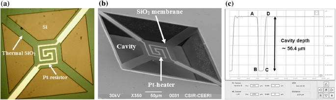
Fabricated structures of double spiral microhotplate: a platinum resistor after lift-off and window opening, b SEM image of suspended membrane with microheater and c cavity depth measured using Dektak 6M surface profiler
-
6.
In the last process step, the membrane was released using an alkaline 25 % (wt) tetra methyl ammonium hydroxide (TMAH) solution with 5 rpm agitation of the wafer holder. The temperature was kept at 85 °C. The total etching time to release the membrane was measured as approximately 2.15 h. A SEM image of fabricated platinum heater on a suspended membrane is shown in Fig. 4b. The cavity depth was measured using Dektak 6 M surface profiler and found to be 56.4 µm, as shown in Fig. 4c. In cavity depth measurement, the stylus of surface profiler goes down from point A to B on side wall of cavity. From point B to C, it moves on the cavity bottom surface and then it starts climbing up from point C to D. The average step height (ASH) from point A to B or C to D was measured as cavity depth.

4 Characterization
4.1 Packaging and TCR measurement
The fabricated wafer with double spiral microheater was diced using DAD 6450 dicing machine. Since the structures were more fragile due to membrane release, therefore before dicing, the cavities in the fabricated wafer were filled with positive photoresist S1818 using spin coating technique. In this way, the microhotplate structures were protected from coolant water flow during dicing. The microhotplate chip was wire bonded and packaged (Fig. 5a). The die was mounted on a TO type 10-pin header using EPO-TEK H20E silver epoxy and cured at 120 °C for 40 min. Thereafter, 1 mil thick gold wires were bonded thermosonically at 120 °C for external connections. In this process, a WestBond Bonder was used.
After wire bonding and packaging, TCR of the platinum heater was measured by electrically heating the device in a temperature-controlled oven. Thereafter, the temperature of the platinum heater was extracted by the following formula:
where, R 1 and R 2 are the heater resistances at temperatures T 1 and T 2 respectively (Afridi et al. 2002).

TCR measurement: a packaged device and b resistance variation with temperature
In this way, both the estimated temperature and average temperature profile of heater element were measured. Though it can not give the exact temperature of the active area of the membrane, this method is still a convenient way to estimate the temperature. The variation of resistance of platinum heater with increasing temperature is shown in Fig. 5b. It is observed that the resistance linearly increases with temperature. Using this variation, the TCR value of platinum was measured as 0.00219 °C−1.
4.2 Power consumption versus temperature
For temperature estimation, the microhotplate chip was placed on a probe station MPS 150, as shown in Fig. 6a. The connecting pads were probed with two electrical probes and different voltages were applied across the microheater. The corresponding current and resistance of the heater were measured. Figure 6b shows the temperature variation with power consumption. It is observed that the microhotplate temperature can go up to 500 °C at 20 mW power consumption. The maximum temperature of 636.7 °C was achieved at 32.17 mW power consumption without any damage to the structure. During electrical testing, the images of active area of microhotplate were captured by high resolution camera at different applied voltages (Fig. 7). The encircled area shows the temperature uniformity of the double spiral microhotplate.

Power consumption of microhotplate: a testing arrangement and b temperature versus power graph

Images of active area of the microhotplate at a 1.8 V and b 2.4 V
4.3 Pusle-mode operation
In general, the normal gas sensing applications require microhotplate operation of about 5 s at 400 °C and 10 s at 100 °C (Bosc et al. 1998). Therefore, the resistance and corresponding temperature drift of microhotplate must be evaluated because of frequent mechanical deformation and thermal cycles. Figure 8 shows the pulse-mode operation of double spiral microhotplate structure. Here, a pulse of 10 s (ton = 5 s and toff = 5 s) is applied to the microhotplate for several cycles. It is observed that the microhotplate can reach the same thermal and mechanical steady state of normal operation after each cycle. A resistance change of about 8.0 Ω and temperature drift of about 9 °C is reflected from resistance and temperature responses respectively (Fig. 8a, b).

Pulse-mode operation of microhotplate: a resistance versus time and b temperature versus time
4.4 Current carrying capability
The current capability of a double spiral microheater fabricated on a suspended membrane supported by four arms must be evaluated for reliability. Figure 9a shows the I–V characteristic of the microhotplate structure. Initially, current increases with increasing applied voltage but, after a certain limit, the current drops drastically because of high resistance of microheater (open circuit). The corresponding temperature of microhotplate increases due to current rise through the element. After a certain limit, the structure of microhotplate was damaged due to high temperature. As a consequence, the current flowing through the heater was drastically reduced to minimum value. Figure 9b shows the damaged structure of microhotplate after passing maximum current through the microheater. The heater burnt out and showed very high resistance to the current path. It is observed that the maximum current of 11.5 mA can pass through the structure without any damage.

Current capability testing of microhotplate: a I–V characteristic and b damaged structure after passing maximum current
4.5 Thermal stability study
Stability of microhotplate was tested by applying constant voltage to the microheater. The change in resistance value of the microheater was recorded by KEITHLEY, Semiconductor Characterization System, 4200-SCS (Fig. 10a). The resistance slightly varies with test time at applied voltage 1.7 V for 1.86 h. A maximum variation of about 4 Ω was measured in 1.86 h test time. The corresponding temperature dependence with test time was calculated using Eq. (2) and is shown in Fig. 10b. It is observed that the double spiral microhotplate suspended structure supported by its four arms showed stable operation at 311 °C for 1.86 h. Due to change in lab temperature, there is a small fluctuation of resistance and temperature dependence in the graphs.

Test results of microhotplate stability: a resistance dependence on test time and b temperature dependence on test time
5 Conclusions
A small size, double spiral, suspended type platinum-based microhotplate supported by four arms has been developed with low power consumption. After dicing and packaging, the TCR value of platinum was measured to estimate the microhotplate temperature. The reliability testing of this type of microhotplate was performed. The performance of the double spiral microhotplate was characterized with respect to power consumption, pulse-mode operation, current carrying capability and stability. In summary, the microhotplate consumed only 20 mW when heated up to 500 °C. It can sustain a maximum current of 11.5 mA without any damage to the structure. This type of microhotplate can sustain at least 61 cycles pulse-mode operation with low resistance and low temperature drifts and has continuously worked for at least 1.86 h.
References
Afridi MY, Suehle JS, Zaghloul ME, Berning DW, Hefner AR, Cavicchi RE, Semancik S, Montgomery CB, Taylor CJ (2002) A monolithic CMOS microhotplate-based gas sensor system. IEEE Sensors J 2(6):644–655
Belmonte CJ, Puigcorb J, Arbiol J, Vila A, Morante JR, Sabate N, Gracia I, Cane C (2006) High-temperature low-power performing micromachined suspended micro-hotplate for gas sensing applications. Sens Actuators, B 114:826–835
Benn G (2001) Design of a silicon carbide micro-hotplate geometry for high temperature chemical sensing, M S thesis, MIT, Cambridge, MA, USA, 2001
Bosc JM, Guo Y, Sarihan V, Lee T (1998) Accelerated life testing for micro-machined chemical sensors. IEEE Trans Rel 47(2):135–141
Chen PH, Peng HY, Hsies CM, Chyu MK (2001) The characteristic behavior of TMAH water solution for anisotropic etching on both Silicon substrate and SiO2 layer. Sens Actuators, A 93:132–137
Cheng D, Gosalvez MA, Hori T, Sato K, Shikida M (2006) Improvement in smoothness of anisotropically etched silicon surfaces: effects of surfactant and TMAH concentrations. Sens Actuators, A 125:415–421
Creemer JF, Briand D, Zandbergen HW, Vlist WV, Boer CR, de Rooi NF, Sarro PM (2008) Microhotplates with TiN heaters. Sens Actuators A Phys 148(2):416–421
Fung SKH, Tang Z, Chan PCH, Sin JKO, Cheung W (1996) Thermal analysis and design of a micro-hotplate for integrated gassensor applications. Sens Actuators A Phys 54(1–3):482–487
Graf M, Barrettino D, Baltes HP, Hierlemann A (2007) CMOS hotplate chemical microsensor. Springer
Hierlemann A (2005) Integrated chemical microsensor systems in CMOS technology. Springer
Lang W (1996) Silicon microstructuring technology. Mater Sci Eng 17(1):1–55
Lee DS, Shim CH, Lim JW, Huh JS, Lee DD, Kim YT (2002) A microsensor array with porous tin oxide thin films and microhotplate dangled by wires in air. Sens Actuators B Chem 83(1–3):250–255
Liebert S (2002) Encapsulation of naked dies for bulk silicon etching with TMAH. Microelectron Reliab 42:1939–1944
McGeough JA (2001) Micromachining of Engineering Materials. Taylor & Francis, NewYork
Mele L, Santagata F, Iervolino E, Mihailovic M, Rossi T, Tran AT, Schellevis H, Creemer JF, Sarro PM (2012) A molybdenum MEMS microhotplate for high-temperature operation. Sens Actuators A Phys 188:173–180
Mitzner KD, Sternhagen J, Galipeau DW (2003) Development of a micromachined hazardous gas sensor array. Sens Actuators B Chem 93(1–3):92–99
Pal P, Sato K, Shikida M, Gosalvez MA (2009) Study of corner compensating structures and fabrication of various shapes of MEMS structures in pure and surfactant added TMAH. Sens Actuators, A 154:192–203
Papet P, Nichiporuk O, Kaminski A, Rozier Y, Kraiem J, Lelievre JF, Chaumartin A, Fave A, Lemiti M (2006) Pyramidal texturing of silicon solar cell with TMAH chemical anisotropic etching. Sol Energy Mater Sol Cells 90:2319–2328
Paul Davim J, Jackson MJ (2010) Nano and micromachining. Wiley, Hoboken
Payne RS, Sherman S, Lewis S, Howe RT (1995) Surface micromachining: from vision to reality to vision. In: Proceedings of IEEE international solid-state circuits conference technical digest, vol 14–17, San Francisco, CA, USA, pp 164–165
Puigcorbe J, Vogel D, Miche B, Vila A, Gracia I, Cane C, Morante JR (2003) Thermal and mechanical analysis of micromachined gas sensors. J Micromech Microeng 13:548–556
Shikida M, Sato K, Tokoro K, Uchikawa D (2000) Differences in anisotropic etching properties of KOH and TMAH solutions. Sens Actuators 80:179–188
Simon I, Bârsan N, Bauer M, Weimar U (2001) Micromachined metal oxide gas sensors: opportunities to improve sensor performance. Sens Actuators B Chem 73(1):1–26
Solzbacher F, Imawan C, Steffes H, Obermeier E, Möller H (2000) A modular system of SiC-based microhotplates for the application in metal oxide gas sensors. Sens. Actuators B Chem 64(1–3):95–101
Tasur JJ, Du CH, Lee C (2001) Investigation of TMAH for front-side bulk micromachining process from manufacturing aspect. Sens Actuators, A 92:375–383
Tiggelaar RM (2004) Silicon-based microreactors for high-temperature heterogeneous partial oxidation reactions, PhD. Dissertation, Univ Twente, Enschede, The Netherlands
Xu L, Li T, Gao X, Wang Y (2011) Development of a reliable micro-hotplate with low power consumption. IEEE Sensors J 11(4):913–919
Zhang FT, Tang Z, Yu J, Jin RC (2006) A micro-Pirani vacuum gauge based on micro-hotplate technology. Sens Actuators A Phys 126(2):300–305
Zhang KL, Chou SK, Ang SS (2007) Fabrication, modeling and testing of a thin film Au/Ti microheater. Int J Thermal Sci 46(6):580–588
Zhang K, Rossi C, Petrantoni M, Mauran N (2008) A nano initiator realized by integrating Al/CuO-based nanoenergetic materials with a Au/Pt/Cr microheater. J Microelectromech Syst 17(4):832–836
Acknowledgments
The authors wish to thank the Director, CSIR-CEERI, Pilani for encouragement and guidance. They are also thankful to all members of MEMS and microsensors group for helpful discussions, technical assistance and support. One of the authors (V. K. Khanna) acknowledges the financial support from CSIR emeritus scientist scheme ES 1314Y1514.
Author information
Authors and Affiliations
Corresponding author
Rights and permissions
About this article

Cite this article
Prasad, M., Khanna, V.K. A low-power, micromachined, double spiral hotplate for MEMS gas sensors. Microsyst Technol 21, 2123–2131 (2015). https://doi.org/10.1007/s00542-014-2393-3
Received:
Accepted:
Published:
Issue Date:
DOI: https://doi.org/10.1007/s00542-014-2393-3