
Abstract
Light-emitting diodes (LEDs) have become the integral part of almost all electrical and electronic systems and gadgets. LEDs of gallium arsenide (GaAs) emitting infrared light were patented by Gary Pitman and Bob Biard of Texas instruments way back in 1961. Since then, efforts have been made continuously in the direction of developing efficient LEDs in the visible and ultraviolet range also. The literature survey shows that during 1970–1979 there was a significant development in red, green, yellow, orange, and blue LEDs. Out of these, blue LED was very expensive and could not be commercialized until 1994. Although inorganic LEDs in the visible region are in use for the past 3–4 decades as replacement of incandescent bulbs, elements in seven segment displays, large RGB displays, calculator, watches, etc., but the main problems are that (i) the processing of basic inorganic semiconductor material is not environment-friendly due to requirement of high purity (ii) non-flexibility (iii) high cost of processing. Therefore, the researchers all over the world focused their research on developing systems and devices in such a way that not only environment is protected (green systems and green devices), but also requirements like flexibility, low-power consumption, and cost effectiveness be taken care of. Conducting polymer-based organic LEDs (OLEDs) and other devices is the alternative for futuristic devices. In fact the work started extensively after Alan G Mac Diarmid, Alan J. Heeger, and Hideki Shirkawa received noble prize in the year 2000 for their research on conducting polymer (polyacetylene). The present article deals with introduction and working of both inorganic and organic LEDs. The emphasis has been given on organic LEDs. Present state of art has been given in detail since its inception. Starting from a single layer OLED to present day multilayer layer OLEDs with different color-to-color tuning have been discussed in detail. The fabrication, relevant characterization techniques and analysis have also been discussed in detail. A systematic development in terms of improvement inefficiency, luminance, stability, and low-power consumption is given which has been possible due to (i) incorporation on some nanomaterials-like carbon nanotubes, quantum dots, graphene (ii) improving and optimizing the physical conditions of growth which include annealing temperature and its duration (iii) incorporation of electron transport layer (ETL), hole transport layer (HTL), electron blocking layer (EBL), hole blocking layer (HBL) in right sequence in the device structure (iv) improving the morphology of the spin-coated films by controlling spin speed and spin duration (v) concentration of conducting polymer in the organic solvent (vi) controlling thickness of the emissive layer, etc. Some light has also been thrown on future aspects and applications of OLEDs.
Access provided by CONRICYT-eBooks. Download chapter PDF
10.1 Organic Light-Emitting Diodes–A Review
With rising population and rising standard of living, the rate of demand of energy increased many fold all over the world in the past two decades, particularly from the year 2000 onwards, and as expected it will continue to do so. Researchers working in the area of energy are making untiring efforts to find environmentally friendly, cheaper, and sustainable ways to produce the energy by non-conventional energy sources in which wind and solar play an important role. The driving force behind it is that the conventional energy sources like coal, oil, and fossil fuel are depleting very fast. Also the techniques to produce electricity are neither ecofriendly, nor these sources have an unlimited stock and unlimited life, and therefore, scientists are generally looking mainly for two approaches:
-
(i)
Finding/utilizing alternative—environmentally friendly techniques using non-conventional sources of energy
-
(ii)
Making/ using daily use appliances and devices which consume very low power as the energy saved is equivalent to energy produced
Solar energy, wind energy, thermal energy, bio-energy are some of the examples of ecofriendly non-conventional sources of energy, whereas use of highly efficient, low-power consuming semiconducting and other useful electronic materials-based devices like light-emitting diodes (LEDs), semiconductor laser, IMPATT and GUNN diodes are examples of energy saving efficient devices. It may be pointed out that in some cases, for example, for lighting purpose researchers are looking for some new materials other than inorganic semiconductors due to the reasons discussed in the following text.
The present chapter deals mainly with organic light-emitting diodes (with special emphasis on white LEDs which may be used for lighting purpose). Here we would like to give a brief introduction and working principle of both inorganic and organic LEDs. An attempt has been made to throw light on the present state of art of organic light-emitting diodes (OLEDs) and plastic light-emitting diodes (PLEDs). The question arises: Why Organic LEDs? The answer is simple and has been explained in the next paragraph.
Although the inorganic semiconductor-based LEDs are commercially available and have become very popular for economic lighting purpose, traffic lights, etc., as cheaper, efficient and less-power consuming alternative to conventional tube lights, bulbs, fluorescent lamps, CFL. In spite of these advantages, there are some serious environmental problems in processing inorganic semiconductor materials which need a very high level of purity (6–8 N) for device application. In case of silicon, which is highly abundant, technologically advanced and highly reliable material for devices, there is lot of carbon emission in its processing for obtaining desired level of purification. So is the case with other semiconducting materials also where toxicity level is undesirable. The higher will be the demand, the more will be damage to the environment—which has already reached the alarming level. Therefore, it is the duty of the present generation to think and take necessary measures in the interest of coming generation and must not leave an unhealthy and polluted environment for them. Therefore, wherever possible the alternative ecofriendly materials and processing techniques should be used for future applications. Organic or plastic electronics seems to have a bright future where organic semiconductors and conducting polymers are the base materials. There are also some stability and efficiency issues, which need to be addressed. In the area of lighting, the organic LEDs, WOLEDs, or WPLEDs have great potential owing to many advantages such as being environmentally friendly, economically viable, easily processed, light weight, and flexible in nature. These organic/polymer materials exhibit similar properties as that of inorganic semiconductors for similar applications. The novel idea of wearable electronics is also being materialized. Some of the popular devices/systems are folding display systems/ mobile screens and are available in the market (though expensive to start with). However, stability, cost, and efficiency are some issues which need to be dealt with. We will first introduce inorganic LEDs followed by organic LEDs in the following text.
10.2 Inorganic LEDs
These are generally fabricated from direct band gap semiconductors using GaAs in binary, ternary, or quaternary composites like InGaAs, GaAsP, InGaAsP, where the band gap of the material can be tailored by adjusting the composition so that the device could be used in visible or IR region as the requirement may be.
Working Principle: LED is a simple P–N junction device fabricated from suitable semiconducting material in which the charge carriers are injected from both sides of the junction corresponding to the type of the semiconductor used (electrons from n-side and holes from p-side as shown in Fig. 10.1. These charge carriers undergo radiative recombination (under proper optimized conditions like thickness of active layer, doping density, suitable bias) and emit light. The device is known as inorganic LED. The color tuning is possible by varying the compositions of the material as well as by changing the applied voltage for carrier injection.

Schematic of a p–n junction light-emitting diode [34]
10.3 Organic LEDs
These are generally fabricated from organic polymer and organic semiconducting materials like conducting/conjugated polymers (CP): polythiophene P3HT, MEH-PPV, PCDTBT, PDOT, PEDOT: PSS. In fact Alan G Mac Diarmid, Alan J. Heeger, and Hideki Shirkawa received noble prize in the year 2000 for their research on conducting polymer (polyacetylene). They showed that plastic could be made conducting or semiconducting by incorporation of alternate sigma and pi bonds. The conducting polymers can be doped like semiconductor (by oxidation and reduction) and have forbidden energy gap also. Since then, efforts are being made more vigorously to fabricate organic electronic devices like organic solar cells, organic LEDs, organic FETs, and success has been achieved. Use of LED lights is one small change that will definitely make a revolutionary difference, not only operational cost is expected to be highly reduced but the carbon emission problem will also be solved to a greater extent [1]. Lucifier™ Lights Pvt Ltd. [2] writes “energy conservation and preservation has become the need of hour that is going to define the future for the whole world, hence use of LEDs will not only help in saving energy but also reduce pollution thus helping cause of global warming to large extent.”
Working Principle: As mentioned earlier that for a conducting polymer (CP) the energy values can be calculated on the basis of molecular orbital theory—one gets highest occupied molecular orbital (HOMO-similar to top of valence band of inorganic semiconductor) and lowest unoccupied molecular orbital (LUMO-same as minima of conduction band of inorganic semiconductor), and the gap between the two behaves like energy band gap of inorganic semiconductor. Typical energy level diagram for single layer OLED has been shown in Fig. 10.2 a while Fig. 10.2b, c represent band diagram for unbiased and biased OLED, respectively.

a Simple single layer LED structure. b Band diagram of unbiased LED, c biased LED
When the OLED is biased suitably (+ve at ITO side and –ve at Al side), the electrons enter from cathode while the holes enter from anode to reach the emissive layer. The transport of electron and holes is via transfer reaction and hopping between polymer chains. These charge carriers make excitons (bound electron–hole pair) which decay radiatively upon recombination and one gets corresponding light emission (blue, red, orange, or mixed), but the situation in actual practice is more complicated and one has to analyze the factors which are responsible for poor efficiency of OLEDs/PLEDs. The making of device/film is simple as the active (emissive) layer can easily be spin coated but it may have morphological and stability issues if proper care is not taken. It is important to mention here that unlike inorganic semiconductors CPs have certain limitations such as:
-
1.
The mobility of charge carriers in conducting polymers is very small (~µe ≤ 10−8 cm2 V−1 s−1 and µh ≤ 10−4 cm2 V−1 s−1). Since the hole mobility is higher than that of electron hence CPs are preferentially hole transporter while the electrons have deep trapping probability.
-
2.
Charge carriers get trapped in polymers chain if alignment is not straight or intermingled due to the presence of kinks and discontinuity.
-
3.
Surface morphology of the film is very important as the film has to be uniform to have efficient device performance.
-
4.
Charge imbalance at the emissive layer: in this case, the majority of the charge carriers do not recombine because of higher mobility of holes (µh ≤ 10−4 cm2 V−1 s−1) than that of electron (µe ≤ 10−8 cm2 V−1 s−1) [3], the holes pass through the emissive layer without recombining with electron, thereby reducing the overall efficiency. To solve this problem, there is a need to introduce buffer layers like electron blocking layer (EBL), hole blocking layer (HBL), hole transporting layer (HTL), electron transporting layer (ETL) at suitable positions.
-
5.
Excitons quenching near cathode: this is a serious drawback and it can be taken care of by suitably introducing a buffer layer so that the recombination zone be shifted away from the cathode [4].
-
6.
Loss of triplets in electroluminescence (EL) process: actually two types of excitons are produced on charge injection: (i) singlet excitons with spin angular momentum s = 0 (ii) triplet excitons with spin angular momentum s = 1 [5]. The singlets which are 25% of the total excitons generated contribute to EL while triplets which are 75% do not contribute as they decay non-radiatively.
-
7.
Loss of generated photons inside the LED structure itself: it means that not all the photons emitted from the active region are able to come out of the device. Some of the factors responsible are (i) light emitted by the active region may be reabsorbed in the substrate of LEDs or (ii) part of light may be incident on the metallic contact surface may be absorbed by the metal itself (iii) total internal reflection may further reduce the possibility of light to escape from LED.
Keeping these points in mind, one can now develop efficient organic devices due to better understanding. Starting from single color LED, the efforts have been intensified to make white OLED (WOLED). In earlier days, small organic molecules were used to make WOLED, but the main problem was need of vacuum evaporation technique for their deposition which is not only an expensive technique but could not be used for making large area thin films which find application in flat band displays and flat panel lighting system. Though Sony company made world’s first OLED TV in November 2008 but due to its very high cost of fabrication and problem of realizing large area films, these could not be fully commercialized.
Therefore, for real practical applications, CPs of large molecule and high molecular weight are desirable. They can be processed by much simpler and cheaper techniques like spin coating and ink-jet printing [6], because these polymers are easily soluble in organic solvents like xylene, toluene, 1,2-dichlorobenzene. Other advantages of CPs over conventional inorganic semiconductor-based devices are: [7]:
-
(i)
While conjugated polymers can be prepared with electrical and optical properties similar to the semiconductors, they retain their original physical properties of plastics such as being light weight, flexible, and economical with environmental-friendly processing.
-
(ii)
Doping in conjugated polymers can be achieved by simple oxidation process where some delocalized electrons are removed from the polymer chains, leading to p-type polymer, and the reduction process where an addition of electrons is done to unfilled bands leading to the formation of n-type polymer. This eliminates the need of expensive ultra-purification of the conjugated polymers, which is required for the inorganic semiconductors.
-
(iii)
The biggest advantage of these polymers is that they are easily soluble in a large number of common organic solvents (like xylene, chlorobenzene, toluene) making their solution processing possible for device fabrication and avoiding the use of expensive vacuum evaporation techniques.
-
(iv)
The optoelectronic devices based on these CPs do not require any p–n junctions, which is another most important advantage over inorganic semiconductors; thin films of these polymers themselves act as the active materials.
-
(v)
Another important advantage of PLEDs over the inorganic semiconductor LEDs is the ease in tuning of emission color. Color tuning in PLEDs is possible through several routes such as variation of substituent on the conjugated polymer chains [8], multilayer device structures [9], and copolymerization with dyes [10].
Conjugated polymers have long chain of alternate single (σ) and double (σ + π) bonds as shown in Fig. 10.3. Electrons in σ bonds are strongly bound and are immobile, whereas the π electrons are not tightly bound and are delocalized. It is well-known fact that the σ bonds provide high mechanical strength to the polymer chain. On the other hand, delocalization of π electrons is responsible for the conducting properties of the conjugated polymers.

Basic structure of conducting polymers chain structure
The molecular orbital (π bond) split into bonding and antibonding orbitals (called as π and π* or HOMO and LUMO, respectively), which resemble with the valence band and conduction band in solid-state inorganic semiconductors [11]. The generalized band structure for semiconductors is shown here in Fig. 10.4. As we are aware that large numbers of monomers form a polymer chain, these bands consist of various energy levels corresponding to each monomer unit. The filled highest occupied molecular orbital (HOMO) and the vacant lowest unoccupied molecular orbital (LUMO) decide the optical and electrical properties in conjugated polymers. The energy difference between HOMO and LUMO is termed as the band gap of conjugated polymers. RH Friend et al. published a review article [12] and their group has done pioneering work in this area [13, 14]. A schematic diagram of an ideal OLED has been shown in Fig. 10.5a, b which shows transport mechanism of a multilayer OLED.

Energy levels in conjugated polymers and inorganic semiconductors

a Schematic of ideal OLED. b Transport mechanism of a multilayer OLED
10.4 Characteristics of OLED
It is important to be familiar with the terminology and characteristics of OLED
-
1.
Current density–Bias voltage characteristics (J–V): Here the voltage at which the current start rising rapidly is called turn-on voltage of diode (Fig. 10.15). It depends on various parameters like type of material used in making OLED, structure of OLED, type of electrodes, film thickness, solvent, spin speed, annealing temperature, and annealing duration.
-
2.
Luminance characteristics (L–J): Luminance is a measure of light intensity or brightness of optical source (Fig. 10.19a). The bias voltage at which luminance of 1 Cdm−2 is obtained in LED is known as turn-on voltage of LED. The luminance intensity of source is measured in terms of Candela (Cd) which for a monochromatic source of light is defined as optical power of 1/683 W being emitted at 555 nm into a solid angle of 1 Steradian (Sr). Similarly, luminance flux (lm) is related to Cd by relation Cd = lm/Sr. Some typical value of luminance are given below [15, 16] in Table 10.1. Another unit of light is LUX which is lmm−2
Table 10.1 Typical values of luminance of various sources of light in cd/m2 -
3.
Electroluminescence (EL spectra Fig. 10.20). This provides information about wavelength of light emitted by OLED [17]. It also gives information about contribution of each color or wavelength in the total luminescent spectra of OLED or PLED.
-
4.
Color quality (Colorimetry): It is a very important requirement which is measured in terms of color coordinates standardized by the international commission for illumination—Commission Internationaled’ Eclairaze—CIE. The color in this method is measured using color matching functions (Fig. 10.6) and chromaticity diagram (Fig. 10.7).
Fig. 10.6 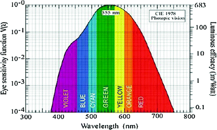
Eye sensitivity function, v(λ), and luminous efficacy of optical power, V(λ) is maximum at 555 nm [7]
Fig. 10.7 
CIE (x, y) chromaticity diagram [7]


In the standardization process, human eye sensitivity function (at wavelength 555 nm-green color) is taken as unity. For monochromatic light source, luminance efficacy (le) is of the order of eye sensitivity function, whereas for multicolor light source (e.g., white light source), le is calculated by integrating over all available wavelengths in the visible region. Three parameters are most important to define the color quality: (i) color rendering index (CRI), (ii) correlated color temperature, and (iii) chromaticity coordinate (CIE). The light source having good color rendering performance means it is emitting equivalent to a black body source at 3000–6000 K having CIE coordinates as (0.33, 0.33) corresponding to white light. Figure 10.7 shows chromaticity diagram where the boundaries represent plots of monochromatic light called spectrum loci. Area near the center of diagram is called Planckian Locus which represents plot of coordinates of black body radiation (1000–20,000 K). Most of the traditional sources emit between 2850 and 6500 K of Black Body (Table 10.2).
Some more important parameters:
-
1.
Luminance efficiency or power efficiency (ηp): Its units are candela per ampere (CdA−1) or Lumen per Watt (lmW−1). It is defined as Lumen output per input electrical power (Fig. 10.19b).
-
2.
Internal quantum efficiency (IQE): It is defined as number of photons generated inside the device per electron–hole pair injected into the device such that ηint = γηsΦs where γ is fraction of injected carriers that produce excitons and also known as charge balance factor, ηs is the fraction of singlet excitons, and Φs is fraction of energy released from material as light also called as quantum efficiency of fluorescence.
-
3.
External quantum efficiency (EQE): It is defined as total number of photons emitted from the device per electron–hole pair injected into the device such that η ext = R e η int where R e is the ratio of number of photons emitted into free space per second to number of photons emitted per second from the active layer. R e is also known as coupling efficiency.
-
4.
Life time: It is defined as average number of hours of operation in which the initial intensity drops to 50%.
Some typical examples of CPs giving different colors are given below
-
(i)
Orange—MEH-PPV
-
(ii)
Blue—PFO
A whole list of materials and list of venders (Sigma Aldrich, graphene supermarket, etc.) is available for OLED materials on various websites for different purposes like:
-
Charge transport and photosensitizing materials.
-
Electron transport and hole blocking materials.
-
Hole transport (HT) and hole injection layer (HIL) materials.
-
Host materials.
-
Light emitters and dopants.
-
Light-emitting polymers (LEPs).
White light is a suitable combination of red, green, and blue emitters/colors. In an inorganic LED, generally GaN or InGaN is used with different compositions (binary, ternary, and quaternary materials) and phosphors like Ce:YAG is used for color tuning which also depends upon the thickness and concentration of phosphor layers, and proper color mixing will give white light. For this purpose, multilayers are used and a typical example for obtaining white light OLED/PLED is shown in Fig. 10.8.

Multilayer structure of a typical WOLED/WPLED
New materials are being synthesized in various research and development laboratories all over the world to get cheaper, efficient, and long-life OLEDs.
In the following section, we will summarize some general and serious technology-based drawbacks of OLEDs and their possible solutions:
-
1.
Charge injection barriers at the interfaces of emissive materials can be reduced by having materials with suitable (closely matched) HOMO and LUMO levels.
-
2.
Lot of organic material waste can be avoided by precise control of parameters like thickness and composition of various layers.
-
3.
In spin coating for multilayer structure, generally it becomes difficult; it is difficult to coat one layer over other due to common solvent problem which may result in washing away the previous layer. Float lifting technique has been used to do away with this problem [7].
-
4.
Control of recombination zone location (which affects the CIE coordinates and efficiency) can be taken care of by incorporation of HTL, ETL, EBL, HBL; but sometimes they may result in increase in complexity.
-
5.
High operating voltage due to thick profile of various stacked organic layer is undesirable, therefore one needs to optimize the thickness of the layers.
-
6.
To enhance the contribution of triplet excitons toward radiative emission, one may use heavy metal elements which increase spin orbit coupling and enhance spin flip leading to more radiative decay. The other possible solution is use of phosphorent red and green dyes as guest to harvest/utilize triplet excitons [18, 19] by self-trapping mechanism.
-
7.
For better morphology, one has to optimize very carefully parameters like concentration of solution, spin duration, spin speed, annealing temperature, and annealing duration.
For color tuning, one needs optimized concentration of dopants or blending of two or more polymers [20, 21]. Further for emission, the energy transfer should be very fast and the materials should have appropriate concentration. For a white PLED, doping ratio of blue > green > red is required and carefully balanced.
The other possibilities are to use conducting polymer as host material and red/green phosphorent dyes as guest material (Fig. 10.9). Choice of right material has been a challenge as explained below:

Triplet energy levels of Ir(mppy)3 and Ir(piq)2(acac) with a CBP as HOST (b) PFO as HOST
The problem that can be noticed in (Fig. 10.9b) is that the triplet excitons energy level of blue-color emitting polymer, say PFO is well below that of green phosphorent dye, and therefore, the energy cannot be transferred from PFO to green dye. But at the same time since the red phosphorent dye has triplet excitons level lower than blue CP (blue color CP at 2.15 eV [22] and red at 2.0 eV [23]), the triplet energy may easily be transferred to red dye. Now that the problem has partly been solved by identifying materials for blue (CP PFO) and red color (dye–Ir (piq)2acac), the remaining is selection of a suitable green dye to complete RGB. Literature survey shows that a green phosphorent dye Ir (mppy)3 or [Iridum (III) tris (2-(4-tolyl) Pyridinato-NC2 is available. It has been shown by Devinder et al. [24] that even if host material is a suitable polymer (say PFO), the green dye can produce EL using self-trapping mechanism. The self-trapping mechanism (STM) and excitons formation has been shown in Fig. 10.10.

Favorable HOMO and LUMO levels of the guest material for self-trapping
The recovery condition is that for STM the LUMO level of green dye should be well below the LUMO level of host CP while HOMO level should be well above. The electrons injected from cathode and holes from anode (during biasing) get trapped in LUMO and HOMO of guest, respectively, and excitons is formed in dye itself. These excitons can decay radiatively and produce EL in green region and thus all the colors required for WOLED can be obtained. For efficient WOLED device, there is a need to optimize the concentration of RGB components so that their proper combination emits white EL.
To understand the experimental technique used to fabricate OLED, first we will discuss a typical structure for blue and green components [PFO + Ir (mppy)3] as shown in Fig. 10.11. For full RGB, red dye can be added in the active layer in the optimized composition to obtain WOLED.

A typical structure for OLED
The material used are PFO, Ir (mppy)3, chlorobenzene, ITO/glass substrate (anode), PEDOT:PSS, aluminum, and LiF (cathode). Following steps are used:
First of all, solutions of PFO and Ir (mppy)3 are made in chlorobenzene keeping PFO concentration constant as 10 mg/ml and varying dye concentration from 0 to 15 w/w%. The solutions are ultrasonicated and divided into two parts.
-
1.
In the first part, PFO and IR (mppy)3 composite films are spin coated on glass substrate for optical measurements (Absorption and PL).
-
2.
While the other part is kept for device fabrication on patterned ITO-coated glass having sheet resistance of ~15 Ω/□. Here ITO is used as anode. Over this substrate, a PEDOT:PSS layer (HTL) is spin coated keeping spin rate as 4000 rpm for 20 s. The samples are baked and dried in vacuum oven at 100 °C for ~1 h. Over this, an active (emissive) layer of PFO + Ir(mppy)3 having different concentration of Ir(mppy)3 is spin coated at spin rate of 2000 rpm for 30 s. These structures are annealed at 55 °C for 2 h. Finally, the Al contacts of 100 nm thickness are vacuum evaporated on the emissive layer as shown in Fig. 10.11.
Results of absorption and PL studies have been shown in Fig. 10.12a, b, respectively.

a Absorption spectrum of Ir(mppy)3 (normalized) and PFO (normalized). b PL spectra of the [PFO + Ir(mppy)3 (0–12%)] composite films (excitation wavelength 328 nm)
All the absorption and PL curves are normalized. The absorption spectra of PFO and phosphorent dye in p-xylene are shown in Fig. 10.12a. The minimum absorption of Ir(mppy)3 is at 328 nm and it serves as excitation wavelength in the PL studies. Normalized PL spectra Fig. 10.12b shows that there is no significant emission in green region even at high doping concentrations which means that the entire singlet excitons energy is used to produce blue PL and there is absolutely no transfer of singlet excitonic energy from PFO to green phosphorent dye no matter what concentration of dye was taken in the given range. PL studies on PFO show that peak emission of PFO is about 30 times higher as compared to Ir(mppy)3. In other words, green dye emits very weak PL as compared to PFO (for excitation wavelength of 328 nm). There may be some possibility of FRET but it is very insignificant.
The studies on effect of dye concentration in EL spectra of PLED having emissive layer of PFO + Ir(mppy)3 composite indicate that with increase in green concentration, green emission goes on increasing. When the concentration of green dye ≥ 6%, the green wavelength region overshoots the blue region. This is not due to transfer of energy from PFO to dye because the dye has higher triplet level than PFO.
And therefore the EL observed in green region Fig. 10.13 along with that of blue is due to the self-trapping mechanism (described earlier) and the probability of charge trapping increases with increase in green dye concentration in the present typical case Fig. 10.14.

EL spectra of the PLEDs fabricated using [PFO + (Ir(mppy)3 (0–12%)] composite films as the active emissive layers (A fixed current density of 50 mA/cm2 is used to drive all the diodes) [22]

Energy level diagram for the PFO/Ir(mppy)3 composites
Self-trapping of electron will take place from LUMO of PFO to LUMO of Ir(mppy)3, and self-trapping of holes takes place from HOMO of PFO to HOMO of Ir(mppy)3—both to make excitons which decay radiatively. Figure 10.15 shows the effect of dye concentration on the J–V characteristics. Initially up to 10% of the dye concentration the turn-on voltage increases and then starts decreasing slightly as the dye concentration increase from 10 to 12%.

J–V characteristics of the PLEDs fabricated using [PFO + Ir(mppy)3 (0–12%)] composite films as active emissive layers [22]
This may happen due to high concentration of guest molecules where the guest molecules come closer to form channel of charge carriers resulting in reduction of turn-on voltage. Finally, PLED parameters can be optimized and color tuning is possible by varying parameters like the thickness of the doped layer and dopant concentration. To get proper color coordinates [CIE (0.33, 0.33)], there is a need of optimization of concentration of various dopants. Actually as per Fig. 10.9b, it can be noticed that red dye can efficiently use triplet excitons because its triplet level is well below the PFO. Figure 10.16 is self-explanatory where normalized absorption and PL have been plotted as function of wavelength.

Figure showing overlap between absorption (ABS) spectrum of red dye (R) and photoluminescence (PL) spectra of green dye (G) and PFO (B)
Figure 10.16 exhibits the possibility of Forster Resonance Energy Transfer (FRET), where energy transfer is possible because of overlap of absorption of donor and emission of acceptor dye. It is a distance-dependent phenomenon, i.e., distance between donor and acceptor molecule which is order of few nms and it occurs primarily due to resonance of acceptor dipole with donor dipole. The concentrations of various RGB components need to be optimized carefully. The concentration of red dye is kept lowest of the three constituents as it is most effective and gets excited by charge trapping. FRET and self-trapping phenomenons are true for green dyes also. Some bioelectric materials like salmon DNA [25, 26] have been used successfully to improve the performance of MEH-PPV and PFO-based polymer LEDs.
As mentioned earlier, the sDNA-CTMA complex incorporated in WPLED at suitable position (Fig. 10.17) acts as electron blocking layer and enhances the performance of bio-WPLED. It helps in maintaining the balance of charge carriers by preventing electron from slipping out of recombination region, thereby increasing the probability of recombination of electrons and holes in the emissive layer. Figure 10.17 is self-explanatory. If we look at various HUMO and LUMO levels of different constituents, it can be noticed that DNA-CTMA complex due to its low LUMO level (0.9 eV) blocks efficiently electrons from going out of the emissive layer. The energy level of red dye ensures charge trapping in the dye because its LUMO level (3.2 eV) is well below that of PFO and HOMO level is well above that of PFO (5.2 eV).

Energy level diagram for the bio-WPLED fabricated
10.5 Fabrication Steps of Bio-WPLED [7]
Blue-emitting conducting polymer PFO was dissolved in chlorobenzene keeping the concentration as 10 mg/ml. To this solution, green [Ir(mppy)3] and red [(Ir(piq)2(acac))] phosphorescent dyes were added in concentration 0.8 and 0.2% w/w, respectively. These concentrations of the solutes were obtained after series of experiments by varying the dye concentrations in the host PFO so as to obtain best possible EL spectrum. The solution was homogenized using an ultrasonicator. This solution was spin coated on a patterned ITO-coated glass (having sheet resistance ~15 Ω/□), keeping the spin rate 2000 rpm for 30 s. The thickness of the film was measured with the help of talystep and is found to be 220 ± 10% nm (Figs. 10.18 and 10.19).

L–J–V characteristics for the bio-WPLED fabricated

Luminous and power efficiencies for the Bio-WPLED as a function of a luminance; b current density
The resistivity of the ITO substrate is very crucial for the device. If the resistivity is too high, the device current is likely to be very low and the turn-on voltage for the device will be high. On the other hand, if the resistivity is too low, the device is likely to be shunted. A resistivity of 15–20 Ω/□ has been found to be most appropriate by most of the workers for fabrication of LED structures. The ITO-coated glass substrates have to be clearly degreased, otherwise not only the emitted light will be obstructed but also spin-coated films will not stick and be non-uniform. Therefore, the substrate was first cleaned in an ultrasonic solvent bath for 10–20 min and then dried in a heating chamber at a temperature of ~50 °C for 2 h. The morphology of the film must be improved during fabrication. For this purpose, the concentration of PFO in chlorobenzene has been optimized. If the concentration of the solute is too high, the morphology will be poor due to kinks and overlapping of the chains. On the other hand, if the concentration of the solute is too low, the luminescence intensity will be poor. Before coating the emissive layer, a PEDOT:PSS layer is spin coated on the ITO. This layer acts as HTL and also smoothen the uneven surface of the ITO. A thin layer of DNA-CTMA complex was also coated on the PEDOT:PSS layer to act as an EBL. A buffer layer of LiF 10 nm thick is vacuum evaporated on the active layer, which reduces the potential barrier at the polymer/Al interface. The LiF layer also prevents the diffusion of Al atoms into the emissive layer during vacuum evaporation of cathode contact. On the buffer layer, Al cathode contacts of 100 nm thick are vacuum evaporated at a rate of 0.6 nm/s. A shadow mask was used for the deposition of the cathode resulting in the devices area of 2 mm × 2 mm.
10.6 Characteristics of Laboratory Made Prototype Typical Device
The turn-on voltage is quite high about 20–21 V, and the maximum luminescence is of the order of 350 Cdm−2 at bias voltage of 34 V as reported by us [26]. The luminous and power efficiency are reported as 0.86 CdA−1 and 0.12 lmW−1, respectively. There is a need to reduce the turn-on voltage. The color quality of bio-WPLED is also important. For a typical device fabricated by Madhwal et al. [21], all primary peaks start becoming significant beyond 25 V and become stable around 32–34 V as shown in Fig. 10.20.

EL spectra and corresponding CIE coordinates for the bio-WPLED [21]. Inset Sample picture and the working WPLED
The CIE obtained is (0.30, 0.34) which is close to the pure white light (0.33, 0.33). All these values are approximate and vary slightly with chemical and physical parameters like concentration, type of solvent, and the process involved. It’s important to note that the concentration of red dye has to be optimized carefully because beyond a certain value (say 2 w/w % for a typical case) the dye molecule start segregating and making clusters which is not desirable (Fig. 10.21).

Confocal micrograph of the films: red dye doped in PFO [a 2%, b 5%, c 15%] confocal (LSM 510, Carl Zeiss, Germany)
The general chromaticity diagram is shown in Fig. 10.22. To further increase the efficiency, it is necessary to revisit the parameters which adversely affect the performance of LED. Some of the major problems have already been discussed in this chapter viz. charge imbalance, loss of triplet excitons, morphology of the thin film, poor mobility of electron and holes in CPs, excitons quenching near the metal electrodes, the presence of metal contamination into CP after cathode evaporation [27]. Chance et al. [28] have shown that metals like Ca diffuse from cathode into the emissive polymer and form high number of quenching centers near the cathode. Further due to proximity of metal electrode to the polymer layer, there is a possibility of a short distance non-radiative energy transfer from the fluorescent layer to metal.

Chromaticity diagram for the bio-WPLED Fabricated showing CIE coordinates at different bias voltages
Use of suitable ETL may be one of the possible solutions in order to improve the efficiency of the device. DNA-CTMA EBL alone would not be able to enhance the efficiency of WPLED to sufficient extent, and suitable ETL can enhance mobility of electron and helps in shifting the recombination zone away from metal electrode. As a result, the exciton formation will take place away from the metal electrode reducing the possibility of their quenching by metal electrode. Single-walled carbon nanotubes (SWNT) have been identified as excellent electron transporting material (ETL). It has been shown by Singh et al. [29, 30] that incorporation of CNT in CPs (concentration of 5 w/w%) matrix enhances its conductivity by 5–6 order of magnitude by making an efficient network therefore for a typical MEHPPV-SWCNT composite film-based LED the luminance increased approximately by 5 times [31]. It has been shown that incorporation of ETL not only improves charge balance between the electron and holes but also shifts the recombination zone away from the metal electrode thus, resulting in a significant improvement in luminance of the device. Therefore, the use of SWNT (ETL) in conjunction with DNA-CTMA complex (EBL) which increases the luminous efficiency of this multilayered (MEHPPV-SWNT) composite with EBL by about 20 times [7]. Some worker have suggested the use of Alq3 as suitable ETL because it has excellent film formability and low ionization potential (5.7 eV) making it an appropriate candidate for blocking holes and transporting electrons in the emissive layer. But the two main problem with Alq3 is that since it is a green emitter, it interferes with the emission spectra of LED and due to lower molecular weight it cannot be spin coated (because it is not soluble inorganic solvent) and needs relatively expensive vacuum evaporation technique which is not commercially viable. Therefore, Alq3 was not used. In the case discussed above, MEHPPV-SWNT composite layer for ETL was casted over emissive layer using a special technique where extreme care was taken. This technique prohibited washing away of one layer (due to same solvent) when other layer was spin coated over it. This technique has been discussed below for a typical structure shown in Fig. 10.23.

MEH-PPV-SWCNT composite bio-LED
Here MEH-PPV-SWCNT composite has been used as ETL over the emissive layer of (MEH-PPV). Since both, emissive layer and ETL (MEHPPV-SWCNT composite) had the common organic solvent, they both dissolve in common organic solvent when one layer is spin cast over the other (here thin film of MEHPPV-SWCNT composite is spin cast over MEH-PPV emissive), the MEH-PPV layer is washed out. This is highly undesirable. Therefore, to fabricate the ETL over emissive layer, float lift technique is used. In this technique, first of all MEH-PPV/DNA-CTMA complex/PEDOT:PSS/ITO structure is made by spin cast technique. Now ethylene glycol is taken in a petri dish. Over this, a few drops of MEH-PPV-SWCNT composite solution are cast which spreads uniformly over highly viscous glycol and floats over it. Now the already made dried structure MEH-PPV/DNA-CTMA complex/PEDOT:PSS/ITO is placed over the thin dried layer of MEH-PPV-SWCNT (ETL) floating on ethylene glycol for one minute carefully. The floating film MEH-PPV-SWCNT will adhere itself to MEH-PPV emission layer due to non-sticking nature of ethylene glycol. The samples are then dried in vacuum oven to remove the residual ethylene glycol. Al contact (cathode) is vacuum coated over this ETL. Now the device is ready for characterization.
A comparison of LED characteristics (Current density J vs. Bias voltage and Luminescence vs. J) with and without ETL has been shown for a typical lab made device in Figs. 10.24 and 10.25. Significant improvement is observed mainly due to the fact that SWCNT improves/provides high mobility to the electrons and there is an improvement in the injection of the charge carriers. Some workers have used ZnO nanorods (NR) for increasing the emission of MEH-PPV for a typical structure shown in Fig. 10.26a, b [32]

Current density—bias voltage characteristics of SL and TL devices

Luminance as a function of current density for the TL and SL devices

a incorporation of ZnO nanorods in single layer structure. b final device structure
In this structure, ZnO NR were grown by electro-chemical method over ITO (15 Ω/□), after that LiF (10 nm) and Al contact were vacuum evaporated. The overall thickness of the device was 900 nm. A comparison of J versus V and luminescence versus J with and without ZnO nanorods is shown in Fig. 10.27a, b which indicate a significant enhancement in the performance of LED. The turn-on voltage decreases and luminance increases by incorporation of ZnO NRs.

a J–V characteristics of MEH-PPV-based PLEDs. b luminance characteristics for MEH-PPV PLEDs with and without ZnO nanorods
The reason is that ZnO NRs unwind the polymer chains and connect them in such a way that an alternate mechanism for charge transfer is obtained besides already present normal hopping process. Another improved structure is shown in Fig. 10.28.

Schematic of ZnO nanorods-based UV LED
Here there is an enhancement in UV emission due to Burstein Moss effect [33, 34]. Vertically aligned ZnO NRs can also be fabricated cost effectively by hydrothermal method with the help of seed layer [35]. These LEDs have been proposed to be used both for UV LED as well as UV lasers.
10.7 Conclusion
Conducting polymers and based devices is one of the hot areas of research where efforts are being made all over the world to synthesize new polymer materials to achieve higher mobility (at least one to two orders of magnitude higher) of the charge carriers so as to obtain higher efficiency and lower cost. There is a need to address the stability issues besides developing low-power consuming devices. The future of the conducting polymer-based electronics is very promising, and in the coming days, these materials may replace some of the conventional materials used in the present day electronic devices.
The prospects of OLEDs in industry are very bright. Commercialization of these OLEDs in displays, lighting, TV screens, etc., is in high progress.
References
Times of India page 21 ‘Energy conservation’ dated 28 Feb. 2009, Saturday
Lucifer™ Lights Pvt. Ltd. (www.ledindia.com)
H.S. Kang, M.S. Kim, K.T. Park, K.M. Kim, T.H. Lee et al., Curr. Appl. Phys. 1, 443 (2001)
C. Ulbricht, B. Beatrice et al., Adv. Mater. 21, 4418 (2009)
B.W. D’Andrade, S.R. Forrest, Adv. Mater. 16, 1585 (2004)
H. Youn, M. Yang, Appl. Phys. Lett. 97, 243302 (2010)
D. Madhwal, in Development of Conducting Polymer Based White Light Emitting Diode. Ph. D. thesis, University of Delhi, p. 5
S.H. Jin, S.Y. Kang, I.S. Yeom, J.Y. Kim, S.H. Park, K. Lee et al., Chem. Mater. 14, 5090 (2002)
C.C. Huang, H.F. Meng, G.K. Ho, C.H. Chen, C.S. Hsu, J.H. Huang et al., Appl. Phys. Lett. 84, 1195 (2004)
C. Ego, D. Marsitzky, S. Becker, J. Zhang, A.C. Grimsdale, K. Muellen et al., J. Am. Chem. Soc. 125, 437 (2003)
A.B. Kaiser, Rep. Prog. Phys. 64, 1 (2001)
R.H. Friend et al., Nature 397, 121 (1999)
H. Burroughs, D.D.C. Bradley, A.R. Brown, R.H. Friend, Nature 347, 539 (1990)
A.R. Brown, D.D.C. Bradley, P.L. Burns, J.H. Burroughes, R.H. Friend, N. Greenham, A.B. Holmes, A. Kraft, Appl. Phys. Lett. 61, 2793 (1992)
en.wikipedia.org/wiki/Lighting, “comparison of various light sources”
R. Song, Y. Dduan, S. Chen, Y. Zhao, J. Hou, S. Liu, Semic. Sci. Tech. 22, 728 (2007)
J.H. Seo, J.H. Seo, J.H. Park, Y.K. Kim, J.H. Kim, G.W. Hyung, Appl. Phys. Lett. 90, 3507 (2007)
H.A. Al Attar, A.P. Monkman, M. Tavasli, S. Bettington, M.R. Bryce, Appl. Phys. Lett. 86, 121101 (2005)
D. Madhwal, S.S. Rait, A. Kumar, A. Verma, K. Tada, M. Onoda, P.K. Bhatnagar, P.C. Mathur, J. Mater. Sci. 45, 3300 (2010)
U. Scherf, D. Neher, Advances in polymer science. Polyfluorenes 212
Y. Lyu, J. Kwak, W.S. Jeon, Y. Byun, H.S. Lee, D. Kim, C. Lee, K. Char, Adv. Funct. Mater. 19, 420 (2009)
D. Madhwal, S.S. Rait, A. Verma, A. Kumar, M. Onoda, P.K. Bhatnagar, P.C. Mathur, PhysicaScripta 81, 0657 (2010)
J.A. Hagen, W. Li, A.J. Steck, J.G. Grote, Appl. Phys. Lett. 88, 171109 (2006)
D. Madhwal, S.S. Rait, A. Verma, A. Kumar, P.K. Bhatnagar, P.C. Mathur, M. Onoda, J. Lumin. 130, 331 (2010)
W.R. Salaneck et al., The metal on polymer interface in polymer light emitting diodes. Adv. Mater. 8, 48 (1996)
R.R. Chance, A. Prock, R. Sibey, Comments on the classical theory of energy transfer. J. Chem. Phys. 62, 2245 (1975)
I. Singh, P.K. Bhatnagar, P.C. Mathur, I. Kaur, L.M. Bharadwaj, R. Pandey, Carbon 46, 1141 (2008)
I. Singh, A. Verma, I. Kaur, L.M. Bharadwaj, V. Bhatia, V.K. Jain, C.S. Bhatia, P.K. Bhatnagar, P.C. Mathur. J. Polym. Sci. Part B: Polym. Phys. 48, 89 (2010)
I. Singh, D. Madhwal, A. Verma, A. Kumar, S.S. Rait, I. Kaur, L.M. Bharadwaj, C.S. Bhatia, P.K. Bhatnagar, P.C. Mathur, J. Lumin. 130, 2157 (2010)
R. Bhardwaj, in Development and Characterization of Conducting Polymer/ZnO Based Bio-Light Emitting Diode. Ph. D. thesis, University of Delhi (2013)
E. Burstein. Phys. Rev. 93, 632 (954)
T.S. Moss, Proc. Phys. Soc. 67, 775 (1954)
K. Gautam, I. Singh, P.K. Bhatnagar, K. Rao Peta, Superlattices Microstruct. 93, 101–108 (2016)
Author information
Authors and Affiliations
Corresponding author
Editor information
Editors and Affiliations
Rights and permissions
Copyright information
© 2018 Springer Nature Singapore Pte Ltd.
About this chapter
Cite this chapter
Bhatnagar, P.K. (2018). Organic Light-Emitting Diodes—A Review. In: Khan, Z. (eds) Nanomaterials and Their Applications. Advanced Structured Materials, vol 84. Springer, Singapore. https://doi.org/10.1007/978-981-10-6214-8_10
Download citation
DOI: https://doi.org/10.1007/978-981-10-6214-8_10
Published:
Publisher Name: Springer, Singapore
Print ISBN: 978-981-10-6213-1
Online ISBN: 978-981-10-6214-8
eBook Packages: Chemistry and Materials ScienceChemistry and Material Science (R0)