
Abstract
Until the mid-1980s, the nMOS silicon-gate process was the most commonly used process for MOS LSI and VLSI circuits. However, nearly all modern VLSI and memory circuits are made in CMOS processes. CMOS circuits are explained in Chap. 4; the technology used for their manufacture is discussed in this chapter.
Access provided by CONRICYT-eBooks. Download chapter PDF
Keywords
These keywords were added by machine and not by the authors. This process is experimental and the keywords may be updated as the learning algorithm improves.
3.1 Introduction
Until the mid-1980s, the nMOS silicon-gate process was the most commonly used process for MOS LSI and VLSI circuits. However, nearly all modern VLSI and memory circuits are made in CMOS processes. CMOS circuits are explained in Chap. 4; the technology used for their manufacture is discussed in this chapter.
Modern nanometer CMOS processes, with channel lengths below 30 nm, have emerged from the numerous manufacturing processes which have evolved since the introduction of the MOS transistor in integrated circuits. Differences between the processes were mainly characterised by the following features:
-
The minimum feature sizes that can be produced.
-
The gate oxide thickness.
-
The number of interconnection levels.
-
The type of substrate material. Alternatives include n-type and p-type, high-resistive or low-resistive, bulk silicon, epitaxial or SOI wafers.
-
The choice of the gate material. Initially, the gate material was the aluminium implied in the acronym MOS (Metal Oxide Semiconductor). Molybdenum has also been used. From 6 μm until and including 120 nm MOS processes and above, however, nearly all use polycrystalline silicon (polysilicon) as gate material. One of the main reasons is that a polysilicon gate facilitates the creation of self-aligned source and drain areas. Another reason for using polysilicon as gate material is that it allows accurate control of the formation of the gate oxide. From 90 nm onwards, a stack of W-WN-polysilicon and SiOxNy is used. A combination of a metal gate with high-ε dielectrics is first introduced in the 45 nm node by Intel. Other companies have introduced high-ε, metal gate devices in their 32 or 28 nm CMOS nodes.
-
The method to isolate transistors. Conventional CMOS processes used the so-called LOCOS isolation while most of today’s processes use Shallow-Trench Isolation (STI), see Sect. 3.4.
-
The type of transistors used: nMOS, pMOS, enhancement and/or depletion, etc.
Many of the transistor parameters, in terms of performance, power consumption, and reliability, are determined by the substrate that is used as starting material. A short summary on the properties and use of the different substrate materials will therefore be presented first.
Modern manufacturing processes consist of numerous photolithographic, etching, oxidation, deposition, implantation, diffusion and planarisation steps. These steps are frequently repeated throughout the process and they currently may exceed a thousand steps. The IC fabrication discussion starts with a brief description of each step. Most processes use masks to define the required patterns in all or most of the IC diffusion and interconnect layers. Modern CMOS manufacturing processes use between 25 and 50 masks. However, the initial discussion of IC manufacturing processes in this chapter focuses on a basic nMOS process with just five masks.
Subsequently, a basic CMOS process flow is briefly examined. Fundamental differences between various CMOS processes are then highlighted.
Finally, a sample nanometer CMOS process is explained. Many of the associated additional processing steps are an extension of those in the basic CMOS process flow. Therefore, only the most fundamental deviations from the conventional steps are explained. The quality and reliability of packaged dies are important issues in the IC manufacture industry. An insight into the associated tests is included in Chap. 10
3.2 Different Substrates (Wafers) as Starting Material
To create silicon wafers, first pure silicon is heated at temperatures up to 1500 ∘C in a huge furnace. Then a seed of single silicon crystal is mounted on a shaft and is dipped into the molten silicon. This seed is then slowly rotated and raised upwards out of the melt just fast enough to pull the molten silicon with it by cohesion, thereby physically growing the silicon crystal. In this so-called Czochralski process the crystal growth is a continuous process of forming new thin films of the silicon melt on the bottom of the cooled previous films, roughly at about 20 mm an hour. The diameter of the grown mono crystalline silicon bar (also called ingot ) varies over the length and a grinder is used to create a bar (Fig. 3.1) with a homogeneous diameter, which can be more than 300 mm.


A 300 mm silicon ingot from which 300 mm wafers are sawn (Courtesy of Smartalix)
A 300 mm crystal ingot can be as long as 2 m and may weight several hundred kilograms. Next, wafers are sawn by a diamond-coated saw. Because the transistors are fabricated close to the silicon surface, their performance and reliability are very much dependent on the flatness and crystal integrity of the silicon surface. Theoretically, for good MOS transistor operation, the wafers could be as thin as a micron, but with this thickness, a wafer would easily break during handling. Therefore most wafers have a thickness between 400 μm and 1 mm.
A very critical element in the operation of an integrated circuit is the electrical isolation between the individual devices. Unintended electrical interference can dramatically affect their performance. Smaller minimum feature sizes reduce the distance between devices and increase their sensitivity at the same time. An important factor in the isolation properties is the substrate on which the devices are built. In all discussions, so far, we have assumed a bulk silicon substrate (wafer) as the starting material for our (C)MOS processes. However, CMOS technologies used epitaxial wafers in the past, while most advanced processes use normal bulk-silicon wafers, while several high-performance microprocessors are made on SOI wafers. The properties and use of these substrates (wafers) will be discussed next.
3.2.1 Wafer Sizes
From an economical perspective, larger wafers have led to reduced IC manufacturing costs. This rule drove the wafer diameter from about 1 inch ( ≈ 25 mm), about four decades ago, to 12 inches ( = 300 mm) today. This has put severe pressure on maintaining the wafer flatness, its resistivity and low crystal defect density homogeneous across a rapidly increasing wafer area. However, the introduction of a new wafer diameter generation requires a huge amount of development costs. This has put the transition from 300 mm to 450 mm wafers on hold and it still needs billions of dollars investment before volume production can take off. In this respect, big semiconductor houses such as Intel, TSMC, IBM, Samsung and Globalfoundries have joined R&D forces [1] in a five-company consortium (G450C), in a partnership with the College of Nanoscale Science and Engineering at the State University of New York, to develop the next generation wafer technology. Figure 3.2 shows the 300 mm fab cost evolution as a function of the feature size.


300 mm logic fab cost as a function of feature size (Courtesy: Globalfoundries)
Upgrading a 300 mm fab from 32 nm to 22 nm would cost around $2B. However, the transition from 300 mm production to 450 mm production would require about $7B, because all fab equipment must be upgraded. Another disadvantage is the more complex fabrication of the 450 mm diameter silicon bar (crystal ingot) . It will be three times heavier (around 1000 kg). This, combined with the much larger time required for cooling, will almost double the process time. As stated before, the development of 450 mm technology is almost completely put on hold [2]. Therefore, volume production is not expected before 2022 [1], if it will ever happen.
3.2.2 Standard CMOS Epi
Epitaxial wafers (epitaxial from Greek: epi = above; taxis = to arrange) consist of a thin, mono-crystalline silicon layer grown on the polished surface of a bulk silicon substrate (www.memc.com). This so-called epi layer is defined to meet the specific requirements of the devices in terms of performance, isolation and reliability. This layer must be free of surface imperfections to guarantee a low defect density and limit the number of device failures. Since the carriers in a transistor channel only travel in the surface region of the device, the epi layer thickness is only defined by the transistor architecture (source/drain and STI depths) and ranges from one to a few microns. Usually the total wafer thickness is typically 750 μm, but may range between 400 μm and 1 mm, depending on the wafer size and technology node. It means that the top epi layer forms only less than 1% of the total wafer and that the major part of the wafer mainly serves as a substrate carrier for the ICs made on it.
Although the resistance of this substrate hardly affects the performance of digital circuits it has influence on the robustness of the ICs built on it. Most conventional CMOS processes, including the 180 nm node, use/used low-resistivity (5–10 m\(\Omega\) cm at doping levels between 5⋅ 1018 and 1⋅ 1019 atoms/cm3) wafers, in order to reduce the chance of latch-up occurrence (see Chap. 9). With reducing supply voltages the chance for triggering the parasitic transistor to initiate latch-up is also diminishing. This, combined with the increasing integration of GHz RF functions, has made the use of high-resistivity (10–50 \(\Omega\) cm at doping levels between 1⋅ 1015 and 1. 5⋅ 1015 atoms/cm3) substrates very popular from the 120 nm CMOS node onwards. It leads to performance increase of passive components, such as inductors, but also to a better electrical isolation between the noisy digital circuits and the sensitive RF and analog ones (less substrate noise; Chap. 9).
Because the full device operation occurs within this thin top epi layer, it puts severe demands on the homogeneity of the layer thickness, of the resistivity and of the crystal defectivity. When growing single crystal silicon, either for creating bulk silicon wafers or for creating thin epi layers, a few typical defects in the silicon may show up. Point defects may originate from single empty locations (vacancies) in the monocrystalline atomic structure (Fig. 3.3), while micro defects or crystal-oriented particles (COP) can be the result of a cluster of voids.


Defects in silicon (Source: MEMC)
Interstitials are atoms located in between the atoms of the crystal, while dislocations may be caused by clusters of interstitials. The average atomic spacing is also dependent on the covalent atomic radius of the specific material: Silicon (Si) 1.17 Å, Boron (B) 0.88 Å, Phosphorous (P) 1.10 Å, Arsenic (As) 1.18 Å, Stibnite (Sn) 1.36 Å. So, B is a smaller atom than Si. Doping Si with B (or P) reduces the average atomic spacing of the Si crystal. Another result of this is that the average atomic spacing in the p− epi layer is larger than that in the p+ substrate, because the substrate contains a higher concentration of smaller atoms. Large differences in the atomic spacing of different layers may lead to so-called misfit dislocations. To prevent misfit dislocations in a thin epi layer on a resistive substrate a simple rule of thumb is applied [4, 5]:
-
epi thickness in μm ≤ substrate resistivity in m \(\Omega\)
Today, the quality of the Czochralski process of creating the silicon has improved such that it results in extremely pure (purity of 99.9999999%) mono-crystalline silicon, which is almost defect free. The defectivity level of these bulk silicon wafers is certainly comparable to, or even better than that of wafers with an epitaxial layer. It is no longer needed to compensate bulk defects. Some semiconductor applications, however, still require epitaxial wafers, but then it is for better control and adjustment of the dopant and the resistivity of the layer.
These examples show that not all ICs can be made on the same substrate. The following subjects discuss substrates that enhance the device performance.
3.2.3 Crystalline Orientation of the Silicon Wafer
As discussed in Chap. 2, the effective mobility of the carriers in the channel has reduced dramatically over time, due to the continuous scaling of the transistors. Suppressing short-channel effects by increasing the channel doping has led to an increased density of charged impurity scattering sites, thereby reducing the mobility of the carriers in the channel. The intrinsic speed of a logic gate, in first approximation, is proportional to the mobility. Therefore, a lot of research is currently performed in a variety of ways to improve carrier mobility. In this respect also the crystalline orientation of the silicon substrate plays an important role.
Traditionally, CMOS has been fabricated on wafers with a (100) crystalline orientation, mainly due to the high electron mobility and low interface trap density. However, the pMOS transistors on this substrate suffer from a low mobility. By moving away from the (100) orientation, electron mobility is degraded, while hole mobility is improved. Compared to a traditional (100) wafer, a (110) wafer can show hole mobility improvements up to 30% in practice, while electron mobility may have degraded by about 5–10%. An optimum technology, with a much better balance between nMOS and pMOS device performance would be a hybrid-orientation technology: the (100) plane for nMOSts and the (110) plane for the pMOSts [6, 7], see also Sect. 3.9.4.
If the pMOS channel is oriented along the < 100 > direction on a (100) wafer, its mobility and performance may be increased by about 15%, with almost no degradation of the nMOSt performance. Another advantage is that the pMOS transistor will also exhibit a reduced variability. This is only a minor change in the starting wafer, with no further consequences for the device technology and layout (Fig. 3.4).


(a ) traditional notch grinding and (b ) grinding the notch in the < 100 > direction (Source: MEMC)
The only difference is that the wafer flat alignment or notch is changed from the standard < 110 > direction to the < 100 > direction. Traditionally, the notch is cut during crystal grinding in the < 110 > direction (Fig. 3.4a). To orient the channel direction along < 100 > requires a crystal rotation of 45∘ to grind the notch in < 100 > direction (Fig. 3.4b). This orientation change is a low cost solution to enhance the pMOS device, logic gate and memory cell performance with no risk or consequences for the integration process. This wafer option is already in use in high volume production since the 120 nm node.
3.2.4 Silicon-on-Insulator (SOI)
Bulk-CMOS devices show relatively large source/drain capacitances. This can be avoided with the SOI-CMOS devices illustrated in Fig. 3.5. The complete isolation of nMOS and pMOS transistors associated with this process also completely removes the possibility of latch-up .


Cross section of a basic SOI-CMOS process
Neither the nMOS nor pMOS transistor channels require over-compensating impurity dopes. Very small body effects and source/drain capacitances are therefore possible for both types of transistor. In addition, the n+ and p+ source and drain regions do not have bottom junctions. Consequently, the parasitic capacitances are much less than those of the bulk-CMOS processes. This makes the SOI-CMOS process particularly suitable for high-speed and/or low-power circuits. Murphy’s law , however, ensures that there are also several disadvantages associated with SOI-CMOS processes. The absence of substrate diodes, for example, complicates the protection of inputs and outputs against the ESD pulses discussed in Chap. 9.
Sapphire was originally used as the isolating substrate in SOI-circuits, despite the fact that it is substantially more expensive than silicon. The SIMOX (‘Separation by IMplantation of OXygen’) process provides a cheap alternative for these silicon-on-sapphire or ‘SOS-CMOS’ processes. Several modern SOI-CMOS processes were based on SIMOX. These processes use a retrograde implantation of oxide atoms to obtain a highly concentrated oxygen layer beneath the surface of a bare silicon wafer. The resulting damage to the wafer’s crystalline structure is corrected in an annealing step. The result is shown in Fig. 3.6.


(a ) Cross section of a SIMOX wafer and (b ) SEM photograph of such a cross section
SIMOX wafers were delivered with a buried-oxide layer (BOX layer) (SiO2) varying from less than 20 nm to 150 nm, with a top silicon layer varying from less than 10 nm to 100 nm. This is done to reduce the consequences of damage on the wafer surface. Fully depleted devices can be realised by reducing the thickness of the top layer to below 50 nm, for example, during processing. An alternative to the SIMOX process flow to create SOI is the Smart Cut process flow (Fig. 3.7).


Smart-cut process flow (Source: SOITEC)
After the original wafer is first oxidised to create an isolating layer, H+ ions are implanted to form a ‘weak’ layer at a certain distance below the surface. The thickness of the top layer is determined by the implantation energy. Next the wafer is cleaned and bonded upside-down to another wafer for further handling. During the ‘smart cut’ step, the wafer is heated, such that the wafer is split exactly at the implanted weak H+ layer. The remaining part of the wafer is reused again as original wafer, or as carrier for a new SOI wafer, and the process cycle starts again. Finally, the SOI wafer needs an annealing step to recover the atomic structure, which was damaged during the implantation step. After a CMP planarisation step, the SOI wafer is ready. This smart-cut technology can be used for a wide range of SOI and BOX thickness.
In an SOI device with a thick top silicon layer (Fig. 3.8a), this layer can only become partially depleted (PD-SOI) during operation, showing such parasitic effects as the floating-body and Kink effect. A thin-body device ( < 50 nm) (Fig. 3.8b) will become fully depleted (FD-SOI) and does not show these effects.


Cross section of a (a ) partially depleted SOI device and (b ) a fully depleted SOI device
For advanced low-voltage CMOS ( ≤ 1 V) system-on-chip designs with digital, analogue and RF parts, SOI is expected to offer a better performance than bulk CMOS technology [9, 10]. SOI is said to deliver more speed at the same power consumption, or to consume less power at the same speed. Furthermore, SOI realises better isolation between digital, analogue and RF parts on the IC. Those circuits will therefore be less affected by substrate noise. Additionally an SOI transistor has lower parasitic capacitances and consequently exhibits a better RF performance. SOI devices are thermally insulated from the substrate by the buried-oxide layer. This leads to a substantial elevation of temperature (self-heating) within the SOI device, which consequently modifies the output IV-characteristics of the device, showing negative conductance. These effects, which are considerably larger in SOI than in bulk devices under similar conditions, must be taken into account by device technology engineers, model builders and designers. Since the body is isolated, SOI circuits show several advantages, compared to bulk-CMOS:
-
smaller junction capacitances
-
no deep well required (this is especially an advantage for FD-SOI)
-
less n+ to p+ spacing, due to absence of wells
-
significant reduction in substrate noise (questionable at high frequencies > 1.5 GHz)
-
no manifestation of latch-up
-
reduced soft-error rate (SER), because the electron-hole pairs generated in the substrate cannot reach the transistors
-
steeper subthreshold slope, which can be close to the theoretical limit of 63 mV/decade, compared to around 80 mV/decade for bulk CMOS devices
The future for planar partially depleted SOI devices is not completely clear. The relative performance benefit due to the smaller junction capacitances of SOI will gradually reduce because this advantage diminishes with scaling. Junction area capacitance decreases with the square of the scaling factor while gate and perimeter capacitances decrease only linearly. Next to this, the increasing impacts of interconnect capacitances and delays will also reduce the performance benefits of SOI.
For the 45 nm node most semiconductor manufacturers still use bulk CMOS as their main process technology. However, beyond this node, FD-SOI may become a good alternative to bulk-CMOS. Since the channel region is fully depleted, it largely eliminates the neutral body. It therefore hardly exhibits the floating-body, history and kink effects. Moreover, it is expected to show improved short-channel effects (SCE) and drain-induced barrier lowering (DIBL). FD-SOI requires a reduced channel-doping concentration, leading to a higher mobility and a much steeper subthreshold slope , which almost matches the ideal value of ≈ 63 mV/decade (Fig. 3.9), compared to the ≈ 80 mV/decade for a bulk-CMOS process.


Schematic illustration of current characteristics and subthreshold behaviour of bulk-CMOS and FD-SOI
The diagram shows that in an SOI process, a transistor may have a lower V T than in a bulk-CMOS process, while carrying the same subthreshold leakage current. This advantage can either be used for speed improvement, when running SOI at the same supply voltage as bulk-CMOS, or for power reduction, when running SOI at a lower supply voltage but at the same speed. FD-SOI allows sub-1V RF circuits, with improved F t and F max and reduced noise levels.
The transistors in such a nanometer FD-SOI process are fabricated in a thin film, with a thickness ≈ 5–20 nm on a box thickness between 5 and 50 nm [8]. Because the body between source and drain is fully depleted, the V T-spread in these devices is much less dominated by the doping levels. Instead, it now depends heavily on the film thickness, whose uniformity across an 8 inch or 12 inch wafer has become a major criterion in the success of FD-SOI. This uniformity is therefore likely to have a more global (inter-chip) than local (intra-chip) impact on the variability in device operation. Below the 22 nm node planar SOI devices are expected to show device current degradation due to ‘quantum confinement’ [11].
Many other alternative device and process options have been applied in technologies beyond the 45 nm node. A flavour of these technology options in both the devices and interconnects is presented in Sect. 3.9.4.
3.3 Lithography in MOS Processes
3.3.1 Lithography Basics
The integration of a circuit requires a translation of its specifications into a description of the layers necessary for IC manufacture. Usually, these layers are represented in a layout . The generation of such a layout is usually done via an interactive graphics display for handcrafted layouts, or by means of synthesis and place-and-route tools, as discussed in Chap. 7 Figure 3.10 shows an example of a complex IC containing several synthesised functional blocks.


Example of a complex signal processor chip, containing several existing IP cores with newly synthesised cores (Source: NXP Semiconductors)
A complete design is subjected to functional , electrical and layout design rule checks. If these checks prove satisfactory, then the layout is stored in a computer file (gds2 file). This database is now ready for tape-out . This term originates from the past when the complete database was loaded in gds2 format onto a magnetic tape. Tape-out is the final design description which will be used for manufacture. The first activity in the manufacturing process is the creation of the physical masks. A software program (post-processor) is used to convert this database to a series of commands. These commands control an Electron-Beam Pattern Generator (EBPG) or a Laser-Beam Pattern Generator (LBPG) , which creates an image of each mask on a photographic plate called a reticle (Fig. 3.11). Such a reticle contains a magnified copy of the mask patterns. The reticle pattern is thus demagnified as it passes through the projection optics. Usually a reticle contains four times the physical sizes of the patterns. The sizes of image field of 26 × 33 mm are the physical sizes on the wafer. On reticle level, these sizes are four times larger. The grey areas at the left and right side of the image field contain Barcodes, reticle ID and pre-alignment markers. The alignment markers consist of an X-mark and a Y-mark, respectively above and left from the image field. On the wafer they will become imaged in the scribe lanes, which are typically 40 μm wide to enable separation of the individual dies by mechanical sawing or laser cutting. For wafer alignment, about 16 X/Y pairs, distributed over the wafer, are being measured.


Schematic layout of a 4× reduction reticle for step and scan systems (Source: ASML)
During the printing process, often pellicles are used to protect the reticle from harmful particles. A pellicle is a very thin transparent membrane adhered to a metal frame, which keeps particles out of focus during the lithographic process, so it will not image onto the wafer and reduces the possibility of printing defects. Particularly with the introduction of 193 nm, the light transmission loss in the pellicles increases with the number of exposures, such that they frequently need to be replaced. The cost of a mask set is subject of discussion in Sect. 3.3.4.
Small feature sizes, such as currently required in deep-submicron ( < 0. 25 μm channel lengths) and nanometer ( < 100 nm) CMOS processes, are obtained by using reduction steppers or scanners. Current reduction steppers and scanners use four-to-one (4:1) reduction step-and-repeat or step-and-scan . A traditional step-and-repeat system only moves the wafer rapidly to the next die (or reticle field) position and holds while the whole reticle field is exposed during a single exposure. In a step-and-scan system, both the wafer and the reticle move synchronous in opposite directions at (four times) different speed controlled by a high-precision tracking system. It scans a narrow image field across the total reticle field. After the total field has been scanned, it steps to the next field position on the wafer. The reduction is achieved by means of a system of (very) complex lenses. Figure 3.12 shows a basic schematic of a generic optical projection system. In a real photolithographic system both the illuminator path (light source to reticle) and the projection path (reticle to wafer) consist of a couple of lenses.


Basic schematic of generic optical projection system
Limitations of these projection lithography techniques are not only determined by the wavelength λ of the applied light source and the Numerical Aperture NA. A stepper/scanner also needs to create clear, high-contrast images, while it must offer a sufficient depth of focus DOF to accommodate system and process-focus (height) variations which also lead to critical dimensions (CD) variation. The combination of a large number of metal layers and extremely large-area designs create significant topographies across these designs and put stringent demands to the DOF. Current CMP planarisation technology limits topology variations to below 40 nm.
The resolution of the resulting projections is limited by diffraction and also depends on the properties of the photo-resist. Better photo-resists allow smaller minimum feature sizes. There are two expressions, developed by Ernst Abbe around 1867, which describe the most important characteristics of a lithographic imaging system. Firstly, the feature size F ( ≡ half pitch for memories, often also referred to as critical dimension (CD) ), which refers to the minimum width of the printed patterns, is defined by:
where k 1 is a constant, which is a function of the resist, the mask, illumination and resolution enhancement techniques (RET) , which will be discussed later. With ‘conventional’ three-beam imaging , where only the zero- (0) and first-diffraction order rays ( − 1 and + 1) pass the lens, the value of k 1 is restricted to: \(k_{1} \geq \frac{1} {2}\). When phase shift masks (PSM) or off-axis illumination (both techniques are explained later in this section) are applied, only two diffraction orders pass through the lens and k 1 can be further reduced to: \(\frac{1} {4} \leq k_{1} \leq \frac{1} {2}\). These techniques are usually also referred to as two-beam imaging . NA represents the numerical aperture and n the refraction index of the medium between the lens and the wafer (1 for an air-based system) and α is the collection half angle as shown in Fig. 3.19. Secondly, the depth of focus DOF , which refers to the distance along the optical axis over which features of illuminated surface are in focus and can be exposed with sufficient accuracy, is defined by:
where k 2 represents another lithographic constant, determining the allowable image blur from defocus. Current values for k 2 are around 0.5. Needles to say that F should be minimised and DOF should be maximised. In fact, a trade off has to be made. Whereas the resolution of the imaging system is improving (reducing F) by increasing NA, its depth of focus will be reduced. Variations in CD, which are specified by the CD uniformity (CDU) , depend on:
-
The actual light energy
-
The pattern on the reticle (isolated or dense lines)
-
The depth of focus (DOF)
In extreme cases, focus errors cause blurring of the lines to be printed. The DOF depends on several parameters:
-
Illumination mode of the system (NA and σ (of k 2))
-
Substrate flatness (planarisation) and substrate reflectivity
-
Minimum feature size
-
Pattern structure (again, isolated or dense lines)
For many technology generations in the past, the values for k 1 and NA were about the same, resulting in minimum feature sizes, which were about equal to the wavelength of the used light source. 0.35 μm feature sizes were mostly printed on i-line (365 nm) steppers. From a cost perspective, there is a strong drive to extend the wavelength of the light source to smaller technologies. The 248 nm Deep-UV (DUV) steppers, with a krypton-fluoride (KrF) light source, are even used for 90 nm feature sizes, while the argon-fluoride (ArF) 193 nm DUV can potentially be used for feature sizes until 60 nm with dry lithography and until 30 nm with immersion lithography. Steppers (scanners) with shorter wavelengths will become very expensive and need many work-arounds, as traditional optical lithography will no longer be viable at much shorter wavelengths.
When creating smaller feature sizes with the same wave length, we need to compensate for non-ideal patterning, such as: lens aberrations, variations in exposure dose, pattern sensitivity, die distribution across the reticle and the field (reticle) size. The extension of the use of the 193 nm wavelength to sub-100 nm technologies cannot be done without the use of several additional Resolution Enhancement Techniques (RET) : Optical-Proximity Correction (OPC), Off-Axis illumination (OAI), Phase-Shift Masks (PSM), better resist technologies, immersion lithography and design support. In the following these techniques are discussed in some detail to present the reader a flavour of the increasing complexity and costs of the lithographic process, starting with the basic conventional binary mask.
The conventional binary mask is used in combination with the 193 nm light source to depict features with half pitch (HP) sizes as small as 90 nm. A binary (photo) mask is composed of quartz and chrome features (Fig. 3.13) (http://www.asml.com/asmldotcom/show.do?ctx=10448&rid=10131). Light passes through the clear quartz areas and is blocked by the opaque chrome areas. Where the light reaches the wafer, the photo-resist is exposed, and those areas are later removed in the develop process, leaving the unexposed areas as features on the wafer. Binary masks are relatively cheap and they show long lifetimes, because they can be cleaned an almost infinite number of times. Moreover, they use the lowest exposure dose and enable high throughput rates. Preferably all masks should be binary masks since it would reduce the overall production costs.


Basic use of a binary photo mask (Source: ASML)
As feature sizes and pitches shrink, the resolution of the projection optics begins to limit the quality of the resist image. In the example above, there is significant energy (and intensity, which is proportional to the square of the energy) even below the opaque chrome areas, due to the very close proximity of the neighbouring clear quartz areas. This ‘unwanted’ energy influences the quality of the resist profiles, which are ideally vertical.
A conventional binary mask with a dense pattern of lines will produce a pattern of discrete light diffraction orders ( − n, −(n − 1), …, −2, −1, 0, 1, 2, …, n − 1, n). The example in Fig. 3.14 shows a so-called three-beam imaging system. Here a binary mask is used in combination with a projection lens that acts as a first order ray filter. This prevents the capture of higher order rays.


Three-beam imaging concept
The interference of the zero-order diffracted light beam with the two first-order diffracted light beams produces a reduced (4:1) image of the pattern. If the line pitch in the pattern becomes smaller, the first-order light beam diffracts with an angle, which is too large to be captured by the lens, which is then incapable of producing the right image. Therefore phase-shift techniques, such as off-axis illumination and PSM, are designed to ‘sharpen’ the intensity profile, and thus the resist profile, which allows smaller features to be printed. When a binary mask is illuminated at a different from normal angle, this angle can be chosen such that one of the first-order diffracted light beams can no longer be captured by the lens and the image is produced by only two diffracted beams (the zero and remaining first-order). This so-called off-axis illumination (OAI) technique (Fig. 3.15) is therefore an example of two-beam imaging. A further optimisation of this imaging technique can be achieved by choosing the angle of illumination such that the remaining beams are symmetric with respect to the centre of the lens. An OAI system can improve the resolution limit of a dense line pattern with a factor of two.


Off-axis illumination (two-beam imaging concept)
However, another benefit from a two-beam imaging system comes from the enhanced depth of focus (DOF) . It can be seen that in a three-beam imaging system (Fig. 3.14), the first-order diffracted beams travel across a different path than the zero-order beam, before arriving at the wafer surface. It can therefore provide only a very narrow range, in which the zero and first diffraction orders remain in phase (basically only in the focal plane), limiting its depth of focus. Outside this range it creates a phase error. A minor displacement of the wafer out of the focal plane causes an increase of this phase error and leads to a degraded image at the wafer surface. In a two-beam imaging system (Fig. 3.15), assuming full spatial symmetry, the diffraction patterns are in phase and will interfere properly. The same wafer displacement in such a system will result in a satisfactory image over a longer range, thereby increasing its depth of focus.
An alternative to off-axis illumination is the Phase-Shift Mask (PSM) technology, which has been pioneered in recent years to extend the limits of optical lithography. PSM technology is divided into two categories: attenuated PSM and alternating PSM.
Attenuated Phase Shift Masks (AttPSM) form their patterns through adjacent areas of quartz and, for example, molybdenum silicide (MoSi). Unlike chrome, MoSi allows a small percentage of the light to pass through (typically 6% or 18%). However, the thickness of the MoSi is chosen so that the transmitted light is 180∘ out of phase with the light that passes through the neighbouring clear quartz areas (Fig. 3.16, http://www.asml.com/asmldotcom/show.do?ctx=10448&rid=10131). The light that passes through the MoSi areas is too weak to expose the resist, and its 180∘ phase shift reduces the intensity in these areas such that they appear to be ‘darker’ than similar features in chrome. The result is a sharper intensity profile which allows smaller features to be printed on the wafer. The 180∘ phase shift is only achieved for light at a given fixed wave length. AttPSM masks can therefore only be used for one type of scanners only, while binary masks can be used for scanners with different wavelengths.


Basic use of an attenuated phase-shift mask (attPSM) (Source: ASML)
In fact, the use of attPSM filters one of the first order diffracted light beams of a three-beam imaging system (Fig. 3.14), which makes it a two-beam imaging system, similar to OAI imaging (Fig. 3.15). Figure 3.17 shows a comparison of the three different imaging systems. It clearly shows the improvement of the DOF in the two-beam imaging systems.


Comparison of the three different imaging systems (Source: ASML)
OAI systems and attenuated phase-shift masks are used for critical patterns that require higher resolution than photolithography systems that employ binary masks only. An alternative powerful but complex two-beam illumination system is the alternating phase-shift mask (altPSM) concept (Fig. 3.18). Such masks employ alternating areas of chrome, 0∘ phase quartz and 180∘ phase-shifted quartz to form features on the wafer (http://www.asml.com/asmldotcom/show.do?ctx=10448&rid=10131). The pattern is etched into the quartz on the reticle causing a 180∘ phase shift compared to the unetched areas (0∘ phase). As the phase goes from positive to negative, it passes through 0. The intensity (proportional to the square of the phase) also goes through 0, making a very dark and sharp line on the wafer. The process of manufacturing the mask is considerably more demanding and expensive than that for binary masks. Furthermore, the AltPSM requires an additional binary ‘trim’ mask and exposure step, resulting in extra costs and decreased stepper/scanner throughput, however it enables excellent CD control.


Basic use of an alternating phase-shift mask (altPSM) (Source: ASML)
AltPSM is used for the production of high-performance ICs that only allow extremely limited variations in line width, such as high-speed microprocessors.
As explained, the above presented lithographic techniques are basically applied to increase the resolution and/or depth of focus of the total illumination system. Another technique, which is currently already applied to enhance the lithographic properties is called immersion lithography . If we immerse the photolithographic process in water (n = 1. 43) and if we assume that sinα in the expression (3.1) can reach a maximum value of 0.95, then this ‘water-immersion lithography’ can yield an NA close to 1.37. Only the lower part of the optics is immersed in water (Fig. 3.19).


Basic principle of immersion lithography (Source: ASML)
The left half in the figure shows the diffraction of the light beams in air, with a diffraction index n = 1 and some of the beams being reflected. The right halve uses an immersion liquid with n > 1, which reduces the amount of reflected light, increasing the resolving power and allowing finer feature sizes. Immersion lithography also improves the DOF, which may resolve some of the related topography problems.
Compared to an air-based system, immersion lithography shows a number of additional problems. To achieve a high throughput, the stage has to step quickly from one chip position to the next, which may create bubbles into the water, deteriorating the imaging capability of the system. There are several solutions to this problem, but these are beyond the scope of this text.
Using one of the above described resolution enhancement techniques (RETs) is a prerequisite to create lithographic images with a satisfactory resolution and DOF. But it is not sufficient. When printing patterns with sub-wavelength resolution they need to be compensated for the aberrations in the patterning. In other words: the fabricated IC patterns are no longer accurate replica of the originally designed patterns. So, we need already to compensate (make corrections) for these shortcomings in the mask. Figure 3.20 shows how optical proximity correction (OPC) is applied in the mask-definition process. The right mask pattern is used during lithography, to get left (original layout) pattern image on the chip. More optimal imaging results can be achieved by using so-called subresolution assist features (SRAFs) , such as scattering bars and hammerheads, which are not printed onto the wafer, but help to reduce resolution enhancement variations across the mask.


OPC (including SRAFs) applied in the mask-definition process (Source: ASML)
This has several consequences for the layout designer: he should leave enough space to add OPC features and/or he should draw the patterns with constant proximity and/or he should leave enough space to add SRAFs. It will certainly make the design process more complex.
While the above described RETs improve the resolution of the imaging system, the use of OPC masks will make them work. Mask costs, however, very much depend on the applied technology. When normalising the costs of a binary mask to 1, then an attPSM (without OPC) mask would cost 1.2 times as much and an attPSM (with OPC) mask 2.5 times. The use of altPSM is much more costly (6 times and 10 times more for altPSM without and with OPC, respectively), since it requires an additional binary trim mask and thus needs double exposure.
For the time being, we still relied on innovations that extend the use of photolithography beyond the 28 nm node. Support from the design side has already alleviated several problems related to the extended use of 193 nm lithography into the sub-50nm CMOS technologies. To improve yield, complex Design for Manufacturability (DfM) design rules have already been used in many technology nodes.
For technologies beyond 70 nm this was certainly not enough. They also required strict Design for Lithography (DfL) design rules. DfL, also called litho-friendly design , litho-driven design, or litho-centric DfM, is focused on more regular layout structures. It simplifies the lithographic process, it supports SRAFs and might reduce the mask costs. It also leads to a more aggressive scaling and to yield improvement due to a smaller variety of patterns to be printed. Moreover, more regularity in the standard cells results in a better portability to the next technology node. Figure 3.21 shows two layout versions of a standard cell: the original layout with a plot of simulated line widths and the litho-friendly layout with a plot of simulated line widths, showing more regularity. In the litho-friendly layout, all polysilicon lines would be in the projected image on the wafer, while in the original layout the second-from-left polysilicon line would be missing in the image.


Comparison of an original (a ) and a litho-friendly layout (b ) with more regularity (Source: NXP Semiconductors)
For this particular cell, litho-friendly design shows a relatively large impact on the cell area. For an average library, however, the area increase can be limited to just a few percent. Next to the already discussed implications of RET and DfL for layout design, these techniques are supported by the design flow and got more and more attention from Design for Yield (DfY) EDA-tools and tool vendors. An overview of EDA-vendor DfY activities is presented in [12].
Litho-friendly design usually uses a limited number of poly pitches. Such a fixed-pitch litho-friendly library design is a step towards a fully regular library architecture . Next to the process spread caused by lithographic imperfections, such an architecture may also reduce the influence of other process-spread mechanisms, by using only one size nMOS and one size pMOS transistor. The high-density gate-array architecture shown in Fig. 7.38 is an example of such an architecture, which can also be used as standard-cell template.
Before we continue our discussions, it is good to present some typical sizes and dimensions which are characteristic for a 28 nm CMOS process (Table 3.1). It shows that there are different definitions for critical dimensions , feature sizes and pitches. They not only depend on the type of circuit, but also on the particular phase during the lithographic and manufacturing process.
Let’s summarise the individual contributions of the above-described RETs: the combination of PSM and OPC may lead to a minimum k 1 of about 0.25, while water immersion can lead to a maximum NA of approximately 1.37. Using these values, for a 193 nm lithography, in expression (3.1) for F, leads to a minimum feature size ( ≡ half pitch; most common for memories) of around 35 nm. For smaller line widths the 157 nm DUV (deep ultra violet)-line (from a fluorine light source) lithography would have been an option. However, it was expected that this lithography would extend the lifetime of photolithography for just one or two process generations. The investments to create sufficiently transparent lenses with a homogeneous light refraction, adequate photoresists and pellicles to build a lithographic for such a short lifetime were too high. Therefore chip makers decided to stretch the use of 193 nm immersion lithography to its limits, by applying additional techniques to enhance its resolution. Some of them are discussed in the next subparagraph.
3.3.2 Lithographic Extensions Beyond 30 nm
An increased pattern resolution can be achieved by combining immersion lithography with double-patterning techniques (DPT) . The most commonly used DPT is the so-called litho-etch, litho etch (LELE) which uses two masks and double exposure. The second DPT, which is also called self-aligned double patterning (SADP) creates an increased pattern density by a specific sequence of process steps. Both techniques will now be explained further.
-
Litho-etch, litho etch (LELE). When the pitch of two lines in a dense pattern is less than 76 nm, it becomes a sub-resolution pitch, which can no longer be imaged correctly, with current lithographic techniques. Therefore this can be done with an image split: first image the odd lines with twice the minimum feature pitch (Fig. 3.22) and then image the even lines, also with twice the pitch.
Fig. 3.22 
Example of LELE double patterning
This procedure requires two masks and two exposures. The biggest challenge is the high accuracy of the alignment of the masks during exposure. Another challenge is to effectively decompose the single pattern layer into two individual masks. LELE double patterning techniques are often used in advanced logic chips because of their non-uniform patterns. Several companies are currently experimenting triple and quadruple patterning techniques. With a 193 nm immersion lithographic system, triple patterning would enable 16 nm features, while quadruple patterning would even enable feature size down to 11 nm [14]. These techniques also contribute to increasing mask and processing cost. All multi-patterning techniques require an intelligent split of a single mask pattern into more separated masks, each with a lower resolution pattern than the original pattern. In standard-cell design, this can be handled by tools, however, in optimised memory and analog circuit design, the designer faces additional design rules to fulfil the requirements of double (triple or quadruple) patterning. An example of the decomposition of an original layout into two or three masks is shown in Fig. 3.23 [15].
Fig. 3.23 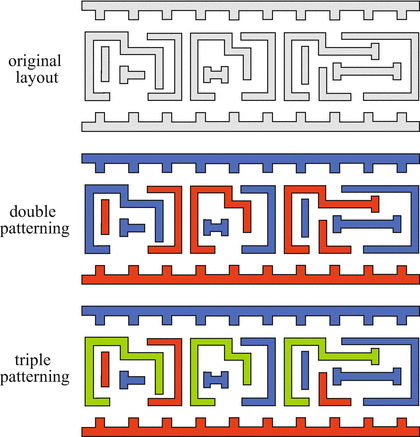
Decomposition of an original layout into two or three individual masks (Image: David Abercrombie; Mentor Graphics Corp.)
This type of pattern decomposition was used for process nodes between 22 nm and 14 nm. Actually, LELE lithography has never become very popular. It causes severe problems with overlay and requires doubling of the number of masks and exposures, or more in case of multi-patterning.
-
Use of self-aligned double patterning (SADP) (spacer lithography) .
In this technology the final pattern on the wafer is created by the formation of sub-resolution features during semiconductor process steps, rather than by sub-resolution lithography. The process flow in this technology is as follows (Fig. 3.24). The print target is shown in (a). As a first step, a hard mask layer is deposited or grown on the wafer. To support the formation of sub-resolution spacers a sacrificial polysilicon layer is deposited on the wafer and patterned with a relatively large optical lithography pitch (b). Since many of the layers are deposited with an atomic layer deposition (ALD) step, where no high temperature step is involved, the polysilicon is often replaced by photo-resist material. Next, an oxide (or nitride or other) layer is deposited on top of the structure and then etched back until sub-resolution sidewall spacers are left (c). Then the sacrificial polysilicon is removed (etched) (d), followed by a pattern transfer from spacer to hard mask (e). Finally the pattern in the hard mask is used to create the final pattern on the wafer (f). This spacer technology is a convenient approach to achieve sub-resolution patterning with relatively large optical resolution pitches, avoiding problems of e.g., overlay between successive exposures in a double patterning technology. Another advantage of this technique is that the printed critical dimension uniformity (CDU) is independent of the line-edge roughness (LER) . LER is caused by the diffusion of resist during a heat step after the exposure (post-exposure bake at 200–220 ∘C), but before the development of the resist. This diffusion is random and may lead to diffusion lengths of 40 nm, which causes intra-line variations leading to frayed lines. In spacer technology, however, the pattern transfer is done through spacers and not through resists, showing almost no LER. A disadvantage of the spacer lithography is that it is only applicable for mono CD (critical dimension) which reflects the smallest geometrical features (contacts, metal width,trenches, etc.), so, for patterns with only one width. Patterns with features that also have two times the line width can be produced by the formation of two spacers directly positioned next to each other. SADP [13] is preferably used in the creation of dense regular patterns of parallel fixed-pitched lines in only one direction. In litho-friendly designs, including FinFET designs, that contain fixed-pitched transistor gates, SADP is used for patterning the polysilicon layer (Fig. 3.25). In this case a pattern of continuous poly lines at a single pitch is printed first. Then, to create individual gates, the unwanted portions of the polysilicon are etched away by using a cut mask . This leads to a much improved CD-control and reproducibility of the polysilicon gates, because the final pattern is much less influenced by lithographic aberrations.
Fig. 3.24 
Basic steps in spacer lithography
Fig. 3.25 
Example of the use of the cut mask to create a much improved poly-CD control
The cut mask may contain a dense pattern of high resolution features, which will make it costly. SADP requires restricted design rules, resulting in patterning one-dimensional lines with fixed spacings. Patterning the critical metal layers in the back-end of the process demands a shift in IC design and requires 1-D metal patterns. The metal features in one metal layer are then fully orthogonal with respect to ones in the previous layer.
The SADP spacer lithography allows the pitch to be halved with just one single lithographic exposure step. The CD control is then determined by the thickness of the deposited spacer layer, which is very accurately controlled since the formation of this spacer layer is done with an atomic layer deposition step (ALD) . Let us assume that we now use the pattern structure in step e in Fig. 3.24 as a starting point for a second SADP iteration and we repeat steps c to f, then we have again doubled the number of features. This is often referred to as self-aligned quadruple patterning (SAQP) (Fig. 3.26). SADP double patterning is often used in advanced memories, because memories typically consist of uniform pattern distributions. Currently (2016) spacer lithography is also increasingly used in the formation of the fins in FinFET process nodes of 20 nm and beyond. Even logic circuits in advanced FinFET processes are increasingly built from fully regular layout patterns in the creation of fins and transistor gates. Section 4.8 in the next chapter describes a potential FinFET layout architecture in an example 16 nm CMOS process node.
Fig. 3.26 
Example of quadruple patterning using two iterations of self-aligned double patterning
-
Computational lithography . In Sect. 3.3.1 several resolution enhancement techniques (RETs), such as optical proximity correction (OPC), phase-shift mask (PSM) and off-axis illumination (OAI), have been discussed. OPC already uses a lot of computational effort to compensate lithographic aberrations by changing the patterns on the reticle. Computational lithography uses complex model-based mathematical algorithms to optimise these RETs. It models and simulates the light, from source to wafer as it travels through the reticle, the lenses and the photoresist. Potential light distortions are pre-corrected by changing the patterns on the reticle. It not only includes the adjustment of OPC geometries, but also accounts for variations in exposure time, dose and focus. The growth in the number of mask features combined with the increasing number of RETs has caused an exponential growth in computer simulation time. Many CPU years are required for the complete computational mask fabrication of a state-of-the-art chip. Mask-making companies run several graphic cards and other dedicated hardware accelerators in parallel to timely produce a complete chip mask set. Computational lithography, in combination with double or triple patterning, will enable the printing of 22 nm half pitch layouts.


3.3.3 Next Generation Lithography
-
Use of Extreme-UV (EUV) lithography . With a light source wave length of 13.5 nm, EUV is often regarded as the most probable potential lithography solution for technology nodes beyond 30 nm. However, EUV ‘light’ is absorbed by all materials, including air. Therefore mirrors have to be used in a vacuum-based system with reflective instead of refractive optics and reticles. Still a lot of problems need to be solved before it can be used in high-volume production. A few of them will be mentioned here. First, there is no suitable resist for high-volume production available, yet. Second, the light transmission takes place via a large number of mirror lenses (Fig. 3.27).
Fig. 3.27 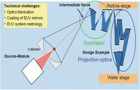
The transmission path of the light in an EUV scanner as it travels from source to wafer (Courtesy of: Carl Zeiss)
A laser-produced-plasma (LPP) source is used to deliver the required EUV power [17], by focussing a CO2 laser beam onto tiny tin (Sn) drops, each about 20 μm in diameter, creating highly ionised plasmas. These ions cause an isotropically radiation of EUV photons, which are gathered by a special coated ( ≈ 0.5 m) mirror called collector (Fig. 3.27) and focussed to an intermediate focus point , from where they are directed through the illuminator path, the reticle and the projection optics to the wafer. This puts stringent requirements on the EUV light source.
For high-volume production, with >100 wph scanner throughput assuming photoresist sensitivities at levels of 15 mJ/cm2 [19], EUV scanners require clean EUV power of 250 W at the intermediate focus point (IF point) to generate about 1 W EUV power at wafer level. This requires a laser output power of about 25 kW. With a laser efficiency of only 2.8%, this requires a total laser input electrical power of 0.88 MW [20], with instantaneous laser peak power of several MW [21].
It has been a struggle for almost a decade to combine the best EUV power source with the perfect resist to enable sufficient EUV power at wafer level. It should lead to acceptable throughput times, up to one hundred or more wafer exposures an hour. This explains the need for an improved light-transmission system to improve the throughput time and reduce the power consumption.
In 2006 the first EUV lithography tools (demo tool: US$ 65 million!!) have already been shipped. It was not meant for production but it will support R&D programs at IMEC (Leuven, Belgium) and at CNSE (University of Albany, New York) [18]. Pilot line production took off in 2012, when Intel, TSMC and Samsung start participation in a Co-Investment Program to enable acceleration of the development of key lithography technologies, particularly that of EUV. Although current immersion scanners show throughputs of 175–275 wafers per hour, the effective throughput with double, triple or quadruple patterning reduces with a factor of two, three or four, respectively. Currently (2016) EUV wafer throughput is close to 1000 wafers per day, based on 80 W IF power, with expected increase to 1500 wafers per day by the end of the year. With 250 W IF power and 15 mJ/cm2 resist sensitivity this number could increase to around 100 wafers per hour, which would make EUV [24] very competitive with alternative multi-patterning lithography technologies.
What is really important in the operating efficiency of an EUV lithography system is its average throughput. This is a combination of its actual throughput and its availability (uptime). Today’s availability is between 55 and 70%. ASML continuously rolls out new upgrades to increase uptime of their EUV systems. All leading semiconductor foundries plan to install EUV tools in their fabs, particularly for the 7 nm and 5 nm nodes, as soon as the average throughput of EUV systems is high enough (close to 100 wafers per hour) and turns out to be stable. The EUV is then expected to be used only for the most critical layers, while the other layers will still be printed with a combination of multi patterning and 193 nm immersion scanners.
Use of alternative techniques to fabricate image-critical patterns in sub-10 nm technologies. For many years, X-ray lithography (XRL) has been a potential candidate for next-generation lithography (NGL) . It uses X-rays, which generate photons with a wavelength often between 1 and 4 nm to expose the resist film deposited on the wafer, enabling much finer features than current optical lithography tools. However, it has some major disadvantages. Generally, at smaller wavelengths, all optical materials become opaque, but at X-ray wavelengths, these materials become transparent again. Moreover, at these wavelengths, the refraction index is almost 1.0 for all materials. Conventional lenses are unable to focus X-rays and, consequently, XRL tools cannot use a lens to shrink a mask’s features. Therefore its 1:1 pattern transfer methodology requires mask patterns with only one-fourth of the feature sizes used in the 4:1 photo-lithography masks. In addition, it requires an extremely expensive synchrotron, which converts an electron beam into an X-ray beam. It is therefore expected that the use of XRL will be limited to fabrication processes that create niche devices, such as MEMS.
-
An alternative to photolithography is the nano-imprint lithography (NIL) . This 1:1 technology is based on physically pressing a hard mold (typically identical to the quartz/chrome material commonly used for optical lithography) with a pattern of nano structures onto a thin blanket of thermal plastic monomer or polymer resist layer on the sample substrate, to which the structure needs to be replicated. This imprinting step is usually done with the resist heated, such that it becomes liquid and can be deformed by the pattern on the mold. After cooling down, the mold is separated from the sample, which now contains a copy of the original pattern. Its mayor advantage is that it can replicate features with nanometer dimensions [25]. This process is already used in volume production in electrical, optical and biological applications. For semiconductor applications, the ‘step-and-flash’ imprint (SFIL) seems to be the most viable one. It allows imprinting at room temperature with only a little pressure using a low-viscosity UV curing solution instead of the resist layer. The higher the sensitivity to UV, the less exposure time the solution needs and the higher the throughput. In this imprint technology some of the wafer process complexity has moved to the fabrication of the mold. Still a lot of key issues, particularly related to overlay and defects, need to be solved, but the results of this disruptive technology, so far, are promising. A potential barrier for using the imprint lithography is that it requires very advanced lithographic processes to create the patterns on the mold. Because it is a 1:1 pattern transfer process, the pattern dimensions are only one-fourth of those printed on a photo mask, which is one of its major challenges. Moreover, low throughput has become the real show stopper for this technology. Reference [25] discusses the process and potentials of nano-imprint in more detail. Recently, NIL is also seen as an alternative to photolithography in photonics applications, such as in the fabrication of LEDs and photovoltaic (PV) cells. For the fabrication of ICs, NIL has regained interest by a 3-D NAND flash manufacturer, as to reduce the production cost of NAND flash memories [22]. Line widths down to 15 nm are claimed, while the cost could be less than the use of quad-patterning techniques or EUV. The mold can be made using e-beam lithography.
-
E-beam lithography (EBL) is another alternative to photolithography. For a long time, the most important use of EBL is in the production of photomasks. Today it is also used as a direct-write lithography in the chip fabrication process. It uses a focused electron beam that directly writes the pattern shapes into the electron-sensitive resist layer on the wafer. The intensity of the electron beam changes the solubility properties of the resist material. Exposed areas, or their inverse, depending on the tone (positive or negative) of the resist, are then removed during a development step. Advanced SoC ICs may contain several billion transistors, connected by wires in about ten different metal layers and patterned by 35–40 masks. When all rectangles in each of the masks need to be written by a single e-beam, the throughput time of the total manufacturing process would explode. A solution to this problem is to use many e-beams in parallel. An example of such a mask-less lithography tool is based on a massively parallel electron-beam writing system that uses high speed optical data transport for switching the electron beams [23]. With 13,260 electron beams in parallel, this tool enables a throughput of 10 wph. The amount of data for each 26 × 33 mm field is 8 TB. One such tool has a footprint of 1. 1 × 1. 65 m. Due to its relatively low throughput, e-beam lithography applications are limited to prototype ICs and low-volume specialty products. Also in environments which explore semiconductor (test) circuits and designs, this mask-less lithography would avoid the development of an expensive mask set.


Moore’s law is driven by the economical requirements of the semiconductor markets. This means that all semiconductor disciplines (design, litho, diffusion, packaging, testing, etc.) are cost driven. For the lithography it means that there is a constant drive to make masks cheaper or to use cheaper masks for certain low-resolution process steps. Binary masks are relatively simple and cheap, but guarantee high throughput and can be non-destructively cleaned. Attenuated PSM masks suffer from radiation damage. Moreover, they are immersed in a chemical liquid for cleaning, which is a destructive process, such that they can only be cleaned a limited number of times and are therefore much more expensive. Today, radiation damage is reduced by roughly 40% by using so-called AID (Anti-Irradiation Damage) PSM. It also improves cleaning durability.
To minimise mask costs during the fabrication process, the more expensive masks are only used to image those patterns that really need the smallest feature sizes. For the production of one type of memory for example, different mask categories can be used. To reduce the production costs of a flash memory process of 22 masks, it may use 4 ArF (attPSM + OPC) masks, 12 KrF (6 binary and 6 attPSM) and 6 I-line (binary) masks.
Finally, particularly the semiconductor memory vendors have found a way to increase bit density without the use of very advanced and expensive lithography tools. By using multiple layers of silicon (3D stacked silicon) , memory capacity can be increased dramatically, without increasing the footprint of the memory chip. Some SRAM products use cells with three vertically stacked transistors, while some flash memories are currently being fabricated using tens of stacked layers of memory cells. The first OTPs built from four memory cell layers were already introduced in 2004. NAND flashes with 48 layers of silicon are in development. 3-D technologies are only economically viable when the complexity of the devices fabricated in these stacked layers is very limited. Because non-volatile memories use only one type of transistor in the cells (see Chap. 6) they are particularly suited for 3-D stacking. Therefore these layers are only used to fabricate arrays of memory cells and require only a very limited number (zero (3-D NAND flash) to three) masks per layer, which can be fabricated by existing photolithography tools. These arrays use the peripheral address selection and sense amplifier circuits of the original first memory array located at wafer level.
3.3.4 Mask Cost Reduction Techniques for Low-Volume Production
The amount to which mask cost contribute to the total chip development cost depends on the application area (volume) of the chip. This has a direct relation with the number of wafer exposures per mask, which varies from 500 for ASICs, 5000 for microprocessors (e.g., Intel, AMD, etc.) to more than 10,000 for stand-alone memories. As such, the mask cost per chip for high volume DRAMs and NAND flash memories are neglectable, while they can be more than 10% in low-volume applications as medical and aviation. The cost of a mask set increases with shrinking process nodes. In fact, it doubles when compared at their year of introduction [26]. It then reduces roughly with an average of 20% per year. A mask set for 32 nm could cost close to three million US$. Close to two thirds of the masks are non-critical, in that they can be implemented as simple binary masks. The other third can be considered as critical, of which two or three masks fall in the category of extremely critical [3]. The critical masks can be produced with scanning-laser equipment with rather good throughput, while e-beam equipment is required for the extremely critical masks which may require 24 h of e-beam exposure time. For comparison, when a typical binary mask using aggressive OPC may cost $20k, then a moderate phase-shift halftone mask will cost $50k, while a real hard phase shift mask will cost about $130k. With the introduction of double, triple and quadruple patterning or EUV lithography the mask cost will even further increase. There are several approaches to reduce mask cost.
On so-called multi-project wafers (MPW) several products are included on the same mask set to reduce overall mask costs (Fig. 3.28).


Example of a multi-project wafer (MPW)
Another way to share the mask costs is the multi-layer reticle (MLR) , on which several mask layers of the same product are grouped together to reduce the physical number of masks. These MLRs do not combine designs of different products. Both techniques are particularly used for small-volume designs, for prototyping, and for educational purposes. To save mask costs completely, direct-writing techniques use an electron-beam (e-beam) or laser-beam system, which writes the layout pattern directly onto a wafer resist layer, without using a mask. It requires the deposition of an additional conductive layer on the resist layer, to prevent damage by electron charging during the patterning process. The resolution yielded by an e-beam machine is better than 5 nm, but at a lower throughput, because it writes every feature individually. It is free of wavelength aberration. Laser-beam systems are gaining market share at the cost of e-beam systems, because they are cheaper since they do not require a vacuum environment. Because of their low throughput, both e-beam and laser-beam systems usage, today, is limited to fabricate low-volume samples, such as MPWs, prototyping products and test silicon for process development. Next to that these techniques are used to fabricate the physical glass-chrome masks (reticles) for use in photolithography processes. These direct-writing techniques are also called mask-less lithography (MLL or ML2) and are currently also being explored as an alternative for, or successor of the conventional photolithography, even for high volume production. The main reason is the rapidly increasing costs of an optical mask set, which reaches the $2 million mark for the 65 nm node, although these costs will reduce when the process is getting more mature. Over the last decade, a lot of progress has already been made to improve throughput. The potentials of mask-less e-beam lithography are further discussed in [27].
More information on future lithography techniques can be found in numerous publications and also on the internet and is beyond the scope of this book. To summarise the evolution of the wafer stepper/scanner, Table 3.2 presents several key parameters which reflect the improvements made over different generations of steppers/scanners.
3.3.5 Pattern Imaging
The photolithographic steps involved in the transfer of a mask pattern to a wafer are explained with the aid of Fig. 3.29. Usually, the first step is oxidation and comprises the growth of a 30–50 nm thick silicon-dioxide (SiO2) layer on the wafer. Subsequently, a nitride (Si3N4) layer is deposited (Fig. 3.29a). Next, this nitride layer is covered with a 0.5–2 μm thick photoresist layer (Fig. 3.29b). The mask is used to selectively expose the photoresist layer to light (Fig. 3.29c, d). This exposure causes a change in the chemical properties of the resist, so that it can be removed by a special solution (developer). The photoresist is then developed, which leads to the removal of the exposed areas if the photoresist is positive . The resulting pattern in the resist after development (Fig. 3.29e) acts as an etch barrier in the subsequent nitride etching step (Fig. 3.29f), in which the unprotected nitride is removed (stripped). Finally, the remaining resist is removed and an image of the mask pattern remains in the nitride layer (Fig. 3.29g). This nitride pattern acts as a barrier for a subsequent processing step.


Pattern transfer from mask to wafer
Both positive and negative resists exist. The differences in physical properties of these resist materials result in inverting images, see Fig. 3.30.


The use of positive and negative resist for pattern imaging
The combination of pattern transfer and one or more processing steps is repeated for all masks required to manufacture the IC. The types of layers used for the pattern transfer may differ from the silicon-dioxide and silicon-nitride layers described above.
The principle, however, remains the same. The processing steps that follow pattern transfer may comprise etching, oxidation, implantation or diffusion and planarisation. Deposition is also an important processing step. These steps are described in detail in the following sections.
3.4 Oxidation
The dielectrics used in the manufacture of nanometer CMOS circuits must fulfil several important requirements [30]:
-
high breakdown voltage
-
low dielectric constant of inter metal dielectrics
-
high dielectric constant for gate dielectric
-
no built-in charge
-
good adhesion to other process materials
-
low defect density (no pinholes)
-
easy to be etched
-
permeable to hydrogen.
One of the materials that incorporates most of these properties is silicon dioxide (SiO2). SiO2 can be created by different processes: thermal oxidation or deposition. A thermal oxide was used to isolate the transistor areas in conventional MOS ICs. In these isolation areas, the oxide must be relatively thick to allow low capacitive values for signals (tracks) which cross these areas. This thick oxide was created by exposing the monocrystalline silicon substrate to pure oxygen or water vapour at a high temperature of 900–1200 ∘C. The oxygen and water vapour molecules can easily diffuse through the resulting silicon dioxide at these temperatures. The following respective chemical reactions occur when the oxygen and water vapour reach the silicon surface:
The Local Oxidation of Silicon (LOCOS) process is an oxidation technique which has found universal acceptance in MOS processes with gate lengths down to 0. 5 μm. Silicon is substantially consumed at the wafer surface during this process. The resulting silicon-dioxide layer extends about 46% below the original wafer surface and about 54% above it. The exact percentages are determined by the concentration of the oxide, which contains about 2. 3 ⋅ 1022 atoms/cm3, while silicon contains about 5 ⋅ 1022 atoms/cm3. A disadvantage of the LOCOS process is the associated rounded thick oxide edge. This bird’s beak is shown in Fig. 3.31a.


Comparison of (a ) a conventional LOCOS process and (b ) use of shallow-trench isolation (STI) to isolate transistors
The formation of the bird’s beak causes a loss of geometric control, which becomes considerable as transistor sizes shrink. Intensive research efforts aimed at suppression of bird’s beak formation have resulted in lengths of just 0.1–0.15 μm for an oxide thickness of 0. 5 μm. Even with a suppressed bird’s beak, the use of LOCOS is limited to the isolation of over-0. 25 μm process nodes.
An important alternative to these LOCOS techniques, already used in 0. 35 μm CMOS technologies and below, is the Shallow-Trench Isolation (STI) . STI uses deposited dielectrics to fill trenches which are etched in the silicon between active areas. The use of STI for nanometer technologies is discussed later in this chapter (Sect. 3.9.3).
Another important application of thermally grown oxide was the oxide layer between a transistor gate and the substrate in conventional CMOS processes. This ‘gate oxide’ must be of high quality and very reliable. Defects such as pinholes and oxide charges have a negative effect on electrical performance and transistor lifetime . Because the gate oxide is only a few atoms thick, it is particularly a challenge for the industry to scale it further and/or find alternative ways to increase its capacitance. Figure 3.32 shows a cross section of a MOS transistor.


Schematic cross section of a MOS transistor
The gate-oxide thickness must be sufficiently uniform across the die, from die to die, from wafer to wafer, and from run to run. It scales with the technology node according to Table 3.3, which shows representative values for various technology nodes. L represents the physical gate length.
The table also shows the divergence in gate oxide thicknesses, supply and threshold voltages. This is due to the fact that today’s semiconductor technologies must support applications with a wide range of performance requirements: high-density, low active power, low standby power, high speed, etc. In each technology node, the input- and output (I/O) transistors usually operate at a larger voltage (1.2 V, 1.8 V, 2.5 V and/or 3.3 V) and require an additional oxide thickness and threshold voltage. The simultaneous use of more oxide thicknesses and threshold voltages in one process is of course at the cost of more mask, lithography and processing steps. Each of the processes offers usually only two or three different threshold voltages, to limit the number of masks, lithography and processing steps. Technology nodes, today, offer different process versions, e.g., a high-performance (HP) , a low-operating power (LOP) and a low-standby power (LSTP) process . Characteristics for these processes are shown in Table 3.4, according to the ITRS roadmap [31].
Although most of these processes include high-ε/metal gates, the oxide thickness (t ox) is still expressed as if silicon-dioxide was used for the gate dielectric. Therefore, the equivalent oxide thickness (EOT) refers to an equivalent silicon-dioxide thickness with the same capacitance value as the used high-ε dielectric stack.
The use of dielectric SiO2 layers below about 2 nm thickness causes gate oxide direct tunnelling , resulting in currents which may exceed a level of 1 A/cm2. At these gate-oxide thicknesses, pMOS transistors with heavily boron-doped polysilicon suffer from boron penetration into the gate oxide, causing an undesirable positive threshold-voltage shift and a performance and reliability degradation. The quality of the gate oxide is greatly improved with nitrided gate oxide (SiON) [32], wherein a conventionally created silicon oxide dielectric is impregnated with a small dose of nitrogen. It reduces boron penetration and improves gate oxide breakdown characteristics and reliability [34]. It also leads to a minor increase in the dielectric constant. On the other hand, too much nitrogen close to the gate-oxide/Si-substrate interface enhances Negative Bias Temperature Instability (NBTI; see also Chap. 9) [35]. Moreover, the combination of thinner gate oxide and increased channel doping also causes depletion of the bottom region of the gate material and this effect becomes more pronounced with further scaling of the oxide thickness. This is called gate depletion . As a result of these effects, the double-flavoured polysilicon (n+ doped gate for nMOS transistors and p+ doped gate for pMOS transistors) is replaced by a metal. Other alternatives, which were under research and also prevent gate depletion, include fully silicided (FUSI) polysilicon gates. Section 3.9.4 discusses further details on FUSI gates and high-ε/metal gate processes. Most advanced CMOS processes use atomic-layer deposition (ALD) to fabricate the very thin gate-oxide layer. This is discussed in the next subsection.
3.5 Deposition
The deposition of thin layers of dielectrical material, polysilicon and metal is an important aspect of IC production.
The growth of an epitaxial film (layer) is the result of a deposition step combined with a chemical reaction between the deposited and substrate material. The term epitaxy is based on the Greek words epi, which means ‘above’, and taxis, which means ‘in ordered manner’. Therefore epitaxial can be translated as ‘in an ordered manner arranged upon’. If the deposited layer is the same material as the substrate, it is called homo-epitaxy or epi-layer for short. Silicon on sapphire is an example of hetero-epitaxy , in which the deposited and substrate materials differ [36]. Epitaxial deposition is created by a Chemical Vapour Deposition (CVD) process. This is a process during which vapour-phase reactants are transported to and react with the substrate surface, thereby creating a film and some by-products. These by-products are then removed from the surface. Normally, the actual film created by a CVD process is the result of a sequence of chemical reactions. However, a different overall reaction can generally be given for each of the silicon sources. The hydrogen reduction of silicon tetrachloride (SiCl4), for example, can be represented as:
Several parameters determine the growth rate of a film, including the source material and deposition temperature. Usually, high temperatures ( > 1000 ∘C) are used for the depositions because the growth rate is then less dependent on the temperature and thus shows fewer thickness variations. The overall reaction for the deposition of polysilicon is:
This reaction can take place at lower temperatures, because SiH4 decomposes at a higher rate. The creation of dielectric layers during IC manufacture is also performed by some form of CVD process. The most commonly used dielectric materials are silicon dioxide (SiO2) and silicon nitride (Si3N4). In an Atmospheric-Pressure CVD (APCVD) process, the material is deposited by gas-phase reactions. This deposition generally results in overhangs and a poor step coverage (Fig. 3.34). APCVD is currently used to deposit Boron PhosphoSilicate Glass (BPSG) epitaxial layers and form the scratch-protection layer or passivation layer (PSG). PSG is a phosphorus-doped silicon dioxide dielectric which is deposited on top of polysilicon (between polysilicon and first metal) to create a smooth topography that is beneficial for the deposition of the metal layers. BPSG contains boron and phosphorus for a better flow (spread) of the dielectric. The phosphorus also serves to improve internal passivation. The following reactions apply for the deposition of SiO2 and Si3N4, respectively:
Two versions of CVD have been introduced by the above reactions: LPCVD and PECVD. LPCVD is a low-pressure CVD process, usually performed in a vacuum chamber at medium vacuum (0.25–2.0 torr) and at temperatures between 550 and 750 ∘C. Under these conditions, the vapour-phase reactions are suppressed, while the decomposition now occurs at the surface, leading to a much better step coverage. In the previously discussed CVD process, the chemical reactions are initiated and sustained only by thermal energy. PECVD is a plasma-enhanced CVD process. A plasma is defined to be a partially ionised gas which contains charged particles (ions and electrons) and neutrals. The plasma is generated by applying an RF field to a low-pressure gas, thereby creating free electrons within the discharge regions [36]. The electrons gain sufficient energy so that they collide with gas molecules, thereby causing gas-phase dissociation and ionisation of the reactant gases. At room temperature, a plasma therefore already contains high-energy electrons. Thus, even at low temperatures, a PECVD process can generate reactive particles; it therefore has a higher deposition rate than other CVD processes.
If we compare the previous reactions to depositing SiO2, we see that the LPCVD which occurs at high temperature therefore needs no additional oxygen, while the PECVD process needs additional oxygen because the oxygen cannot be dissociated from the TEOS (tetra ethylorthosilicate: Si(OC2H5)4) at low temperatures. A Sub-Atmospheric CVD (SACVD) process occurs at temperatures around 700–800 ∘C. Because of the high pressure ( ≈ 1/2 atmosphere instead of a few torr), the deposition speed will be higher, resulting in a higher throughput. This form of CVD is particularly used for BPSG.
Metal layers are deposited by both physical and chemical methods. In Physical Vapour Deposition (PVD) methods, such as evaporation and sputtering, the material is physically moved onto the substrate. PVD-evaporation is a deposition process, in which a vapour of the material to be deposited is transported to the wafer in a low-pressure environment. After condensation at the wafer surface, it forms a thin film on it. When using the PVD-sputtering technique for the deposition of aluminium, for instance, an aluminium target is bombarded with argon ions, which physically dislodge aluminium molecules from the target, causing a flux of aluminium to flow from the target to the wafer surface. The aluminium was alloyed with 0.5% copper to improve elctromigration behaviour. After deposition of the aluminium photolithographic and etching steps are used to create the required metal pattern.
Copper cannot be deposited and etched as easy as aluminium. Potential etching plasmas create non-volatile residuals that remain on the wafer. Moreover, copper diffuses through oxides leading to transistor threshold voltage shifts and reliability problems. Therefore, a copper back-end technology is quite different from a conventional aluminium one. In the latter, the aluminium deposition step is followed by a dry etching step to etch the metal away according to the mask pattern and then filling the gaps with a dielectric. A copper back-end uses a so-called damascene process flow , in which the conventional subtractive metal etching process flow is replaced by a metal inlay process flow. Figure 3.33 shows a comparison of both flows.


Comparison of conventional and damascene processing
In a damascene process, first an oxide layer is deposited, identical to an aluminium back-end process. Then an etch-stop layer is deposited on top of this oxide layer, followed by the deposition of another oxide layer. These oxide layers are also referred to as inter-level dielectric (ILD) layers. Next, an oxide etching step creates trenches in the top oxide layer, according to the pattern in the corresponding metal mask. The etch-stop barrier blocks the etching process, such that it cannot etch the lower oxide layer. Then a thin barrier layer is deposited by an atomic layer deposition (ALD) step on top of the ILD layer and prevents the diffusion of copper. This layer is a combination of Ta and TaN. In fact the deposition starts with a Ta of a few atomic layers thick and then gradually increase the amount of N such that the last atomic layers consist of TaN. Next, a seed layer is deposited to provide a conductive layer, which is required for the electroplate-deposition process of the copper, to improve copper adhesion and coverage. Then, copper deposition is done, using an electro-chemical process: electroplating, in which the wafer is immersed in a (salt/acid) solution of copper sulfate (and some other acids and/or additives to enhance the filling capabilities) and connected to a negative terminal of the power supply. The positive supply terminal is connected to a copper body, which creates copper ions into the salt solution. These positively charged copper ions are attracted to the negative wafer surface and form a thick copper blanket across the total wafer. Then a planarisation step, called CMP (Sect. 3.8) polishes the wafer until it has reached the bottom of the barrier layer (copper and barrier are removed in one step!). Copper tracks are then remaining as a metal inlay in the trenches (Damascene processing), similar to the metal inlay in swords, made in ancient times in Damascus, Syria. Then again a barrier layer is deposited to cover the top of the copper inlays, such that copper is fully encapsulated within the barrier layer. In 20 nm CMOS process the barrier may consist of a TaN film and a Ta film, each of which is deposited with ALD technology with a thickness of approximately 3 nm each. Because the copper width in this node and smaller nodes will be so narrow, the chance of creating voids (poor copper fill) is rapidly increasing. By depositing a thin cobalt film before the copper deposition greatly improves the copper’s fill performance at smaller geometries, leading to less voids and improved electromigration properties [37]. After the copper layer has been deposited on the cobalt barrier layer and planarised thereafter, the top barrier layer is then formed by a selective cobalt deposition only on the copper tracks. This is done by exposing the substrate to a cobalt precursor gas to selectively form a cobalt capping layer over the copper surface while leaving exposed the dielectric surface during a vapour deposition process [38].
Today, most fabs use a dual-damascene backend, in which both the vias (also called studs, or pillars, which are contacts between two metal layers) and trenches are simultaneously etched into the ILD layer. Also in the next sequence of deposition steps for the barrier, the seed layer and the electroplate copper, respectively, the vias and tracks are simultaneously filled, thereby reducing processing costs.
Although the resistance of copper is 40% less than that of aluminium, this advantage cannot fully be exploited, because part of the available track volume is occupied by the barrier material, which has a much higher resistance value. The use of copper instead of aluminium for interconnection resulted in only a limited reduction of the effective interconnect resistivity by 25–30%. In combination with the use of low-ε dielectrics, the interconnect capacitance is reduced and leads to faster or less-power circuits. Copper can also withstand higher current densities, resulting in a reduced chance of electromigration (see Chap. 9).
CVD methods form the chemical alternative for the deposition of metals. Tungsten (W), for example, may yield the following CVD reaction:
The choice of deposition method is determined by a number of factors, of which step coverage is the most important. Figure 3.34 shows an example of bad aluminium step coverage on a contact hole in a conventional CMOS process. Such a step coverage can dramatically reduce the lifetime of an IC . It also causes problems during further processing steps and the associated temperature variations can lead to voids in the aluminium.


Example of poor step coverage in a conventional CMOS process
Moreover, the local narrowings cannot withstand high current densities. Current densities of ≈ 105 A∕cm2 are not exceptional in modern integrated circuits. Excessive current densities in metal tracks cause electromigration . This leads to the physical destruction of metal tracks and is another phenomenon that reduces the reliability of ICs. This topic is examined more closely in Chap. 9.
One deposition step that got a lot of attention over the last decade and which was already mentioned before is the so-called atomic layer deposition (ALD), particularly for its potential applications in advanced (high-ε) gate dielectrics, DRAM capacitor dielectrics and copper diffusion barriers in advanced CMOS and memory processes. Without going deep into the chemical and physical reactions, ALD basically uses pulses of gas, creating one atomic layer at a time. So, the deposited film thickness is only dependent on the number of deposition cycles providing extremely high uniformity and thickness control. It is therefore also of interest in all (sub) nanometer applications that benefit from accurate control of (ultra-) thin films. The drive for ALD development was to replace the thermally grown thin gate oxide layer creation. ALD is a cyclic process with a low thermal budget. The film deposition consists of a repetition of these cycles, with every single cycle creating a one-atomic-thick layer film. More details on ALD can be found in [33, 39].
3.6 Etching
Many of the deposited layers require an etching step to remove the material where it is not needed. For example, to create a polysilcon gate pattern, first the whole wafer is deposited with polysilicon and next, it is etched away according to the polysicilon mask pattern, at locations where no polysilicon tracks are needed. The photolithographic steps described in Sect. 3.3.5 produce a pattern in a nitride or equivalent barrier layer. This pattern acts as a protection while its image is duplicated on its underlying layer by means of etching processes. There are several different etching techniques. The etching process must fulfil the following requirements: a high degree of anisotropy, good dimensional control, a high etching rate to minimise processing time, a high selectivity for different materials, a perfect homogeneity and reproducibility (e.g., eight billion trenches in a 8 Gb DRAM) and a limited damage or contamination to satisfy reliability standards. The degree of anisotropy depends on the requirements of the process step, e.g., during the STI etch an extremely vertical and sharp profile may increase stress and the occurrence of defects.
With wet etching , the wafer is immersed in a chemical etching liquid. The wet-etching methods are isotropic , i.e., the etching rate is the same in all directions. The associated ‘under-etch’ problem illustrated in Fig. 3.35a becomes serious when the minimum line width of the etched layer approaches its thickness.


The results of different etching methods. (a ) Isotropic. (b ) Anisotropic
Dry etching methods may consist of both physical and chemical processes (anisotropic) or of a chemical process only (isotropic). Dry-etching methods, which use a plasma, allow anisotropic etching, i.e., the etching process is limited to one direction by the perpendicular trajectory of the ions used at the wafer surface. The result, shown in Fig. 3.35b, is an accurate copy of the mask pattern on the underlying layer.
With plasma etching techniques [28], the wafers are immersed in a plasma containing chlorine or fluorine ions that etch, e.g., Al and SiO2 respectively. It comprises a plasma chamber, which contains a certain process gas. To transfer from the gas state into the plasma state, the chamber is pumped to the required pressure and energy is supplied to produce a glow-discharge plasma by a radio frequency (RF) electromagnetic field. This causes ionisation of the low-temperature plasma: after collision with molecules, they create many different gaseous species: free radicals, electrons, ions, neutrals, photons and by-products. These are then accelerated by an electrical field towards the surface material, which can then be etched quickly and selectively. The etching process depends on the gas pressure and flux and on the applied RF field. In sputter etching techniques , the wafer is bombarded by gas ions such as argon (Ar+). As a result, the atoms at the wafer surface are physically dislodged and removed.
Finally, a combination of plasma and sputter etching techniques is used in Reactive Ion Etching (RIE) . During RIE ionised gaseous molecules from the plasma are accelerated by an electric field toward the surface and react with the surface atoms forming new electrically neutral molecules which then floats away.
Satisfactory etching processes have been developed for most materials that are currently used in IC manufacturing processes. New process generations, however, require improved selectivity, uniformity, reproducibility and process control. Selectivity can be improved by the compound of the gaseous plasma or by the creation of polymers at the underlying layer. The use of an additional carbonaceous substance such as CHF3 during etching enhances its anisotropic properties. The use of this substance creates a thin layer close to the side wall of a contact hole, for example, which improves the anisotropy of the etching process. A second advantage is that carbon reacts with oxygen. It therefore increases the selectivity of the etching process because, when used in the etching of a contact-to-silicon, the reaction is stopped immediately on arrival at the silicon surface. Carbon does not react with silicon.
For critical anisotropic etching steps, both low-pressure etching techniques and High-Density Plasma (HDP) techniques are used. In HDP, energy is coupled into the plasma inductively to increase the number of free electrons. HDP is operated at low (some mtorr) pressure. This in turn results in a higher plasma density and a higher degree of ionisation. HDP is used to provide high-aspect ratios.
During the formation of the transistors also a combination of anisotropic (dry-etching) and isotropic etching (wet-etching) is used. Particularly in the formation of STI, the anisotropic etching step is used to create the steep edges of the trench, while an isotropic etching step is used at the end of the STI etching process, to create smooth very round corners in the bottom of these trenches. Rounded corners, both in the top and the bottom of the STI, limit the local electric field and reduce leakage currents. After etching the trenches, better rounded corners can be achieved by a high-temperature thermal oxidation, which reduces stress in the substrate. In the advanced 3-D memory architectures, such as DRAMs and NAND flash memories, many etching steps require high to extremely high aspect ratios of the contact holes. In the DRAM memories the third dimension is often used to stack various dies on top of each other and use through-silicon via (TSV) etching techniques to connect the individual dies. 3-D NAND-flash memories introduce some significant changes to the traditional etching techniques. In these devices, the 3rd dimension is used to produce many different layers of memory cells stacked on top of each other. The related extremely high aspect ratios for contacts (up to 100) require new etching techniques. Figure 3.36 shows a cross section of a 3-D example NAND-flash memory [29]. Details about these etching techniques are beyond the scope of this book. Further details on 3-D memories can be found in Chap. 6.


Cross section of the etching requirements in an example 3-D NAND flash (Courtesy of Applied Materials)
Complementary to atomic layer deposition to form extremely thin layers on a wafer, atomic layer etching (ALEt) enables the etching of layers with atomic precision [33]. ALEt is sometimes also called reverse ALD. ALEt has already been researched for more than two decades. The application area of ALEt is much less than that of ALD while the process is more complex. It still requires a lot of R&D effort, before it will become available in the high-volume production of semiconductor devices and ICs. The focus on new etching techniques does not preclude further development of existing techniques such as high-pressure etching and RIE.
Many process steps use plasma or sputter-etching techniques, in which charged particles are collected on conducting surface materials (polysilicon, metals). Also during ion implantation, charge can be built up. These techniques can create significant electrical fields across the thin gate oxides; this is called the antenna effect . The gate oxide can be stressed to such an extent that it can be damaged (so-called process or plasma-induced damage: PID) and the transistor’s reliability can no longer be guaranteed. The antenna effect can also cause a V T-shift, which affects matching of transistors in analog functions. It is industry practice to introduce additional ‘antenna design rules’ to limit the ratio of antenna area to gate oxide area. There are different rules for polysilicon, contact, via and metal-antenna ratios. These ratios may vary e.g., from 10 (contact-on-poly area to poly-gate area) to 5000 (accumulated-metal area to poly-gate area). An antenna rule, for example, may limit the maximum wire length in a certain metal layer to several hundred micron, depending on the metal layer and process technology. Also, in some libraries, protection diodes are used to shunt the gate. Each input to a logic gate in a standard-cell library then contains a protection diode.
3.7 Diffusion and Ion Implantation
Diffusion and ion implantation are the two most commonly used methods to force impurities or dopants into the silicon.
3.7.1 Diffusion
Diffusion is the process by which the impurities are spread as a result of the existing gradient in the concentration of the chemical. Diffusion is often a two-step process.
The first step is called pre-deposition and comprises the deposition of a high concentration of the required impurity. The impurities penetrate some tenths of a micrometer into the silicon, generally at temperatures between 700 and 900 ∘C. Assuming that the impurities flow in one direction, then the flux is expressed as:
where D represents the diffusion coefficient of the impurity in [cm2/s] and \(\frac{\delta C} {\delta x}\) is the impurity concentration gradient.
As the diffusion strongly depends on temperature, each different diffusion process requires individual calibration for different processing conditions. During the diffusion process, silicon atoms in the lattice are then substituted by impurity atoms.
The second step is called drive-in diffusion. This high-temperature ( > 1000 ∘C) step decreases the surface impurity concentration, forces the impurity deeper into the wafer, creates a better homogeneous distribution of the impurities and activates the dopants. This drive-in diffusion also causes an identical lateral diffusion.
As a result of the increased requirements of accurate doping and doping profiles, diffusion techniques are losing favour and ion implantation has become the most popular method for introducing impurities into silicon.
3.7.2 Ion Implantation
The ion implantation process is quite different from the diffusion process. It takes place in an ion implanter , which comprises a vacuum chamber and an ion source that can supply phosphorus, arsenic or boron ions, for example. The silicon wafers are placed in the vacuum chamber and the ions are accelerated towards the silicon under the influence of electric and magnetic fields. The penetration depth in the silicon depends on the ion energy. This is determined by the mass and electrical charge of the ion and the value of the accelerating voltage. Ion implanters are equipped with a mass spectrometer (analysing magnet), which ensures that only ions of the correct mass and charge can reach the silicon wafer. Ion implantation is characterised by the following four parameters:
-
The type of ion. Generally, this is phosphorus, arsenic or boron. The mass and electrical charge of the ion are important.
-
The accelerating voltage (V ), which varies from a few kilovolt to several MV.
-
The current strength (I), which usually lies between 0. 1 μA and 1 mA. High current implanters may use even higher currents.
-
The implantation duration (t), which is in the order of tens of seconds per wafer. The total charge Q = I ⋅ t determines the number of ions that will enter the silicon. Typical doses range from 1011 to 1018 atoms/cm2.
Variables V, I and t can be measured with very high accuracy. This makes ion implantation much more reproducible for doping silicon than classical diffusion techniques. In addition, V and I can be varied as a function of t to produce a large variety of doping profiles that are not possible with diffusion. The maximum impurity concentration is almost always at the surface when diffusion techniques are used.
The ion implantation technique, however, can be used to selectively create profiles with peaks below the wafer surface. The concentration of impurities decreases toward the wafer surface in these ‘retrograde profiles’ . The most important material that is used to mask ion implanting is photoresist. Ion implantation causes serious damage (disorder) in the crystal lattice of the target. In addition, only a fraction of the implanted ions occupies a silicon atom location. The other part does not occupy lattice sites. The interstitial dope atoms are electrically inactive and do not operate as donors or acceptors. A subsequent thermal (activation) step, at temperatures between 600 and 1100 ∘C, is used to recover the crystal structure. Another intention of this annealing process is to cause the vast majority of the dopants to become electrically active on the lattice sites. A disadvantage of this annealing step is that at a high temperature the doping atoms diffuse in all directions thereby increasing the junction depth and reducing the channel length. Rapid thermal anneal (RTA) is a short temperature cycle to limit the diffusion. It consists of a constant temperature (e.g. 600 ∘C) for stabilisation, followed by a temperature spike of just a few seconds. Then a radiative cooling step in the order of 30 s takes the temperature back to the normal value.
Because of the high energy involved, the equipment needs to be cooled and the focussed ion beam, which may have a beam size of around 20 cm2, must be scanned over the wafer to avoid heating. This scan follows a very controlled pattern, to create both a sufficiently high local and global dose uniformity. Ion implantation adds flexibility and increased process control to CMOS manufacture. It is superior to chemical deposition techniques for the control of impurities ranging from 1014 to 1021 atoms∕cm3. The heart of an ion implanter is formed by an ion source, usually an RF-activated plasma, from which ions are extracted by a small electric field, and a 90∘ analysing magnet. Because the ion beam is a mixture of different fractions of molecules and atoms of the source material, the 90∘ analysing magnet causes only the selected ions, with exactly the right charge and mass, that face equal centrifugal and centripetal forces, to reach the wafer through the accelerator column and the resolving aperture, see Fig. 3.37 and [40]. Lighter ions strike the inner wall; heavier ions strike the outer wall.


Schematic drawing of an ion implanter
Ion implantation is an essential and accurate technology to dope various regions inside, in between and below the transistors. Examples of the use of ion implantation are:
-
threshold voltage adjustment (e.g., 1 ⋅ 1018–5 ⋅ 1018 atoms/cm3, however this leads to a steep retrograde dope profile, in which the surface (channel) dope concentration is between 1 ⋅ 1017 and 5 ⋅ 1017 atoms/cm3; see Table 3.3 for the different threshold voltages that are currently applied in the different technology nodes.)
-
retrograde-well implantation
-
channel-stop implantation
-
source/drain formation (including S/D implants and S/D extension implants)
-
halo implant
-
triple-well implant
-
doping of 3-dimensional architectures used in memories (DRAM and flash)
Non-ideal aspects of ion implantation:
-
lateral distribution of impurities is not completely zero
-
throughput is lower than in diffusion process
-
complex and expensive implanters
-
initial cost of equipment: 2–5 M$.
The depth of the source and drain junctions are often in the same order of magnitude as the transistor channel length. The use of ion implantation in the formation of source/drain extension regions becomes increasingly challenging as these junctions become very shallow (4–20 nm) in advanced processes. Source/drain extension depths are in the order of 1/3 of the deep source/drain depths. The doping concentration does not change much with scaling. Only the energy during implantation must be adjusted to create those shallow junctions. Silicidation of sources and drains becomes a problem in that silicide can penetrate through the shallow junctions. This is called junction spiking . Unsilicided sources and drains show a five to ten times higher sheet and contact resistance, affecting the electrical properties of the transistors. Because of this, all modern CMOS processes today use silicided sources and drains. More on the creation of sources and drains in advanced CMOS processes can be found in Sect. 3.9.4. During the implantation process, the stationary ion beam is scanned over the wafers, which are positioned with 13 on a rotating disc. The wafer scan follows a controlled pattern to create sufficiently high local and global dose uniformities. The implant equipment must be cooled during use. The implant beam size may be in the order of 20 cm2. The formation of nMOS and pMOS transistors require a large number of different implants (see Fig. 3.46) for: the wells, the sources and drains, their extension and halo implants, their threshold implants (e.g. low-V t and high-V t), etc. Advanced wafer fabs, which produce one to several hundred thousand wafers per month, with processes that use 50 or more different implants, may therefore require 20 different implanters, each with a capacity of more than 200 wafers/hour.
The doping concentration with diffusion is always higher towards the surface of the wafer, with the peak dope at the surface. With ion implantation, we can accurately adjust the ion implant acceleration speed, thereby creating the peak dope at a very well controlled distance below the surface. Such an implant is also called a retrograde implant. Retrograde implant profiles are particularly used in the formation of the wells, as discussed in Section 3.9.3.
3.8 Planarisation
The increase in the number of processing steps, combined with a decrease in feature sizes, results in an increasingly uneven surface. For example: after completing the transistors, an isolation layer is deposited before the metal layers are deposited and patterned. The step height of the underlying surface is replicated into this isolation layer. This introduces two potential problems in the fabrication process. When the first metal is directly deposited onto this layer, its thickness can dramatically reduce at these steps, causing an increase in metal resistance and an increase in the occurrence of electromigration. Secondly, as already discussed in the lithography section, new lithography tools allow a smaller depth-of-focus (DOF), tolerating only very small height variations. During imaging, these variations can introduce focus problems at the high and low areas. Therefore, all current CMOS processes use several planarisation steps. These steps flatten or ‘planarise’ the surface before the next processing step is performed.
In conventional CMOS processes, planarisation was used during the back-end of the process, i.e., in between the formation of successive metal layers to flatten the surface before the next metal layer was defined. In such a Spin-On-Glass (SOG) formation, the surface was coated with a liquid at room temperature. After this, the wafer was rotated (spun), such that the liquid flowed all over the wafer to equalise the surface. Next, the wafer undergoes a high-temperature curing process to form a hard silicate or siloxane film. To prevent cracking, phosphorus was often incorporated in the film. The resulting dielectric layer was planarised to a certain extent. An advantage of SOG is that very small gaps are easy to fill. However, with SOG, the surface is locally, but not globally, planarised, see Fig. 3.38. On locally rough areas (A and B), the surface is reasonably planarised.


SOG planarisation results
There is still a global height difference after SOG planarisation, depending on the local pattern densities (area A, B and C). In a multilevel metal chip, this effect would be much worse and would lead to etching problems and problems with the DOF of the stepper. In all CMOS technologies below 0. 25 μm, a very good alternative planarisation technique is used: Chemical Mechanical Polishing (CMP) .
CMP is based on the combination of mechanical action and the simultaneous use of a chemical liquid (slurry) and actually polishes the surface, see Fig. 3.39.


Schematic overview of the CMP polishing process
The slurry contains polishing particles (e.g., silica or alumina) and an etching substance (KOH or NH4OH (e.g., ammonia)). A polishing pad together with the slurry planarises the wafer surface. Because CMP is also based on a mechanical action, it is much better suited for the local and global planarisation of rough areas, by offering a reduced topography for a more consistent focus across the field of exposure. It is particularly used for the creation and oxide filling of trenches (STI; Sect. 3.9.3) and during the metallisation (back-end) part of a multi-layer metal process.
From the previous text the reader might conclude that CMP leads to an ideal planarisation result. However, there are several issues related to differences in pattern densities and differences in polishing rates of the various materials. Figure 3.40 shows the polishing results at three different phases of the CMP process.


Changing wafer topography after different CMP polishing phases
The forces, exhibited during the polishing process, cause a higher pressure on the individual features in sparsely dense areas than in high dense areas. As a result, an increased polishing rate is observed on areas with very sparse patterns, compared to areas with the high-density patterns. This may lead to problems with the DOF during the lithography process and to reliability problems because of different contact heights.
As discussed in Sect. 3.5, the copper CMP process includes the simultaneous removal of copper and barrier. The soft centre of relatively large copper areas (wide copper lines and pads) polishes faster than the barrier/dielectric interface. This so-called dishing effect (Fig. 3.41) increases the resistance of these lines and reduces pad reliability. Also due to the difference in polishing rates, areas with dense copper patterns will polish faster than areas with only sparse copper patterns. This so-called erosion will also lead to thinner copper lines with higher resistance.


Potential problems of copper CMP
These polishing problems, in combination with the increased porosity of the inter-metal dielectrics, require constant monitoring through test structures for maintaining or improving both yield and reliability.
Particularly the mechanical degradation of the pads may lead to problems as cracking and peeling-off during packaging.
Measures to prevent planarisation problems in the back-end metallisation process include the creation of dummy metal patterns in scarcely-filled areas. The idea is to create metal patterns with as uniform a density as possible. These dummy metal patterns , sometimes also called tiles , should be automatically defined during chip finishing. Figure 3.42 shows an example of the use of tiling to achieve an improved metal distribution for optimised planarisation.


Improved homogenous metal distribution by the use of tiles (purple)
The use of tiles improves the quality of global planarisation and also results in a better charge distribution (reduced antenna effect ) during back-end processing (deposition and etching of the successive metal layers). The shape of the individual tiles should be chosen such that it hardly affects the yield, performance, and signal integrity of a logic block.
A disadvantage of CMP is the mechanical wear of the polishing pad. As a result, the speed of polishing is reduced and, sometimes after each wafer, a diamond-brush step is performed to recondition the pad. After about 500 wafers, the polishing pad must be completely replaced. Figure 3.43 shows the result of the CMP planarisation technique in a multi-metal layer process.


Cross sections of CMOS back end, showing the potentials of CMP planarisation (Source: NXP Semiconductors)
3.9 Basic MOS Technologies
Sections 3.3–3.8 illustrate that MOS processes mainly consist of several basic actions that are repeated. In modern CMOS processes, the total number of actions has increased to several hundreds.
In this section, a basic nMOS process with just five masks is discussed. A good understanding of this silicon-gate nMOS process enables a smooth transition to the complex modern CMOS processes. With the exception of some new steps, these CMOS processes are just an extension of the basic nMOS process presented here. A good insight into both technology types is a prerequisite when comparing the advantages and disadvantages of nMOS and CMOS.
Finally, a nanometer CMOS process is presented and the associated fundamentally new steps are discussed. The section is concluded with a quantitative discussion of CMOS technology options beyond 45 nm.
3.9.1 The Basic Silicon-Gate nMOS Process
An nMOS process which uses a mere five masks is explained with the aid of Fig. 3.44. First, an oxide is grown on the base silicon wafer. Next, the oxidised silicon wafer is coated with a silicon nitride (Si3N4) layer, as shown in Fig. 3.44a.


The basic silicon-gate nMOS process with LOCOS isolation
The first mask is the ACTIVE mask , which is used to define nitride areas corresponding to substrate regions where transistors should be formed. After the nitride is etched, boron is implanted through the resulting holes to produce the channel stopper , discussed in Sect. 1.8 and indicated in Fig. 3.44b. The wafer is then oxidised to produce the LOCOS areas in Fig. 3.44c. The resulting thick oxide only exists at places that were not covered by the nitride. The channel stopper is thus automatically present everywhere beneath the LOCOS oxide. This is a great advantage of the LOCOS process. The removal of the remaining nitride reveals the areas in which transistors will be created. Now, the oxide is removed by a wet HF dip. The next step is the growth of a thin oxide in these areas.
The thickness of this oxide varies from a few to a few tens of nanometers in most MOS processes. The threshold voltage adjustment implantation which follows this oxidation damages the thin oxide. The implantation is therefore done through this sacrificial pad oxide . Low-energy impurity atoms such as iron (Fe) and/or copper (Cu) from the ion implanter may be caught in and/or masked by the sacrificial gate oxide during the implantation. This sacrificial pad oxide is subsequently removed and the actual thin gate oxide is grown. The properties of a MOS transistor are largely determined by the gate oxide. Gate oxidation is therefore one of the most critical processing steps. Its thickness is between 1 and 7 nm (see Table 3.3).
After this, a polysilicon layer of about 0.1–0. 4 μm thickness is deposited. A subsequent phosphorus diffusion, used to dope the polysilicon, is followed by photolithographic and etching steps, which yield polysilicon of the required pattern on the wafer. The POLY mask is the second mask step in this process and is used to define the pattern in the polysilicon layer. This step corresponds to Fig. 3.44d. Solid-silicon is used in various different phases. The most popular ones used in semiconductor fabrication are amorphous silicon, polycrystalline silicon and monocrystalline silicon. An important parameter for the conductivity and sheet resistance is the intrinsic carrier mobility . This varies from 1 cm2/Vs for amorphous silicon , to 250 cm2/Vs for polycrystalline silicon (or polysilicon ) and 1400 cm2/Vs for monocrystalline silicon . CMOS circuits are built on monocrystalline silicon wafers. Polysilicon is used both as MOS transistor gate material, where it lies on thin oxide, and as an interconnection layer, where it lies on thick oxide (LOCOS). The resistance value of a polysilicon film with large grain sizes is comparable to that of monocrystalline silicon with equivalent doping level. However, polysilicon films with small grain sizes may exhibit a ten times larger resistance than monocrystalline silicon with equivalent doping level. The sheet resistance of polysilicon interconnections lies between 100 \(\Omega\)/ □ and 1k \(\Omega\)/ □ , depending on the thickness and doping level. Polysilicon can therefore only be used for very short interconnections (inside library cells).
Phosphorus (P) or arsenic (As) are mainly used to create the source and drain areas. The source and drain junctions are implanted through the gate oxide which was covering the complete wafer. The sheet resistance of these areas is about the same as that of polysilicon. Today’s polysilicon and source and drain areas are silicided to reduce the resistance values to about 8 \(\Omega\)/ □ (see Sect. 3.9.3 and Table 4.2). The edges of the n+ areas are defined by the LOCOS and the polysilicon gate. Source and drain areas are thus not defined by a mask but are self-aligned , according to the location of the gate. The overlap of the gate on the source and drain areas is therefore determined by the lateral diffusion of the source and drain under the gate. In the nMOS processes that used diffusion to create sources and drains, the length of the lateral diffusion is about 60% of the diffusion depth of the drain and source.
Currently, lower doped thin drain extensions are used which show a lateral diffusion of about 40% of their depth, see also Sect. 3.9.3. With a drain extension of 10 nm, the lateral diffusion is only about 4 nm in a 45 nm process. The effective transistor channel length is therefore equal to the polysilicon width minus twice the lateral diffusion.
The wafer is then covered with a new oxide layer, deposited by an LPCVD step. The resulting SILOX layer indicated in Fig. 3.44e is about 200–600 nm thick. The CONTACT mask is the third mask step in this process and is used to define contact holes in the SILOX layer, see also Fig. 3.44e. The metal layer is then deposited by means of sputtering, see Sect. 3.5. The METAL mask is the fourth mask in this sample process. It is used to define the pattern in the aluminium or tungsten layer.
Basically, the processing is now completed, see Fig. 3.44f. However, as a final step, the entire wafer is covered with a plasma-nitride passivation layer. This scratch-protection layer protects the integrated circuit from external influences. Figure 3.44f shows the situation before deposition of the scratch protection. With a final mask step, the scratch protection is etched away at the bonding pad positions to be able to make wiring connections from the chip to the package. This mask and the associated processing steps are not included in the figure.
In summary, the mask sequence for the considered basic silicon-gate nMOS process is as follows:
Finally, the NITRIDE mask is used to etch openings in the nitride passivation layer, to be able to connect bonding pads with package leads.
Note.
The temperatures used for the source and drain diffusion exceed 900 ∘C. Aluminium evaporates at these temperatures. Self-aligned source/drain formation is therefore impossible in an aluminium-gate process . Molybdenum gates have also been experimented with. However, they have never been industrially applied. In current CMOS technologies the sources and drains are implanted rather than diffused, due to the very high accuracy of the channel length definition.
The silicon-gate nMOS process has the following properties:
-
Small gate-source and gate-drain overlap capacitances, caused by the self-aligned implantations.
-
A relatively low number of masks, i.e., basically five to six.
-
Three interconnection layers, i.e., n+ diffusion, polysilicon and aluminium. However, intersections of n+ and polysilicon interconnections are not possible as these result in the formation of a transistor. Chapter 4 presents a basic summary on the properties of nMOS circuits.
3.9.2 The Basic Complementary MOS (CMOS) Process
CMOS circuits and technologies are more complex than their nMOS counterparts. In addition, a static CMOS circuit contains more transistors than its nMOS equivalent and occupies a larger area in the same process generation. However, CMOS circuits dissipate less power than their nMOS equivalents. This is an important consideration when circuit complexity is limited by the 1–2 W maximum power dissipation associated with cheap plastic IC packages. In fact, reduced dissipation is the main reason for using CMOS instead of nMOS.
Both n-type and p-type transistors are integrated in CMOS processes. Figure 3.45 illustrates the flow of a simple CMOS process with an n-well, or n-tub , in which the pMOS transistors are implemented. This process serves as an example for the many existing CMOS technologies.


The basic CMOS process with LOCOS isolation. (a ) Definition of isolation areas (active areas as well). (b ) Formation of the LOCOS isolation (alternative: shallow trench isolation). (c ) Formation of the well(s) (retrograde). (d ) Definition and etching of polysilicon; source and drain implants for nMOS and pMOS transistors. (e ) Silox deposition; contact etching; metal definition; finally: formation of passivation layer
The basic CMOS process begins with the oxidation, to some tens of nanometers, of a monocrystalline p-type silicon wafer. A layer of silicon nitride (Si3N4) is then deposited on the wafer. This is followed by a photoresist layer. A mask is used to produce a pattern in the photoresist layer corresponding to active areas . Circuit elements will be created in these areas.
The defined pattern determines which silicon nitride remains during a subsequent etching step. The photoresist is then completely removed, as shown in Fig. 3.45a. LOCOS oxide is then grown by exposing the wafer to oxygen at a high temperature. This oxide will not be grown on the areas that are still covered by the nitride. The LOCOS oxide separates active areas, see Fig. 3.45b for an indication of the result. Instead of LOCOS, STI is used in deep-submicron and nanometer CMOS processes to separate active areas (see next subsection). A new photoresist layer is then deposited and the p-type transistor areas are ‘opened’ during photolithographic steps. In conventional processes, the n-well was created by depositing a high concentration of donors (mostly phosphorous) in these areas, as shown in Fig. 3.45c. Initially, these ions collect at the silicon surface but they diffuse more deeply during a subsequent high temperature step. Today, the n-well (and p-well) are implanted (see next subsection). A layer of polysilicon is then deposited on the wafer, which now consists of n-type n-well areas with a limited submicrometer depth and p-type substrate areas.
Polysilicon doping reveals either n-type polysilicon for both nMOS and pMOS transistor gates, or double-flavoured polysilicon (n-type and p-type polysilicon for nMOS and pMOS transistor gates, respectively). This is also sometimes referred to as n+/p+ dual polysilicon .
A photolithographic step follows and the polysilicon pattern is etched. The resulting polysilicon is used for short interconnections and for transistor gates.
Separate masks are used for the self-aligned source/drain implantations: nplus and pplus for the nMOS and pMOS transistors in the substrate and n-well, respectively. The result is shown in Fig. 3.45d.
The first step in the creation of interconnections between the different transistor areas is to deposit an SiO2 (SILOX) layer on the wafer. Contact holes are etched in this layer to allow connections to the gates, drains and sources of the transistors. A metal layer is then deposited, in which the final interconnect pattern is created by means of photolithographic and etching steps. Figure 3.45e shows the final result.
Modern CMOS processes use 25–35 masks. Basically, these processes are all extensions of the simple CMOS process described above. VLSI and memory processes now use channel (gate) lengths of 20 nm to 0. 25 μm and offer several levels of polysilicon and/or metal. These multiple interconnection layers facilitate higher circuit densities . The next section discusses a state-of-the-art nanometer CMOS process.
3.9.3 An Advanced Nanometer CMOS Process
Compared to the basic CMOS process discussed before, an advanced nanometer CMOS process, with channel lengths below 100 nm, incorporates several major different processing steps. These differences will now be discussed in some detail (Fig. 3.46).


An advanced nanometer process with STI isolation
3.9.3.1 Shallow-Trench Isolation
Actually, LOCOS is thick SiO2 that is thermally grown between the active areas. In contrast, Shallow-Trench Isolation (STI) is implemented at significantly lower temperatures, preventing many warpage and stress problems associated with a high-temperature step. The STI process starts with a thermally grown oxide with a thickness between 10 and 14 nm. This is followed by an LPCVD deposition of 100–160 nm nitride. Next, the active areas are masked and a dry etch step is applied to create the trenches, which have a typical depth between 250 nm and 500 nm. The corners at the bottom and the top of the trench are rounded by a thermally grown oxide layer (between 20 and 50 nm) along the side walls of the trench, see Fig. 3.47.


Cross section after etching the trenches in the silicon
After removing the resist, a thick oxide High-Density Plasma (HDP), typically 700–1100 nm, is deposited. HDP is capable of filling the high aspect ratio of the trenches, which includes the pad oxide and nitride layer thicknesses.
In dense areas, the oxide level is well above the silicon nitride, while the oxide thickness equals the deposited oxide thickness in large open areas. The remaining topology is planarised using CMP, see Sect. 3.8. The nitride layer is used as chemical etch stop, see Fig. 3.48.


SEM cross section after CMP
Next, the nitride masking layer is removed, using a wet etch and subsequently sacrificial oxide, gate oxide (by ALD) and polysilicon is deposited, etc. Fig. 3.49 shows a cross section through the width of the device. The gate oxide between the polysilicon layer and the monocrystalline silicon substrate can be as thin as 1 nm in very advanced nanometer CMOS ICs.


TEM cross section through the width of the device
In this way, device widths well below 20 nm can be well defined. Figure 3.31 showed already a comparison between LOCOS and STI field isolation techniques. It is clear that the STI is much more accurately defined and enables the creation of high aspect-ratio field-oxide isolation areas to improve the circuit density in nanometer CMOS ICs.
3.9.3.2 Retrograde-Well Formation
A retrograde-well process (Fig. 3.46) uses both n-wells and p-wells, and is also called a twin-well process. These wells form the substrate for p-type and n-type devices, respectively. High-energy implantation of the wells yields doping profiles with maxima between 250 and 600 nm beneath the wafer surface in active areas. The maximum dope level beneath thick oxide areas (STI areas) is only a short distance below the bottom of these oxides. The implantation therefore acts as a very effective channel stopper for parasitic devices in these areas.
Only a limited temperature is required to drive the well implants to appropriate depths, which results in limited lateral diffusion. Consequently, the wells can be accurately defined and their separation from source and drain areas of their own type (e.g., n-well to n+ source/drain regions and p-well to p+ source/drain regions) can be relatively small. This is the most important reason for applying retrograde-well processing.
Each well can be optimised to yield the highest performance for both types of transistors. This can be done by minimising source/drain junction capacitances and body effect or by using an ‘anti-punch-through’ (APT) implant . Another advantage is the associated feasible symmetrical electrical behaviour. In addition, the two wells are usually each other’s complement and can be formed by defining only a single mask during the design, while the other one is defined during the post processing or chip finishing. Also the throughput time for a retrograde well is shorter than that of a diffused-well. Finally, another significant advantage of twin-well CMOS processes is formed by the better scaling properties , which facilitate the rapid transfer of a design from one process generation to another. The consequences of scaling are extensively discussed in Chap. 11
Optimising technologies for high-speed digital designs generally degrades analogue circuit performance of long-channel devices. Careful optimisation of the front-end process (including the wells) is required to improve mixed analogue/digital circuit performance [41].
3.9.3.3 Drain Extension and Halo Implant
The hot-carrier injection , which will be discussed in Chap. 9, manifests itself more when carriers acquire more kinetic energy than about 3.2 eV. In 1.2 V processes and below, it becomes almost impossible for the charge carriers to penetrate into the gate oxide (energy equals q ⋅ V = 1. 2 eV in a 1.2 V process). Carriers can only acquire such energies after a lot of collisions in the pinch-off region. As the pinch-off regions are very narrow for nanometer CMOS technologies, this is becoming very unlikely to happen.
The LDD (Chap. 9) implants, as used in processes of 0. 35 μm and larger to reduce the probability of occurence of hot carriers, are thus replaced by higher doped source/drain extension implants (Fig. 3.46). This source and drain extension is produced similar to the LDD. However, the peak doping concentration ( ≈ 1 ⋅ 1020 − 2 ⋅ 1020 atoms/cm3), today, is much higher than usually applied in an LDD and almost equals the peak dope in the highly doped source and drain regions. It results in a lower series resistance. Moreover, oxide spacers have been mostly replaced by nitride spacers and a lot more doping-profile engineering has been performed, to create smooth junctions to reduce junction leakage (band-to-band tunnelling) and punch-through. This is achieved by a combination of four different implants. First, halos are implanted after the formation of the gate, at a tilt angle (see Sect. 2.5.1). Next, a very thin off-axis As implant is applied to create the source/drain extension. This implant, in combination with its small lateral diffusion under the gate reduces the source/drain extension dope concentration at the transistor channel edges with 1 or 2 orders of magnitude ( ≈ 1018/cm3) to reduce short-channel effects (depletion layer thickness reduction). Next, a much deeper As n+ implant is used for the source/drain formation, followed by an even deeper Phosphorous implant with a reduced doping, to create the smooth junction. The source/drain extension implant is much less deep (4–20 nm) than the actual source/drain junctions, which allows a better control of the channel length and reduces the short-channel effects. Actually, such an extension acts as a hard mini-drain. In some cases in literature, only one implant is used to create the drain. This is then without extension implant, and called Highly-Doped Drain (HDD) . The phosphorous halo with increased dope in the channel around the drain reduces the depletion layer thickness and suppresses short-channel effects such as threshold roll-off and punch-through.
3.9.3.4 Silicides, Polycides and Salicides
Silicidation is the process of creating a surface layer of a refractory metal silicide on silicon. Silicides may be formed by the use of TiSi2, WSi2, CoSi2, NiSi or other metal silicides. When, for example, a titanium film is deposited directly on a silicon surface, after the definition of the polysilicon and the formation of the source/drain junctions, the titanium and the silicon react to form a silicide layer during a subsequent heating step. Titanium (and some other metals) react with exposed polysilicon and source/drain regions to form TiSi2 silicide (or other silicides). A layer of titanium nitride (TiN) is formed simultaneously on the silicon dioxide. This will be selectively etched away. Silicidation yields low-ohmic silicide top layers in polysilicon and source/drain regions to reduce RC delays by five to ten times, and improve circuit performance. Because the silicidation step is maskless, it is also called self-aligned silicide or salicide . In a polycide process only the polysilicon is silicided. Sheet resistance values for silicided and unsilicided source, drain, and polysilicon regions are presented in Table 4.2 in Chap. 4. TiSi2 was introduced as silicide in the 250 nm technology node. Shrinking of lines has a dramatic effect on the resistivity of TiSi2 and therefore Titanium has been replaced by Cobalt (Co) for a couple of process generations. NiSi2 is currently the most popular silicide used, due to a lower thermal budget during processing and its lower Si consumption during the formation.
3.9.3.5 Ti/TiN Film
Titanium (Ti) is used in the contact holes to remove oxides and to create a better contact with the underlying silicide. A titanium nitride (TiN) film is used in the contacts, as well as on top of the PETEOS (plasma-enhanced tetra-ethyl orthosilicate) oxide, because of its good adhesive properties. When the tungsten is being etched away with a plasma, TiN is used as an etch stop. The TiN is also responsible for an increased resistance of the contact plugs.
3.9.3.6 Anti-Reflective Coating (ARC)
Reflections during exposure of a metal mask may cause local narrowing in the resist pattern and, consequently, in the underlying metal pattern, which is to be defined. A titanium nitride film is often deposited on top of the metal layer and serves as an Anti-Reflective Coating (ARC) . Today, organic ARC is used during all lithographic steps in nanometer technologies. This film is highly absorbent at the exposure wavelength. It absorbs most ( ≈ 75%) of the radiation that penetrates the resist. It also suppresses scattering from topographical features.
3.9.3.7 Contact (Re)fill
In many processes, particularly those which include planarisation steps, oxide thickness may vary significantly. Deep contact holes with high aspect ratios require special techniques to guarantee good filling of such contacts. This contact filling is often done by tungsten, called (tungsten) plugs, pillars or studs. As these aspect ratios become more aggressive with scaling, poor step coverage and voids in the contact plug become apparent. To fill the plugs void-free, very thin Ti and TiN films are used as a low resistance glue layer for better adhesion to the dielectric.
3.9.3.8 Damascene Metal Patterning
In 0. 18 μm CMOS processes, metal patterning is done by depositing an aluminum layer, followed by a dry etching step to etch the aluminum away according to a mask pattern. In the damascene process, copper patterns are created by etching trenches in the dielectric, overfilling these trenches with copper and then polishing the overfill away using CMP, until the polishing pad lands on the dielectric. Damascene copper processing is discussed in some detail in Sect. 3.5.
Damascene patterning is used, particularly in 120 nm and below, to form copper wires. In a dual-damascene process, plugs (studs, pillars) and wires are deposited simultaneously. This process replaces the deposition of the plug and its etching, thereby reducing processing costs. The damascene process is mainly used to pattern copper, which cannot be etched like aluminium in plasma reactors. The copper will create too many by-products which remain on the surface and cannot be removed. The use of copper instead of aluminium for interconnection results in a reduction of the interconnection resistivity by 25–30%. This advantage is mainly exploited by a reduction of the metal height, so that about the same track resistance is achieved, but at a reduced mutual wire capacitance. This serves two goals: power reduction due to the reduced load capacitance of the driving gate and cross-talk reduction due to the smaller mutual wire capacitance to neighbouring wires. In combination with the use of low-ε dielectrics, the speed can be improved even more, or the power can be reduced further. Copper can also withstand higher current densities (reduced chance of electromigration, see also Chap. 9).
Up to 32 nm CMOS, the process flow was characterised by a series of front-end-of-line (FEOL) and back-end-of-line (BEOL) process steps. FEOL includes all process steps to create the transistors. BEOL include all contact, via and metal layer process steps. To enable small metal widths and spacings in 28 nm processes and beyond with 193 nm lithography tools, related process flows also contain mid-end-of-line (MEOL) process steps. In these processes, the MEOL process steps refer to the creation of the local interconnect layer (LIL) (not drawn in the figure), including the first contact-hole layer (Ch), the first metal layer (M0) and the first via layer (V0) (see Fig. 3.50). The BEOL process steps then refer to Mx (this may include six layers M1–M7, depending on the technology node and performance), My (which may include layers M8–M10) and Mz (which may include layers M11–M14 layers, when present). The number of metal layers in each Mx, My and Mz depends on the technology node and the process target, e.g., low-power or high-performance. The M1 local interconnect layer may show metal patterns in both directions with somewhat larger pitches, while the other Mx layers often only include one-directional metal lines with small pitches. My layers are a little thicker than Mx layers (Fig. 3.50) and usually come with larger design rules (widths and spacings). On its turn, Mz layer(s) are thicker than My layers, also with larger design rules. These My metal layers are used for global routing while the top Mz metal layers are normally used for the power distribution network. Some companies may offer even one or more thicker metal layers (between 1 and 3. 5 μm thick) for specific applications.


Cross section to show the various metal layers in the back-end of the CMOS process
After the top metal layer has been deposited and patterned, the chip is fully covered with a strong passivation layer. Every chip must be connected from the outside, which means that on certain positions (bond pads), the passivation layer must be etched away. On these positions the top metal layer would be accessible for contacting. Because copper oxidises relatively fast when exposed to an oxygen environment (like air), all bond pads in the top-metal layer must be covered with an aluminium cap (please refer to Fig. 10.31), to which the eventual bond wire can be connected.
As will be clear from Fig. 3.50, all layers need to be accurately defined (positioned; aligned) with respect to the previous layer(s). This is done during the photolithography process in which the wafer is aligned with respect to the reticle being exposed. State-of-the-art processes require around 40 or more reticles to define all patterns in the individual layers. Each reticle must be aligned with respect to markers on the wafer which were created during process steps that correspond to a pattern image defined by a previous reticle. This leads to a so-called reticle-alignment sequence . Processing of the Active areas (corresponding with the first mask; ACTIVE mask; Sect. 3.9.1) also leaves alignment markers (see Sect. 3.3.1) in the ACTIVE layer on the wafer in the scribe lanes. All successive masks are now being aligned with respect to these ACTIVE markers on the wafer, including the POLY mask. After the POLY mask and corresponding process steps, all IMPLANT masks as well as the CONTACT mask are being aligned with the POLY markers on the wafer. Then the 1-st METAL mask is aligned to the CONTACT markers on the wafer, while the following VIA and METAL layers are both aligned to the METAL markers in the previously processed metal layer. The above alignment sequence is just serving as an example. It depends on the lithographic tool and on the required accuracy.
3.9.4 CMOS Technologies Beyond 45 nm
Approaching the end of Moore’s law, by reaching the physical limits of scaling planar CMOS devices, has challenged both process and design engineers to create solutions to extend CMOS technology scaling towards 7 nm feature sizes. Local circuit speed is dominated by the devices (transistors’ driving currents) while the global speed is dominated by a combination of the devices and interconnects (signal propagation). There are several issues related to the continuous scaling of the devices and interconnects.
3.9.4.1 Planar Devices
The transistor’s driving current depends heavily on its threshold voltage and carrier mobility. Scaling introduces several mechanisms that reduce this mobility, directly or indirectly. First of all, the carrier velocity saturation and surface scattering effects, introduced in Chap. 2, are responsible for a two to six times mobility reduction. Apart from this, there was an increased depletion of the bottom side of the polysilicon gate (gate depletion; gate inversion) , due to the increased levels of halo implants for suppression of short-channel effects. Because mainly this bottom side of the gate is responsible for the drive current of the transistor, this gate depletion will dramatically reduce it. Alternatives of polysilicon gates are fully silicided (FUSI gate) and metal gates. It has taken many R&D resources to replace polysilicon gates with an appropriate metal-gate material. This is due to the fact that the metal workfunction (which also determines the V T) is affected by the metal-gate composition, the gate dielectric and heat cycles. Few (metal) gate stacks have been identified giving a correct V T after integration in a manufacturable CMOS process flow.
In a FUSI gate the chemical reaction during silicidation continues until the gate is siliced all the way down to the bottom of the gate. Its operation then resembles that of a metal gate, and does not show bottom depletion. Some companies have introduced metal gates in their 45 nm node, while others started to use them from the 32 nm node onwards.
The conventional way of increasing the transistor current is to reduce the gate-oxide thickness. But with oxide thickness values (far) below 2 nm the transistor exhibits relatively large gate leakage currents, which increase with a factor of close to ten for every 0.2 nm further reduction of the oxide thickness. A high-ε gate dielectric (hafnium oxide, zirconium oxide and others) was therefore a must to continue device scaling with an affordable leakage budget. The choice of new materials in the transistor gate stack is not only dependent on the target improvement of its characteristics, such as increasing performance and reducing leakage. It also heavily depends on their mechanical (stress/strain), physical (optical, dielectrical), thermal (temperature expansion coefficient, thermal resistance) and chemical (lattice matching, adhesion, chemical affinity with adjacent layers) properties. As a result, the search for the right combination of high-ε gate dielectric with the right gate electrode with the right work function and tolerance to high-temperature process steps was very difficult. Therefore, the metal gate architecture consists of a stack of different materials to fulfil the electrical, mechanical and physical requirements, such as lattice mismatches or adhesion. nMOS and pMOS transistors show complementary behaviour and have different strain requirements. Therefore, nMOS and pMOS transistors require different gate stacks. The different metals and work functions for the nMOS and pMOS transistors, often referred to as work function metal (WF metal) , are tuned to control the required nMOS and pMOS threshold voltages (V T). Figure 3.51 shows example cross sections of the gate stacks for an nMOS and pMOS transistor.


Example gate stacks for an nMOS and pMOS transistor
The gate stack must be compatible with these strain requirements and also be able to survive the high-temperature anneal step needed to recover the silicon crystal structure after the source/drain implant and to activate the doping ions. Intel was the first to use high-ε dielectrics in combination with a metal gate and fabricated their Penryn dual-core processor in that process [42]. Many metal gate and FinFET processes include a TiN diffusion barrier layer in between the metal gate and the work function layer.
To limit short-channel effects, also the depths of the source/drain junctions and the shallow source/drain extensions have been scaled along with the gate length. This caused an increased contact resistance, due to smaller contact areas and a relatively increase of sub-diffusion of the source and drain dopants beneath the sidewall spacers. A solution to this problem is to elevate the sources and drains to above the silicon wafer surface. It allows thinner spacers, which reduces the transistor area. Figure 3.52 shows simple process cross sections explaining these so-called elevated sources and drains or raised sources and drains .


Process flow for raised source/drain process
The elevated areas are created by a selective epitaxial growth (SEG) of silicon on source and drain (and gate) areas. The process reduces their resistances by providing more silicon for the silicide formation on the sources and drains [43].
A CMOS process with polysilicon gates is by definition a gate-first process , in that the gate is created before the source and drain implants. In this process the gate-oxide is deposited first, followed by the deposition of the polysilicon layer, which is then etched such that the polysilicon gates remain. Next the sources and drains are implanted using the polysilicon gate as a barrier. The channel length is defined by polysilicon width. Then the wafer must be annealed (rapid thermal anneal (RTA) : short high temperature step to limit the diffusion) to repair the damage done during implantation, establish the desired doping profile and activate the implanted ions. As explained before, with high-ε metal gate, the gate stack consists of layers of oxide, metal and a few other materials which create a kind of sandwich. These thin additional layers need to compensate for lattice mismatches, adhesion or other physical properties that ‘glues’ it all together. A gate-first process with a high-ε/metal-gate composition is similar to the traditional polysilicon gate CMOS process, however, the stack must withstand the S/D anneal step, and maintain leakage and reliability standards. Metal tuning and the incorporation of an additional cap layer (work function layer in Fig. 3.51) are means to achieve the right transistor properties (V T) [44]. The problem is now that the required anneal (high temperature) step can destroy the reliability of that stack. A solution to this problem is to use a sacrificial polysilicon gate to mask the source and drain implants, then perform the anneal step and remove the sacrificial gate and build a new gate stack after the anneal step. In such a gate-last process , this polysilicon gate is often referred to as replacement gate . Figure 3.53 shows an example of the creation of a transistor in such a gate-last process [45]. Although the figure shows the formation of one transistor only, nMOS and pMOS transistors require their own gate stacks as explained in Fig. 3.51.


(a ) creation of S/D and extensions using spacers and dummy polysilicon as a barrier (b ) deposition of inter-level dielectrics (c ) CMP (d ) polysilicon etch (e ) metal fill (f ) metal CMP [45]
During the metal CMP, wide areas without metal wear down faster, causing an irregular surface (dishing or cupping). The gate-last process therefore requires additional restrictive design rules (RDRs) : poly can go in only one direction; no wide capacitors allowed; poly resistors must be replaced by bigger metal resistors. This results in an overall area penalty between 10 and 20% [46].
Another way of increasing the transistor current is to improve the channel mobility. The use of strained silicon is one of the alternatives to achieve this. To achieve the best mobility improvements, the strain should be compressive ( → ← ) for the pMOS transistors and tensile ( ← → ) for the nMOS transistors. In unstrained nanometer CMOS processes the average hole mobility in the silicon is about two times lower than the electron mobility. Therefore, in many cases, the improvement of the pMOS transistor mobility has been given more priority.
In a strain-relaxed buffer (SRB) technology, a SiGe layer is grown on a silicon substrate. Germanium atoms physically take more space than silicon.
Next, a thin (about 10 nm thick) silicon layer is grown on top of the thicker SiGe layer. This top layer’s atomic structure adapts itself to the atomic structure of the SiGe layer below. This creates strain in this silicon top layer (Fig. 3.54), introducing physical (tensile) stress in it, thereby increasing the channel mobility. The left picture in Fig. 3.55 shows a cross section of such a transistor. Experimental SiGe strained silicon showed 20% improvement in channel mobility [47]. To achieve a sufficient improvement in mobility, about 20–30% of the silicon atoms must be replaced by germanium. Germanium, however, exhibits a much larger thermal resistance than silicon, leading to self-heating problems comparable to SOI. A second problem related to this type of strained SiGe is the fact that germanium oxide is dissolvent to water, which is used during wafer cleaning to remove residual material from previous processing steps.


Strained Si shows a reduced atom density, allowing improved carrier mobility


Use of process-induced strain to enhance mobility by creating tensile stress in nMOS transistors and compressive stress in pMOS transistors
A third problem is that the SRB technology implicitly creates threading dislocations from the top of the SiGe layer into the strained silicon top layer [48]. These may have severe impact on the junction leakage and yield. Other SiGe methods have replaced the SRB technology. An alternative means of introducing strain to enhance the mobility is to embed an epitaxially grown strained Si1−xGe x (embedded silicon germanium; eSiGe) film in the source and drain areas (recessed source/drain) . Germanium atoms are slightly larger than silicon atoms (5.66 Å vs 5.43 Å), which generates a compressive strain in the transistor channel, which results in an enhanced hole mobility (Fig. 3.55 right transistor) in pMOS transistors [49]. However, it puts severe demands to the transistor engineering, in particular with the alignment (overlay) of the gate with respect to the STI isolation areas. In order to fabricate a device with symmetrical behaviour, the self-aligned source and drain must be of equal size to induce the same amount of stress into the channel. Tensile strain , as opposed to compressive strain, can be created by using Carbon (3.56 Å) which has a smaller lattice constant to substitute some silicon atoms. nMOS and pMOS transistors react differently under the influence of strain. As a result, the introduction of tensile strain improves the performance of nMOS devices while it degrades the performance of pMOS devices and vice versa. nMOS and pMOS devices are therefore built with built-in tensile and compressive strain, respectively (Fig. 3.55). Incorporating TiNi in the gate at a high temperature also introduces strain in the channel after cooling, due to the different temperature expansion coefficients of the various gate materials. The tensile and compressive stress in the nMOSt and pMOSt, respectively, is also enhanced by the deposition of a silicon-nitride compound on top of the respective transistor gates. Whether this silicon-nitride acts as a tensile or compressive layer depends on the ratio of silicon and nitride in the compound.
The carrier mobility in the channel is also related to their physical crystal orientation (see also Sect. 3.2). It is known that the mobility of holes in a (110) silicon substrate with a current flow along the < 110 > direction is about two times higher than in conventional (100) silicon. A combination of (110) oriented crystal lattice for the pMOS transistors with a (100) lattice for nMOS provides a much better balance between nMOS and pMOS transistor performance. The (110) orientation for the pMOS could lead to a 45% increase in drive current [50]. Figure 3.56 shows a cross section of a potential nMOS and pMOS device architecture built with different crystal orientations.


Hybrid-substrate architecture with nMOSt on (100) and pMOSt on (110) crystal orientation
Figure 3.57 shows a summary of a potential technology options to boost the intrinsic device speed.


Potential technology options for performance boost of MOS devices (Source: NXP Semiconductors)
The optimum combination of stress and device orientations has driven and will still further drive the I on current to much higher values than available in today’s high-volume CMOS processes as discussed in Chap. 2.3.1. However, it is not only the real value of I on that counts, but it is more the total I ds = f(V ds) characteristic that counts, because during switching the transistor cycles through the whole current to voltage characteristic.
3.9.4.2 3-D and Alternative Devices
A fourth alternative to increase the transistor current is to use a double-gate or FinFET transistor. In a double-gate transistor (Fig. 3.58a), the transistor body is still lateral, but embedded in between two gates, a bottom gate and a top gate. Above a certain thickness of the body, there are two parallel channels contributing to the total current of the device, which now behave as two parallel fully-depleted SOI transistors.


(a ) Double-gate transistor and (b ) cross section of a FinFET (Source: NXP Semiconductors)
Planar MOS devices have been used for more than four decades. Although double-gate transistors also offer better current driving capabilities than planar devices, FinFETs are easier to fabricate and as such, they have already been accepted as the successor of planar devices. Due to increasing process parameter variations and leakage currents, industry has replaced planar device technologies by FinFET technologies, which are expected to scale to the 7 nm node, or even further. FinFETs can be made on bulk or on SOI substrates. The FinFET architecture of Fig. 3.58b is created on an SOI substrate. In this example the substrate consists of a thick silicon wafer with a buried oxide layer (BOX) and thin silicon layer on top. The silicon in the top layer is etched away outside the transistor areas, so that silicon fins remain in the active areas, which are then covered with a thin gate-oxide layer. Order of magnitude for W fin and H fin are, respectively, 10 nm and 30 nm in a 16 nm FinFET process. Then a thin metal layer with a polysilicon cap is formed, covering the gate-oxide areas at all sides: left, top and right side. If the fin (or body) is very thin, this device will operate as a fully depleted SOI transistor with a higher driving current, due to the parallel current channels. The width of the transistor is determined by the height of the thin substrate, meaning that only one-size (width) transistors can be fabricated. In this example device the transistor width is equal to the width of the fin plus two times its height, resulting in a transistor width of 130 nm. The transistor width can only be increased by putting more transistors in parallel (Fig. 3.59), enabling only quantised channel widths. Most FinFETs today, however, are built on bulk silicon wafers for improved compatibility with the planar CMOS process and to reduce cost. In an example of a bulk CMOS 22 nm FinFET process [51], the formation of the fins is similar to the formation of the active areas in a planar CMOS process (Fig. 3.59), by etching trenches (STI) in the silicon wafer and filling them with isolation oxide. Next, the wafer is planarised and then the STI oxide is etched back (recessed) so that the fins reveal. The following process steps, to create the gate stack and interconnections are similar to those in a high-ε/metal gate process.


Traditional planar CMOS transistor (left) and FinFET (middle), both on a bulk silicon wafer, and three FinFETs in parallel controlled by the same gate (right)
In this example process, the fin thickness is 8 nm, while its height is 35 nm. Fins may be undoped or low doped (1015 atoms/cm3) and usually have a trapezoidal shape. After the gate formation is completed, capping layers are deposited above the gate to induce additional stress in the channel. The dual-stress liner (DSL) approach uses a selectively deposited tensile silicon nitride film over the nMOS transistor and a compressive silicon nitride film over the pMOSt. The remaining (undoped) source and drain fins would dramatically increase the contact and series resistance of the S/D terminals. To enable low S/D resistance an additional spacer oxide is deposited on the FinFET gate sidewalls. Next, a selective epitaxial growth (SEG) adds silicon volume (in all directions) to the sources and drains. In an nMOS the fins are subjected to a mixture of silane and carbon gases in an oven at 500–600 ∘C, where this SEG adds more silicon volume to the fins and build strain into the nMOS channel at the same time. This creates raised S/D junctions with a SiC (2% carbon) to create tensile stress in the n-channel for improved electron mobility. During the SEG of the pMOS, a SiGe (55% Ge) layer is epitaxially grown on the source and drain of the pMOS transistor, introducing compressive stress in the channel to increase the hole mobility. Epitaxial growth is different along different crystal orientations (e.g., 110 or 110). This leads to a sloped structure for both source and drain (faceted S/D) (Fig. 3.60). Appropriate types of dopants are used to bring the S/D resistance to acceptable levels. An anneal step follows to activate the implanted dopants. Now, the stressors (nitride layers above the gates) may be removed before silicidation, however the stress remains in the channels (stress memorisation ) because it was transferred from the nitride to the channel during the annealing step. The S/D resistance is further reduced by silicidation. Figure 3.60 shows a 3-D representation of a FinFET with raised S/D regions [52].


3-D representation of a FinFET with a raised source and drain [52]
Assume that the fins in Fig. 3.59 have been processed up to the status of Fig. 3.60. By means of a long rectangular contact strap, also called a local interconnect, multiple parallel fins can be strapped together to create a multi-fin device. Chapter 4, Sect. 4.8, presents a summary on FinFET layout principles.
Dual V T FinFET transistors are possible, e.g., to reduce subthreshold leakage in embedded SRAM, by fabricating gate stacks with different work functions, which requires significant additional process complexity [53]. Raised S/D junctions introduce an increase of the gate-source and gate-drain capacitances. FinFET process spread depends on the uniformity of the fin width and height, the gate line-edge roughness (LER) and the gate-length (CD) variation. Fully depleted devices do not exhibit doping fluctuations leading to improved matching characteristics. Because of these properties, FinFETs are expected to scale relatively easy. The way the threshold voltage is defined (combination of gate-stack materials, including work function (WF) layers) forms an additional source for process variations. The raised S/D junctions introduce spread in the S/D series resistance. Because of the different architecture of FinFETs, they suffer from several physical variations in channel length, gate-oxide thickness, fin-thickness and gate underlap [54, 55]. FinFETs require complex 3-D modelling to include all profiles and geometries of the fins, the spacer oxides and the gates. FinFET geometries are not ideal, so the usually drawn rectangular shape is in fact a trapezoidal shape on the die as shown in Fig. 3.61 [56].


Trapezoidal shape of a FinFET transistor (original FinFET cross section is courtesy of Intel)
It is clear that the trapezoidal shape will create threshold voltage variation across the height of the fin. This is symbolically represented by the three different V T’s in the fin. Below the fin, a high p-dope channel-stop implant prevents leakage currents through the bulk from source to drain and improves the short-channel effects of the bulk FinFET. Generally, the control of the gate over the channel is in FinFETs much better than in traditional lateral MOS devices resulting in a reduced subthreshold leakage.
The fin often gets an additional implantation step between 1015 and 1016 dopants/cm3 for tuning the etching process. Doped fins etch different. Since the V T is mainly determined by the workfunction of the gate electrode, random dopant fluctuations have only a minor effect on it. The spread in V T is primarily caused by the spread in both the grain size and the grain orientation of the workfunction material(s). More detailed information on design and key characteristics of 14 nm FinFETs can be found in [57].
In planar transistors, the gate is unable to effectively control the leakage currents that are far below the gate oxide. Further reduction of the gate-oxide thickness does no longer help to reduce this leakage. The two major challenges of planar devices at technology nodes of 28 nm and below are transistor parameter variability due to random dopant fluctuations (RDF) and the efficiency of the gate to control the channel conductance (electrostatic behaviour of the transistor). As explained before, Double-Gate and FinFET devices, which are also called multi-gate FETs or MUGFETs , control the channel from both sides. FinFETs create a channel on both sides of the fin, as well as on top of the fin. These devices are therefore also called tri-gate devices . As such, they have a much better control over the leakage current and suffer less from short-channel effects. However, further reduction of the fin width of the FinFET towards 4–5 nm introduces channel width variations leading to undesirable variability effects.
In a 16 nm FinFET process, the gate stack may consist of: 0.6 nm SiO2 dielectric layer, followed by a 1.2 nm high-ε dielectric layer, a 1.3 nm WF layer and a 7 nm metal gate. The threshold voltage V T of a FinFET transistor is determined by gate workfunction engineering rather than by doping of the channel region, as is common in traditional planar CMOS. To understand the difference, refer to expression (1.16) for the threshold voltage, and the corresponding text regarding the explanation of the parameters that determine the threshold voltage. FinFETs, therefore, hardly suffer from the back-gate effect. Creating dual-V T FinFETs would require the integration of different WF gates. FinFET technology does not allow the use of back-gate voltage to control the threshold voltage in low-power standby modes (see Chap. 8). Finally compared to bulk FinFET technology, SOI FinFET devices show a higher thermal resistance to the substrate due to the isolating BOX layer reducing their cooling capabilities.
Intel has introduced FinFETs in their 22 nm CMOS node. Next to Intel, today (2016), Global Foundries, Samsung and TSMC are ramping up FinFET technologies in the 16 nm and 14 nm nodes and beyond. Layout design of FinFET CMOS is not much different from traditional planar CMOS. The main difference is that the FinFET drive strength can only be improved during layout by adding more fins in parallel. The fins are fabricated using a SADP process flow (see Sect. 3.3.2). With a CUT mask long fins can be separated into individual ones. Because the fins are created by this double-patterning process flow, the minimum number of fins may be two in a practical manufacturing process. Some circuits, e.g., SRAM bit cells, require isolated fin patterning. To create an isolated fin, its ‘spacer companion’ must be removed (etched).
A FinFET may provide 80% more drive current for the same silicon area compared to a lateral MOSFET. This advantage can be used in two ways: FinFET circuits can run at lower voltages and consume less power while providing the same performance, or they provide higher performance when running at the same voltage as planar devices. Both are a drive to use FinFET technology.
Normally, the continued scaling according to Moore’s law was driven by the cost reduction per logic gate. Below the 28 nm node, however, it looks like this trend has come to an end and that further scaling leads to an increase in cost per gate (see Sect. 11.5 and [58]). Finally, FinFET on SOI is more expensive than FinFET on bulk material, mainly due to the increased wafer cost: $500 instead of $120. This is partly compensated by a reduced number of FEOL litho and process steps for the FinFET on SOI process, resulting in an overall cost increase of $136 [60].
Generally, the thicker the transistor body is, the less it can be controlled by the gate and the larger the subthreshold leakage current will be. This has not only resulted in fully depleted MOS devices and FinFETs with ultra-thin fins, but also to alternatives, such as the Ultra-Thin Body and BOX SOI (UTBBSOI) [61] and the Extremely-Thin SOI (ETSOI) [62]. Figure 3.62 shows a cross section of both technologies.


Cross sections of UTBB-SOI (a ) and ET-SOI (b ) and an equivalent circuit (c )
Both technologies use an extremely thin, undoped fully depleted body, with the threshold voltage determined by work function engineering of the gate stack. Representative values for the body and BOX thicknesses are 7 nm and 20 nm, respectively. With small source and drain capacitances, reduced short-channel effects, reduced V T variation and no well-proximity effects, these planar technologies are promising alternatives to the FinFET technology. Moreover, due to the thin BOX, the channel can also be influenced by the substrate (back gate in Fig. 3.62c) voltage enabling V T control to trade-off leakage and speed (see Chap. 8). In the UTBB-SOI process, the BOX layer can be removed to enable bulk devices, like resistors, diodes and bipolar transistors, to support analog circuits and improve reliability (ESD; Chap. 9). More technical details on these SOI technologies can be found in references [61] and [62], but are beyond the scope of this book.
A further evolution of the FinFET is the Gate All Around FinFET (GAA FinFET) , in which the fin is fully encapsulated by the gate [16]. Figure 3.63 shows a drawing of a cylindrical gate-all-around transistor (also called nano-wire FET ).


Representation of a cylindrical Gate-All-Around transistor
The device provides a much better control of the gate over the channel and therefore guarantees optimal electrostatic behaviour. As a result, short-channel effects are suppressed. Today, this cylindrical GAA transistor is already used in the vertical 3D flash memories (Sect. 6.5.4) [63].
3.9.4.3 Interconnects
There are several reasons why future CMOS ICs still need an increasing number of interconnect layers. Every new technology node offers us more transistors at a two times higher density. This requires more metal resources to support the increasing need for connecting these transistors. Secondly, they require a more dense power distribution network to be able to supply the increasing current needs. Since the introduction of 120 nm CMOS technologies, the aluminium back-end has been replaced by a copper back-end. Due to the required use of a barrier layer in the copper (Sect. 3.5) formation process, the effective copper metal track resistance has only reduced by about 25% compared to aluminium. This has been exploited by reducing the metal height, so that metal tracks show resistances comparable to aluminium, but show less mutual capacitance to neighbouring signals, while maintaining the signal propagation across them. However, further reductions of the metal heights are limited by the increasing current densities and the chance of electromigration. There is also an issue in the scaling of the contacts and vias. Since their number and aspect ratio (height/width ratio) increase with scaling, while their sizes decrease, they are becoming a very important part in the determination of the global chip performance, reliability and yield. Because of the increasing currents, the contacts and vias show an increasing amount of voltage drop, particularly when the signal line switches many times from one metal layer to another. Another result of the increasing current is the increased possibility of electromigration occurrence, thereby threatening the reliability. Finally, due to the high aspect ratios, there is an increased chance for bad contacts or opens, which will affect the yield. Already today, but certainly in the future, design for manufacturabilty (DfM) becomes an integral part of the design flow to support yield-improving measures (see also Chap. 10). A few examples are: (1) wire spreading, where wires are routed at larger pitches (spreaded) because there is more area available than needed by minimum pitch routing and (2) via doubling, where more vias are used for the same connection, only at locations where there is sufficient space, to improve yield.
Because the size of the contacts and vias scale, while their number is increasing, it becomes increasingly difficult to position them accurately at the right position between the successive metal layers to achieve sufficient contact area. Until recently, all vias between two successive metal layers were defined by a via mask pattern, in combination with lithographic and etching steps. It requires high alignment accuracies and expensive lithography. In many cases the minimum via spacing is 20% larger than the minimum metal wire spacing, limiting the metal wire density. Self-aligned via interconnections are therefore developed to enable the use of relaxed lithographic steps [59]. The method uses operations performed on the metal patterns in the successive metal layers to be connected to each other and defines a pattern of potential via positions. This accurate potential via position pattern is combined with the more relaxed via mask layer to accurately define the required vias. Although the via-creating process step uses (relaxed) masking and exposure steps, the via position is accurately defined by the location where both to-be-connected metal wires cross each other. Self-aligned vias thus enable accurate via position, guaranteeing sufficient contact area without the need for extremely high resolution lithographic process steps.
Most of the further improvements of the interconnect network has to come from further reduction of the dielectric constant (low-ε dielectrics) of the inter-level dielectric (ILD) layers between the metal layers and between the metal lines within one layer. This is realised by using the evaporation of a solvent in the dielectric material, which converts it into a thin porous film with a foam-like structure. During the last two decades, this dielectric constant has gradually reduced from 4 to 2.5. It is expected that it will reduce to close to 2, but it still needs many innovations to guarantee sufficient reliability. For more than a decade, research [64] has been focussed on air gaps , in which the dielectric material between metal lines in the same layer is replaced by air only. This will reduce the dielectric constant to even below 2 (the effective dielectric constant will not be equal to 1 (of air), because there are also mutual electric-field lines from the top and bottom areas of neighbouring metal lines. The reliability of these air gaps is very important, since the encapsulation of the copper lines also determines their electromigration properties. This is circumvented by only partly replace the dielectric material by air gaps between metal wires in the same layer. An example of first usage of air gaps is in the Intel Broadwell processor family in a 14 nm node, as shown in Fig. 3.64 [65]. This chip contains 13 metal layers, of which the lower 8 levels use low-ε dielectrics. The air gaps are used in between metal 4 and 6 levels. Air gaps are also used in planar NAND flash memories, to reduce the lateral capacitance between two neighbouring cells to prevent their parasitic programming. The use of air gaps not only reduces the overall metal capacitance, leading to reduced active power consumption, it also reduces the lateral capacitance between metal wires, thereby reducing the interference between, as well as improving the signal propagation across the metal lines.


TEM image of the first use of air gaps in the Intel Broadwell processor (Source: Chipworks)
The combined move from aluminium to copper wiring and silicon dioxide to low-ε dielectrics required a change in the bonding process because the adhesion and stability are different. Low-ε dielectrics are more porous and include more air, so they become less robust and more sensitive to plasma damage during damascene processing and to pressure during test (probing) and bonding. Particularly when bond-over-active techniques are used, where pads are not only located at the chip’s periphery but also on top of circuits, these low-ε dielectrics must guarantee sufficient reliability. So, changing pad-related design and technology concepts also influences the reliability of the bonding process. Poor bond pad surface contamination may lead to a bond pad metal peel-off which leads to wedge bond or ball bond lifting.
Finally, the continuous process scaling also affects the copper resistivity level. Further scaling leads to an increase of the copper resistivity, a larger voltage drop and an increased power dissipation in the interconnect layers. The resistivity of a line is related to its width and to the electron mean free path of the conducting material. The mean free path of an electron is defined as the mean distance it travels between two collisions. For copper interconnections, the electron mean free path is close to 40 nm at room temperature and decreases with increasing temperature. So, as the line width has approached that value, increasing sidewall scattering will dramatically increase the resistivity. It also drives the need for ultra-thin, high conductivity barriers and the exploration of ‘barrier-less’ approaches. Figure 3.65 shows the trend in copper resistivity increase as a function of the copper line width [66]. A further discussion on copper resistance and its modelling can be found in [67].


Measured narrow Cu line resistivity (circles) versus simulated results including surface and grain boundary effects [66]
3.10 Conclusions
It is clear that the realisation of optimum electronic systems is based on a perfect match between the substrate (wafer), the transistors, and the interconnections. The increasing number of application areas have led to a large variety of substrate and technology options to support high-speed and low-power products.
So, the processing requirements for different types of circuits can be quite diverse. RAMs, for example, require a technology that allows very high bit densities. CMOS static RAMs therefore require tight n+-diffusion to n-well spacings. This can be achieved when a retrograde-well implantation is used to minimise lateral well diffusion.
The discussions have started with a basic description of the most important processing steps that are repeatedly used throughout the fabrication of a CMOS chip. For educational purposes, the complexity of the described processes gradually increased from a simple five-mask nMOS process, to a complex over-thirty-masks nanometer CMOS process. Due to the use of certain double- and quadruple patterning techniques, the real number of masks for certain ICs may increase to close to 70.
Finally, several trends are discussed which focus on state of-the-art and future technology requirements. Chapters 9 and 11 focus on the physical and electrical design consequences of the continuous scaling process.
Finally the increasing complexity of both the lithographic and manufacturing process is reflected by the growing cost of a fab. To ramp up a fab to volume production in a 14 nm requires a time frame of about two and a half years and a budget of $8–10 billion. This has prompted many semiconductor companies to become ’fab-lite’ or maybe even totally fabless . This trend will certainly be continued in the sub-10 nm nodes.
3.11 Exercises
-
1.
Why is the formation of the gate oxide a very important and accurate process step?
-
2.
Briefly explain the major differences between the diffusion process and the ion-implantation process. What are the corresponding advantages and disadvantages?
-
3.
What are the possible consequences of an aluminium track with a bad step coverage?
-
4.
Describe the main differences between the formation of LOCOS and STI.
-
5.
What are the major advantages of self-aligned sources and drains?
-
6.
Why is planarisation increasingly important in modern deep-submicron technologies?
-
7.
Assume that the ninth metal layer in a 22 nm CMOS process is optional. In which designs would you use the ninth metal and why? What is/are the advantage(s)/disadvantage(s) of using an additional metal layer?
-
8.
Why was copper not used earlier in the metallisation part of a CMOS process?
-
9.
What are the disadvantages of plasma etching?
-
10.
What are ‘tiles’, as meant in the manufacture of a deep-submicron chip? Why may they be needed in such a design?
-
11.
For which type of circuits would SOI be particularly beneficial in terms of speed and power?
-
12.
Summarise all potential (technological as well as electronic) solutions to increase the I on current of a transistor. Distinguish between nMOS and pMOS solutions.
-
13.
Describe the major differences between a bulk-CMOS planar and a bulk-CMOS FinFET transistor in terms of lithography and in terms of fabrication process?
-
14.
What are the major differences in current drive capability between a planar MOS and a FinFET MOS transistor, regarding: a) the effective channel width, b) the increase in drive strength, c) the use in analog circuits, d) the effect on self-heating?
References
M. LaPedus et al., What Happened to 450 mm? Semiconductor Engineering, July 17, 2014
IC Insights, Companies Maximize 300mm, 200mm Wafers; Slow Progress on 450mm’, Design & reuse, Sept. 14, 2015, http://www.design-reuse.com/news/38229/global-wafer-capacity-2015-2019-report.html
R. Wilson, Chip industry tackles escalating mask costs. EE—Times, 6/17/2002
M. Porrini, Growing Ingots of Single Crystal Si, in MEMC Silicon Workshop at IMEC, Leuven, Belgium, June 22, 2006
G. Vaccari, Silicon Epitaxi for CMOS and Power Applications, in MEMC Silicon Workshop at IMEC, Leueven, Belgium, June 22, 2006
L. Chang et al., CMOS circuit performance enhancement by surface orietation optimization. pp. 1621–1627, IEEE Trans. Electron Dev. 51 (10), 1621–1627 (2004)
M. Yang et al., Hybrid-orientation technology (HOT): opportunities and challenges. pp. 965–978, IEEE Trans. Electron Dev. 53 (5), 965–978 (2006)
S. Reddy Alla, Ultra thin body SOI FETs, http://www.slideshare.net/sindhureddy14/538-34932218, May 20, 2014
T. Buchholtz et al., A 660 MHz 64b SOI processor with Cu interconnects. ISSCC, Digest of Technical Papers, Feb 2000
J.L. Pelloie et al., SOI technology performance and modelling. ISSCC, Digest of Technical Papers (1999), pp. 428–429
H. Majima et al., Experimental evidence for quantum mechanical narrow channel effect. IEEE Electron Dev. Lett. 21, 396–398 (2000)
T. Lecklider, Yield: The Key to Nanometer Profits. Evaluation Engineering, Mar 2005 www.evaluationengineering.com/archive/articles/0305/0305yield.asp
Y.K. Choi et al., Sublithographic nanofabrication technology for nanocatalysts and DNA chips. J. Vac. Sci. Technol. B21 (6), 2951–2955 (2003)
M. David Levenson, Advanced Lithography is All about Materials (2011). http://www.betasights.net/wordpress/?p=1273
J. Kwan, Sign-off lithography simulation and multi-patterning must play well together, http://www.techdesignforums.com/practice/tag/multi-patterning/ Aug 12, 2014
Y.-K. Choi, Multiple Gate CMOS and Beyond Nanotechnology-forum, Forum_6, Seoel, June 5–6, 2012
D.C. Brandt et al., Laser Produced Plasma EUV Sources for Device Development and HVM (2012). http://www.cymer.com/files/pdfs/Technology/2012/Laser_Produced_Plasma_EUV_Sources_for_Device_Development_and_HVM.pdf
M. LaPedus, ASML ships world’s first EUV tool, www.eetimes.com, Aug 28, 2006
M. Feldman (ed.), Nanolithography: The Art of Fabricating Nanoelectronic and Nanophotonic Devices and Systems. Woodhead Publishing Series in Electronic and Optical Materials (Woodhead Publishing, Oxford, 2014)
H. Mizoguchi et al., Performance of 100-W HVM LPP-EUV source. Adv. Opt. Technol. 4 (4), 297–309 (2015)
I. Fomenkov, Status and outlook of LPP light sources for HVM EUV, in EUVL Workshop 2015, June 18th, 2015
P. Clarke, Report: Toshiba adopts imprint litho for NAND production, EE—Times (Analog), June 07, 2016
G. de Boer et al., MAPPER: progress toward a high-volume manufacturing system. SPIE Proceedings, vol. 8680: Alternative Lithographic Technologies V, Mar 2013
Ed Korczynski, EUV Resists and Stochastic Processes, Semiconductor Manufacturing & Design Community http://semimd.com/blog/tag/euv/ Mar 4, 2016
P. Singer, Nanoimprint Lithography: A Contender for 32 nm?’ Semiconductor International, Issue Aug 1, 2006
K. Jeong et al., New yield-aware mask strategies, in Proceedings of SPIE, vol. 8081, 80810P (SPIE, 2011)
H.C. Pfeiffer et al., Microlithography World - the history and potential of maskless E-beam lithography, Solid State Technology, Feb 2005, http://sst.pennnet.com/Articles/Article_Display.cfm?Section=ARTCL&ARTICLE_ID=221612&VERSION_NUM=4&p=28
K. Suzuki, N. Itabashi, Future prospects for dry etching. Pure Appl. Chem. 68 (5), 1011–1015 (1996)
G. Lee, Flash below 20 nm: What is coming and when. Challenges in 3-D NAND, Flash Memory Summit 2013
D. Pramanik, Challenges for intermetal dielectrics, Future Fab International (1997)
Process Integration, Devices, and Structures (PIDS), Tables, ITRS Roadmap, edition 2011
D.-G. Park, X. Wang, High-k gate dielectrics for nanoscale CMOS devices: status, challenges. ECS Trans. 28 (2), 39–50, The Electrical Chemical Society (2010)
T. Faraz et al., Atomic layer etching: what can we learn from atomic layer deposition? ECS J. Solid State Sci. Technol. 4 (6), N5023-N5032 (2015)
B. Mann, Development of thin gate oxides for advanced CMOS applications, in 22nd Annual Microelectronic Engineering Conference, May 2004
Y. Mitani et al., NBTI Mechanism in ultra-thin gate dielectric-nitrogen-originated mechanism in SiON-, International Electron Devices Meeting Technical Digest, pp. 509–512 (2002)
S. Wolf, R.N. Tauber, Silicon Processing for the VLSI Era, vol. 1: Process Technology (Lattice Press, Sunset Beach, 1986)
J. Hruska, How combining cobalt and copper could improve chip yields, boost performance. ExtremeTech, May 14, 2014, http://www.extremetech.com/extreme/182386-how-combining-cobalt-and-copper-could-improve-chip-yields-boost-performance
S.-H. Yu et al., Selective cobalt deposition on copper surfaces, US Patent 20090269507 A1, Oct 29, 2008
B.S. Lim et al., Atomic layer deposition of transition metals. Nature Materials, vol. 2, Nov 2003, www.nature.com/naturematerials
L. Rubin, J. Poate, Ion Implantation in Silicon Technology. The Industrial Physicist, June/July 2003, pp. 12–15
R.F.M. Roes et al., Implications of pocket optimisation on analog performance in deep sub-micron CMOS. ESSDERC, Digest of Technical Papers, pp. 176–179 (1999)
M. Bohr et al., The High-k Solution. IEEE Spectrum, Oct 2007, pp. 23–29
Y. Song, Source/drain technologies for the scaling of nanoscale CMOS device. Solid-State Sci. 13, 294–305 (2013)
S. Kesapragada et al., High-k/metal gate stacks in gate first and replacement gate schemes, Advanced Semiconductor Manufacturing Conference (ASMC) (IEEE/SEMI, 2010), pp. 256–259
Gate-last and gate-first high-k metal, IMEC Scientific Report 2010, http://www.imec.be/ScientificReport/SR2010/2010/1159059.html
B. Moyer, Gate First vs. Last. Electronic Engineering Journal, Posted on Nov 14, 2011, http://www.eejournal.com/archives/articles/20111114-gate/
S. Thompson et al., A 90nm logic technology featuring 50nm strained silicon channel transistors, 7 layers of Cu interconnects, low-k ILD, and 1 mm SRAM cell’, in IEEE International Electron Devices Meeting (2002)
G. Eneman et al., N+/P and P+/N Junctions in Strained Si on Strain Relaxed SiGe Buffers: the Effect of Defect Density and Layer Structure. Mater. Res. Soc. Symp. Proc., vol. 864 ©2005 Materials Research Society, pp. E3.7.1–E3.7.6
P.R. Chidambaram, 35% drive current improvement from recessed-SiGe drain extensions on 37 nm gate length PMOS, in 2004 Symposium on VLSI Technology Digest of Technical Papers, pp. 48–49
M. Yang et al., High Performance CMOS Fabricated on Hybrid Substrate With Different Crystal Orientations Electron Devices Meeting. IEDM ’03 Technical Digest (2003)
M.-h. Chi, Challenges in Manufacturing FinFET at 20 nm node and beyond (2012). http://www.rit.edu/kgcoe/eme/sites/default/files/Min-hwa%20Chi%20-%20abstract_%20Challenges%20in%20Manufacturing%20FinFET.pdf
T. Dillinger, Challenges for FinFET Extraction, in IEEE Electronic Design Process Symposium, Apr 15, 2013
D.R. Muralidher et al., Meeting the challenge of multiple threshold voltages in highly scaled undoped FinFETs. IEEE Trans. Electron Dev. 60 (3), 1276–1278 (2013)
X. Wang et al., Statistical variability and reliability in nanoscale FinFETs, in Proceedings of the IEEE International Electron Devices Meeting (IEDM ’11), Washington, DC, Dec 2011, pp. 541–544
S. Chaudhuri, N.K. Jha, 3D vs. 2D analysis of FinFET logic gates under process variations, in Proceedings of the 29th IEEE International Conference on Computer Design (ICCD ’11), Amherst, MA, Nov 2011, pp. 435–436
P. Clarke, Intel’s FinFETs are less fin and more triangle, May 17, 2012, http://www.embedded.com/electronics-news/4373195/Intel-FinFETs-shape-revealed
J.-H. Lee, Bulk FinFETs: design at 14 nm node and key characteristics, in Nano Devices and Circuit Techniques for Low-Energy Applications and Energy Harvesting, ed. by C.M. Kyung (Springer, Dordrecht, 2016), pp. 33–64. ISBN:978-94-017-9989-8
LexInnova Technologies LLC, ‘FinFET’ Extending Moore’s law’, Report (2015), http://www.wipo.int/export/sites/www/patentscope/en/programs/patent_landscapes/documents/lexinnova_plr_finfet.pdf
Rieger et al., Self-aligned via interconnect using relaxed patterning exposure. US 2014/0015135 A1, Jan. 16, 2014
D. Fried et al., Comparison study of FinFETs: SOI vs. bulk, performance, manufacturing variability and cost’ SOI industry consortium (2011). http://www.soiconsortium.org/pdf/Comparison%20study%20of%20FinFETs%20-%20SOI%20versus%20Bulk.pdf
M. Haond, FDSOI for Low Power System on chip (2011). http://semieurope.omnibooksonline.com/2011/semicon_europa/SEMI_TechARENA_presentations/NewMaterial_05_Michel.Haond_STMicroelectronics.pdf
A. Majumdar, Undoped-body extremely thin SOI MOSFETs with back gates. IEEE Trans. Electron Dev. 56 (10), 2270–2276 (2009)
B. Prince, Vertical 3-D Memory Technologies. ISBN: 978-1-118-76051-2 (Wiley, New York, 2014)
X. Kang et al., Cu/Airgap integration on 90nm Cu BEOL process platform, in 2012 IEEE 11th International Conference on Solid-State and Integrated Circuit Technology (ICSICT)
D. James, IEDM 2014 Monday was FinFET Day, Dec 18, 2014, https://www.chipworks.com/about-chipworks/overview/blog/iedm-%E2%80%93-monday-was-finfet-day
W. Steinhogl et al., Size-dependent resistivity of metallic wires in mesoscopic range. Phys. Rev. B 66, 075414 (2002)
P. Kapur et al., Technology and reliability constrained future copper interconnects - part I: resistance modelling. IEEE Trans. Electron Dev. 49 (4), 590–597 (2002)
Author information
Authors and Affiliations
Rights and permissions
Copyright information
© 2017 Springer International Publishing AG
About this chapter
Cite this chapter
Veendrick, H.J.M. (2017). Manufacture of MOS Devices. In: Nanometer CMOS ICs. Springer, Cham. https://doi.org/10.1007/978-3-319-47597-4_3
Download citation
DOI: https://doi.org/10.1007/978-3-319-47597-4_3
Publisher Name: Springer, Cham
Print ISBN: 978-3-319-47595-0
Online ISBN: 978-3-319-47597-4
eBook Packages: EngineeringEngineering (R0)